Note: Descriptions are shown in the official language in which they were submitted.
TRANSPARENT PHOTOVOLTAIC CELLS
[001] CROSS-REFERENCE TO PRIOR FILED APPLICATION
[002] [This paragraph intentionally left blank.]
[003] FIELD OF INVENTION
[004] This invention relates to the field of photovoltaic devices and more
particularly,
organic photovoltaic devices.
[005] BACKGROUND
[006] The surface area necessary to take advantage of solar energy remains
an obstacle to
offsetting a significant portion of non-renewable energy consumption. For this
reason, low-cost,
transparent, organic photovoltaic (OPV) devices that can be integrated onto
window panes in
homes, skyscrapers, and automobiles are desirable. For example, window glass
utilized in
automobiles and architecture are typically 70-80% and 55-90% transmissive,
respectively, to the
visible spectrum, e.g., light with wavelengths from about 450 to 650
nanometers (nm). The limited
mechanical flexibility, high module cost and, more importantly, the band-like
absorption of
inorganic semiconductors limit their potential utility to transparent solar
cells. In contrast, the
excitonic character of organic and molecular semiconductors results in
absorption spectra that are
highly structured with absorption minima and maxima that is uniquely distinct
from the band-
absorption of their inorganic counterparts. Previous efforts to construct
semitransparent devices
have focused on the use of thin active layers (or physical holes) with
absorption focused in the
visible spectrum and therefore have been limited to either low efficiencies <
1% or low average
1
CA 2825584 2018-05-09
CA 02825584 2013-07-24
WO 2012/103212
PCT/US2012/022543
visible transmissivity (AVT) to light around 10-35%, since both parameters
cannot be simultaneously optimized.
[007] SUMMARY OF THE INVENTION
[008] A transparent photovoltaic cell and method of making are
disclosed. The photovoltaic cell may include a transparent substrate and a
first active material overlying the substrate. The first active material may
have an absorption peak at a wavelength greater than about 650 nanometers.
A second active material is disposed overlying the substrate, the second
active material having an absorption peak at a wavelength outside of the
visible light spectrum. The photovoltaic cell may also include a transparent
cathode and a transparent anode.
[009] At least one of the cathode and the anode may be configured to
maximize absorption in the first active material. At least one of the cathode
and the anode may be configured to maximize absorption in the second active
material. The first active material and the second active material may be
located in separate layers. The first active material may have a second
absorption peak at a wavelength less than about 450 nanometers.
[0010] The first
active material may be a donor and the second active
material may be an acceptor. The device may also include a mirror reflecting
at near infra-red wavelengths. The first active material may comprise an
organic material. The first active material may comprise at least one of: a
phthalocyanine, a porphyrin, or a naphthalocyanine dye. The first active
material may comprise chloroaluminum phthalocyanine. The first active
layer may comprise tin phthalocyanine. The second active layer may
comprise at least one of carbon 60 (C60) or a nanotube. The first and second
active materials may be configured for use with flexible encapsulation layers.
[0011] The
photovoltaic cell may include a transparent substrate and a
first active material overlying the substrate. The first active material may
-2-
CA 02825584 2013-07-24
WO 2012/103212
PCT/US2012/022543
have a first absorption peak at wavelengths greater than about 650
nanometers. The photovoltaic cell may include a second active material
overlying the substrate, the second active material having a second
absorption peak at a wavelength greater than about 650 nanometers or less
than about 450 nanometers. The photovoltaic cell may also include a
transparent cathode and a transparent anode.
[0012] The
photovoltaic cell may include a recombination zone disposed
between a first and second subcell, each of the first and second subcells
having absorption peaks at wavelengths outside of the visible light spectrum,
a transparent cathode and a transparent anode. The photovoltaic cell may be
transparent or semi-transparent.
[0013] A method of
fabricating a photovoltaic cell may include
fabricating a first electrode material on a substrate, the electrode material
and the substrate being transparent to visible light. At least one layer may
be fabricated, the layer having a first active material with an absorption
peak
at a wavelength greater than about 650 nanometers and a second active
material with an absorption peak at a wavelength outside of the visible light
spectrum. A second electrode may be fabricated of material transparent to
visible light. The method may include selecting a thickness of at least one of
the first or second electrodes such that absorption of near infrared light in
the infrared-absorbing active layer is maximized. The method may also
include fabricating a multi-layer mirror for near-infrared light.
[0014] The method
may include fabricating a first and second subcell,
each of the first and second subcells having absorption peaks at wavelengths
outside of the visible light spectrum. A recombination zone may be disposed
between the first and second subcell. A transparent cathode and a
transparent anode may also be fabricated. The photovoltaic cell may be
transparent or semi-transparent.
-3-
CA 02825584 2013-07-24
WO 2012/103212
PCT/US2012/022543
[0015] BRIEF DESCRIPTION OF THE FIGURES
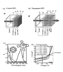
[0016] Figure 1(a) shows a schematic of a control solar cell;
[0017] Figure 1(b) shows a schematic of a full transparent solar cell
embodiment;
[0018] Figure 1(c) is a graph showing the extinction coefficient, k, of the
active layers shown in Figures 1(a) and 1(b);
[0019] Figure 1(d) is a graph showing the current-voltage (J-V) curves
for the C1A1Pc-C6o control and transparent cells shown in Figures 1(a) and
1(b);
[0020] Figure 2(a) is a graph showing the series resistance diminish
and the fill factor (FF) saturates close to the value for the control cell as
Indium Tin Oxide (ITO) thickness is increased;
[0021] Figure 2(b) is a graph showing photocurrent increase by a factor
of 3x at an optimum thickness of 120nm so that qp increases by nearly the
same amount;
[0022] Figure 3(a) is a graph showing external quantum efficiency
(EQE) as a function of wavelength for several thicknesses of ITO and control
layers;
[0023] Figure 3(b) is a graph showing transmission % as a function of
wavelength for several thicknesses of ITO and control layers;
[0024] Figure 3(c) shows the measured solar simulator spectrum
exhibiting characteristics of the Xe-lamp and NREL reported mc-Si external
quantum efficiency (EQE) for the reference-diode used to measure the solar
simulator intensity;
[0025] Figure 3(d) shows the measured and calculated reflectivity of
the distributed Bragg reflector used in this study as the transparent, NIR
mirror;
[0026] Figures 4a and 4b show solar cell arrays positioned in front of a
picture of a "rose" to highlight the transparency of the fully assembled
device;
-4-
CA 02825584 2013-07-24
WO 2012/103212
PCT/US2012/022543
[0027] Figure 4c shows a solar cell array coupled to an LCD clock;
[0028] Figures 4d and 4e show an alternate embodiment of a solar cell
array positioned in front of a picture of a "mountain" to highlight the
transparency of the fully assembled device;
[0029] Figure 4(f) is a picture of a full circuit assembly with connections
to an LCD clock.
[0030] Figure 5(a) is a graph showing external quantum efficiency
(EQE) as a function of wavelength for a SnPc device;
[0031] Figure 5(b) is a graph showing transmission % as a function of
wavelength for a SnPc device;
[0032] Figure 6(a) is a graph showing a comparison between SnPc and
ClA1Pc designs;
[0033] Figure 6(b) is a graph showing the effect of ITO cathode
thickness;
[0034] Figure 6(c) and 6(d) show the transfer matrix simulations of the
average visible transmission (AVT, left column) and short-circuit current
(right column) of the transparent OPV architecture as a function of the anode
and cathode ITO thicknesses without a NIR mirror;
[0035] Figure 6(e) and 6(f) show the transfer matrix simulations of the
average visible transmission (AVT, left column) and short-circuit current
(right column) of the transparent OPV architecture as a function of the anode
and cathode ITO thicknesses with a NIR mirror;
[0036] Figure 7 is a block diagram of a device with a mixed layer
including both a donor and an acceptor;
[0037] Figure 8 is a block diagram of a tandem device;
[0038] Figures 9(a) and 9(b) are graphs showing different bandgaps
that may be used to optimize a tandem device;
[0039] Figures 10(a) and 10(b) are graphs showing practical efficiency
limits of several of the embodiments disclosed herein;
-5-
CA 02825584 2013-07-24
WO 2012/103212
PCT/US2012/022543
[0040] Figure 11 is a diagram showing the solar flux and the photopic
response of the human eye; and
[0041] Figure 12 is a diagram showing an e-reader, smart phone and
display screen including a photovoltaic array as disclosed herein.
[0042] DETAILED DESCRIPTION OF THE INVENTION
[0043] Described herein are improved transparent solar cell designs,
e.g., transparent organic photovoltaic devices (TOPV). The term transparent
as used herein encompasses an average visible transparency of a straight
through beam of 45% or more. The term semi-transparent as used herein
encompasses an average visible transparency of a straight through beam of
approximately 10%-45%. In general, the designs include molecular active
layers with strong absorption features outside of the visible light spectrum,
e.g., in the ultra-violet (UV) and/or near-infrared (NIR) solar spectrum. The
devices may include selective high-reflectivity NIR and broadband anti-
reflection contact coatings. Devices may be formed as heterojunction solar
cells with an organic active layer, such as chloroaluminum phthalocyanine
(C1A1Pc) or SnPc as a donor and a molecular active layer such as C60 acting as
an acceptor and having peak-absorption in the UV and NIR solar spectrum.
Other suitable materials for the active layers include any suitable
phthalocyanine, porphyrin, naphthalocynanine dye, carbon nanotubes or
molecular excitonic materials with absorption peaks outside the visible
spectrum. Such devices may be formed in a tandem structure with one or
more subcells joined via a recombination zone. Such devices may be used in a
variety of applications including rigid and flexible computer display screens
used in a desktop monitor, laptop or notebook computer, tablet computer,
mobile phone, e-readers and the like. Other applications include watch
crystals, automotive and architectural glass including sunroofs and privacy
glass. The photovoltaic devices may be used for active power generation, e.g.,
-6-
CA 02825584 2013-07-24
WO 2012/103212
PCT/US2012/022543
for completely self-powered applications, and battery charging (or battery
life
extension).
[0044] Near-
infrared (NIR) as recited herein is defined as light having
wavelengths in the range from about 650 to about 850 nanometers (nm).
Ultraviolet (UV) as recited herein is defined as light having wavelengths less
than about 450 nm. The use of an active layer having absorption in the NIR
and the UV allows for the use of selective high-reflectivity near-infrared
mirror coatings to optimize device performance while also permitting high
transmission of visible light through the entire device. Visible light as
recited herein is defined as light having wavelengths to which the human eye
has a significant response, from about 450 to about 650 nm.
[0045] In one
embodiment, devices were fabricated on 150nm of
patterned Indium Tin Oxide (ITO) (15 0/sq.) pre-coated onto glass substrates.
The ITO is one component of an electrode. The ITO was solvent-cleaned and
subsequently treated in oxygen plasma for 30 seconds immediately prior to
loading into a high vacuum chamber (<1x10⁻⁶ Torr). ClA1Pc and C60 were
purified once by vacuum train sublimation prior to loading. Bathocuproine
(BCP) and molybdenum trioxide (Mo03) were used as purchased. Mo03 is
another component of an electrode. The Mo03 (20nm), ClA1Pc (15nm), C60
(30nm), BCP (7.5nm), and a 100nm thick Ag cathode were sequentially
deposited via thermal evaporation at a rate of 0.1nm/s. The top ITO cathode
for the transparent devices was rf-sputtered directly onto the organic layers
at low power (7-25W) with 10 sccm Ar flow (6 mTorr) and 0.005-
0.03nm/second. Cathodes were evaporated through a shadow mask, defining
a 1 millimeter (mm) x 1.2 mm active device area. A near-infrared distributed
Bragg reflector (DBR) utilized as the transparent NIR mirror was grown
separately on quartz via sputtering of 7 alternating layers of TiO2 and SiO2
at about 0.1nm/second with thicknesses centered around a wavelength of
800nm (200nm stop band). Broad-band antireflection (BBAR) coatings
-7-
precoated on quartz substrates (1-side) were attached to the DBRs via index
matching
fluid to reduce additional glass/air interface reflections. Transmission data
of the
assembled devices were obtained at normal incidence with a Cary Eclipse 5000
dual-
beam spectrophotometer without reference samples. Current density versus
voltage (J-
V) characteristics were measured in the dark and under simulated AM1.5G solar
illumination without solar mismatch correction (for reference, the mismatch
factor was
estimated to be ¨1.05) and external quantum efficiency (EQE) measurements were
collected utilizing an NREL calibrated Si detector. Optical interference
modeling was
carried out according to the method of L. A. A. Pettersson, L. S. Roman, and
0.
Inganas, Journal of Applied Physics 86, 487 (1999). The exciton diffusion
lengths of
ClA1Pc and Ceo were estimated from fitting the magnitudes of the photocurrent
and
EQE to be 5 3nm and 10 5nm, respectively.
[0046] Figure
1(a) shows a schematic of a control solar cell 10. The control solar
cell includes a substrate 11, an anode 12, a donor layer 13 e.g., ClA1Pc, a
molecular
active layer, e.g., Ceo, acting as an acceptor layer 14 and a cathode 15. In
this example,
the anode 15 is opaque, e.g., silver. Figure 1(b) shows a schematic of a full
transparent
solar cell 20. The device 20 generally includes a transparent substrate 21, an
anode 22,
a donor layer 23, e.g., ClA1Pc, a molecular active layer, e.g., Ceo, acting as
an acceptor
layer 24, and a cathode 25. The donor layer 23 and the acceptor layer 24 have
absorption peaks in the ultra-violet (UV) and near-infrared (N1R) spectrum. In
this
example, the substrate is quartz. It should be understood that a variety of
rigid and
flexible substrates may be used. For example, the substrate may be glass, a
rigid or
flexible polymer, e.g., a screen protector or skin, or may be combined with
other layers
such as encapsulating layers, anti-reflecting layers or the like. In this
example, the
transparent anode 22 and cathode 25 are formed of conducting oxide, e.g.
ITO/M003.
It should be
- 8 -
Date recue / Date received 2021-11-09
CA 02825584 2013-07-24
WO 2012/103212
PCT/US2012/022543
understood that the anode 22 and cathode 25 may be formed of other
materials such as tin oxides, fluorinated tin oxides, nanotubes, Poly(3,4-
ethylenedioxythiophene) (PDOT) or PED OT: P SS (Poly(3, 4-
ethylenedioxythiophene) poly(styrenesulfonate)), gallium doped zinc oxide,
aluminum doped zinc oxide and other materials having suitable transparency
and conductivity. The device 20 may also include a near-infrared DBR 26
and one or more broad-band antireflection (BBAR) coatings 27.
[0047] Figure 1(c)
is a graph showing the extinction coefficient, k, of the
active layers shown in Figures 1(a) and 1(b). Figure 1(d) is a graph showing
the current-voltage (J-V) curves for the ClA1Pc-C60 control and transparent
cells of Figures 1(a) and 1(b) for a range of thicknesses of ITO. The
absorption peak for ClA1Pc is positioned in the NIR range (-740nm). This
allows for the incorporation of a NIR reflecting mirror and simultaneous
optimization of the solar cell performance and visible-transmissivity as
diagramed in Figures 1(a) and 1(b). It should be understood that the donor
and/or acceptor layers may have one or more absorption peaks outside of the
visual spectrum. In this example, the ClA1Pc also has a second absorption
peak in the UV range. A summary of various device performances is
provided in Table 1.
-9-
CA 02825584 2013-07-24
WO 2012/103212
PCT/US2012/022543
Cathode
Cathode Jsc Voc FF Tip AVT
Thickness
Composition (mA/cm2) (V) (%) (%)
(nm)
100 Ag 4.7 0.77 0.55 2.4 0
20 ITO 1.5 0.69 0.39 0.5 67
120 ITO 3.2 0.71 0.46 1.3 65
20 ITO/NIR mir. 2.2 0.73 0.32 0.6 53
40 ITO/NIR mir. 2.5 0.71 0.49 1.1 55
80 ITO/NIR 2.9 0.71 0.46 1.2 56
120 ITO/NIR mir. 4.4 0.71 0.44 1.7 56
170 ITO/NIR min 3.2 0.69 0.48 1.3 66
Table 1
[0048] Table 1
generally includes data showing the performance of
control OPVs with an Ag cathode, transparent OPVs with ITO cathode, and
OPVs with ITO cathode and NIR mirror, at 0.8 sun illumination corrected for
solar spectrum mismatch. Short circuit current, JSC, open circuit voltage,
VOC, fill factor, FF, power conversion efficiency, qp, and the average visible
transmission, AVT, are indicated. The control device with a thick Ag cathode
exhibits a power conversion efficiency (77p) of 1.9+0.2%, open circuit voltage
(Voc) = 0.80 0.02V, short-circuit current density (Jsc) = 4.7 0.3mA/cm2, and
fill-factor (FF) = 0.55+0.03, which is comparable to previous reports.
[0049] When the Ag
cathode of the control cell is replaced with ITO, the
short-circuit current Jsc drops significantly to 1.5 0.1mA/cm2, the FF drops
to 0.35+0.02, and the open-circuit voltage Voc decreases slightly to 0.7+0.02V
leading to 77p -= 0.4+0.1%. The FF decreases due to an increase in series
resistance from the thin ITO that is observable in the J-V curve under
forward bias in Figure 1(c). Figure 2(a) is a graph showing the series
resistance diminish and the FF saturate close to the value for the control
cell
-10-
CA 02825584 2013-07-24
WO 2012/103212
PCT/US2012/022543
as ITO thickness is increased. In Figures 2(a) and 2(b), the solid lines are
from actual simulations, the dashed lines are simply guides to the eye. The
slight drop in Voc, independent of ITO thickness, is likely due to a slight
reduction in the cathode-anode work function offset. Nonetheless it is
remarkable that when utilizing ITO as both anode and cathode there is
enough deposition anisotropy in the work function to support this large Voc
and is likely assisted by the large work function Mo03 layer.
[0050] The Jsc
decreases as the cathode is switched from Ag to ITO due
to reduced cathode reflections that reduce the total absorption across the
spectrum in the active layers. Figure 2(b) is a graph showing photocurrent
increase by a factor of 3x at an optimum thickness of 120nm so that rip
increases by nearly the same amount. Fitting this data with the optical
interference model shows that this behavior stems from interference of the
backside ITO cathode reflection. Figure 3(a) is a graph showing EQE as a
function of wavelength for several thicknesses of ITO and control layers with
and without NIR reflecting mirrors. The approximate visible photopic range
is highlighted by vertical dashed lines. Figure 3(b) is a graph showing
transmission % as a function of wavelength for several thicknesses of ITO
and control layers. Comparing EQE and transmission of the ITO-only
devices, the absorption for the thinnest and optimized thicknesses appears
equivalent. Inspection of the simulations shows, however, that the NIR field
distribution is shifted from within the ITO anode to the C1A1Pc active layer
as the ITO cathode thickness increases, so that the total transmission
appears the same even though the active layer absorption changes
substantially. This highlights an important aspect of transparent OPV
architectures; despite the seemingly simple optical configuration,
interference
management is still crucial to device optimization, particularly for NIR
absorbing cells and for materials with low exciton diffusion lengths.
-11-
[0051] Despite the significant impact on the photocurrent, the average
visible
transmissivity (AVT) shows little variation with ITO thickness (see e.g.,
Figure 2(a)).
The optical model predicts a slight decrease in AVT with ITO thicknesses that
is not
observed experimentally possibly due to model parameter uncertainties or
varying
optical constants during thicker ITO growths. Optimized cells without the NIR
mirror
show min (max) transmission values of 50% (74%) at 450nm (540nm) and an AVT of
65% (standard deviation of 7%). These transmission values decrease slightly
with the
incorporation of the NIR reflector to min (max) transmission values of 47%
(68%) at
450nm (560nm) and an AVT of 56% (standard deviation of 5%), where this
reduction
results from increased off-resonance visible reflections of the mirror. It is
possible to
remove the off-resonance reflection oscillations in the visible spectra by
designing
more complex hot-mirror architectures to improve the AVT closer to that of the
cell
without the NIR mirror, but this typically requires a greater number layers.
Hot mirror
architectures are described in A. Thelen, Thin Films for Optical Systems 1782,
2
(1993). High reflectivity of 99% between 695-910 nm also makes these devices
useful
for simultaneous NIR rejection in architectural cooling. Additionally, the use
of the
BBAR coatings next to the DBR (outcoupling) and below the substrates
(incoupling),
results in a concomitant increase in the quantum efficiency by ¨2-3% and the
AVT by
¨4-6%.
[0052] Figure 3(c) shows the measured solar simulator spectrum (left axis)
exhibiting characteristics of the Xe-lamp and NREL reported mc-Si external
quantum
efficiency (EQE) for the reference- diode used to measure the solar simulator
intensity
(right-axis). Because the responsivity of the reference diode extends
significantly
beyond the response of the OPV cell, the extra NIR light from the solar
simulator
(compared to the AM1.5G spectrum) results in solar mismatch factors less than
1.
Figure 3(d) shows the
- 12 -
Date recue / Date received 2021-11-09
CA 02825584 2013-07-24
WO 2012/103212
PCT/US2012/022543
measured (left axis, circles) and calculated (left axis, solid line)
reflectivity of
the distributed Bragg reflector used in this study as the transparent, NIR
mirror. Also shown is the transmission spectrum (right-axis) of the broad-
band antireflection (BBAR) coatings.
[0053] To
highlight the transparency of the fully assembled device,
Figures 4a and 4b show solar cell arrays in front of a picture of a "rose".
Both
picture-detail and color-clarity are minimally disrupted so that details of
the
device array pattern are even difficult to discern. In this example the array
has a common cathode 25a and a plurality of anodes 22a. The device also
includes an active area 30 which includes the donor layer(s), acceptor
layer(s)
and reflective mirrors. In this particular example, an array of 10 individual
OPV devices is formed on the substrate 21a. Figure 4(c) shows the array
wired to power an LCD clock. Figures 4(d) and 4(e) show an alternate
embodiment of a solar cell array positioned in front of a picture of a
µ`mountain" to highlight the transparency of the fully assembled device.
[0054] Figure 4(f)
is a picture of a full circuit assembly (left). Electrical
connections are made to the ITO contacts of the OPV device (array) via
carbon-tape. The LCD clock is connected to circuitry (right) that limits the
voltage and passes excess current to a small LED such that the clock works
under a wide range of OPV illumination conditions. The LCD clock requires
approximately 1.5V and 10 A and can be run by the solar cell for intensities
> 0.05 suns (note that under the ambient lighting < 0.01 sun, the clock is
off).
[0055] Optimizing
the transparent OPV structure with just the cathode
thickness, power conversion efficiency of 1.0+0.1% is obtained, with a
simultaneous average transmission of 66 3%. Incorporation of the NIR
reflector and BBAR coatings with the optimized ITO thickness (see Figure
2(a)) improves the power conversion efficiency to 1.4+0.1% with an average
transmission of 56 2%. With the NIR mirror, the increase in power
conversion efficiency stems from additional NIR photocurrent in the C1A1Pc
-13-
CA 02825584 2013-07-24
WO 2012/103212
PCT/US2012/022543
layer where the EQE shows a near doubling of the peak ClA1Pc EQE from
10% to 18% (see Figure 3(a)). The optimized power efficiency is nearly triple
that of an existing visible-absorbing, semi-transparent, copper
phthalocyanine planar device while also exhibiting 30% more average
transmission, but is slightly less efficient (0.75x) than semi-transparent
bulk-
heterojunction structures that gain efficiency from active layer absorption in
the visible and subsequently have nearly half the transmission.
[0056] Switching
from planar to bulk-heterojunctions in these
structures, efficiencies of 2-3% may be possible for this material set with
nearly identical visible transmission, and is currently under investigation.
Tandem stacking of subcells with active layer absorption deeper into the
infrared could also enhance these efficiencies; combined with more
sophisticated NIR mirrors, efficiencies beyond several percent and average
visible transmission >70% are possible.
[0057] In another
embodiment, SnPc, e.g., SnPc-C60, may be used to
construct transparent solar cells. Solar cell designs based on SnPc may
achieve >2% efficient solar cell with >70% transmission of visible light (-70%
average transmission across visible spectrum). The following layers were
used in this example: ITO / SnPc(10nm) / C60(30nm) / BCP(10nm) /
ITO(10nm) / DBR. In this example, the ITO was sputtered directly. The
distributed Bragg reflectors (DBR) were applied with index matching fluid
(IMF). Figure 5(a) is a graph showing the EQE as a function of wavelength
for the SnPc device. Figure 5(b) is a graph showing transmissivity as a
function of wavelength for the full TOPV SnPc device. A summary of various
device performances is provided in Table 2:
-14-
CA 02825584 2013-07-24
WO 2012/103212
PCT/US2012/022543
Cathode Jsc Voc FF n (%)
Ag 6.15 0.40 0.55 1.3
ITO 1.54 0.33 0.48 0.2
ITO-DBR 2.25 0.34 0.44 0.3
Table 2
[0058] The device
may include a NIR mirror (transparent to visible
light) composed of either metal/oxide (e.g. Ti02/Ag/Ti02) or dielectric stacks
(DBRs e.g. consisting of SiO2/TiO2). Anti-
reflection coatings may be
composed of single or multilayer dielectric materials. As noted above, the
molecular active layer may also be composed of any suitable phthalocyanine,
porphyrin, naphthalocyanine dye, carbon nanotube, or molecular excitonic
materials with absorption peaks outside of the visible spectrum.
[0059] Figure 6(a)
is a graph showing a comparison between SnPc and
ClA1Pc reference (opaque) designs. A summary
of various device
performances is provided in Table 3:
Donor Thick Jsc Voc FE n (%)
SnPc 100 6.15 0.40 0.50 1.2
CIAIPc 200 4.70 0.77 0.55 2.0
Table 3
[0060] Figure 6(b)
is a graph showing the electric field and the effect of
ITO cathode thickness. Calculated optical field, 1E12, of the transparent
OVP as a function of position at a fixed wavelength close to the peak
absorption of the ClA1Pc active layer (-740nm) for an ITO cathode thickness
of 20nm (black line) and 120nm (red line). Note the enhancement of the field
within the ClA1Pc layer for the optimized ITO thickness, where the
absorption is proportional to IE I 2 integrated over position. In general,
there
is a strong dependence on ITO thickness.
-15-
CA 02825584 2013-07-24
WO 2012/103212
PCT/US2012/022543
[0061] Figures
6(c) and 6(d) show the transfer matrix simulations of the
average visible transmission (AVT, left column) and short-circuit current
(right column) of the transparent OPV architecture as a function of the anode
and cathode ITO thicknesses without a NIR mirror. Figures 6(e) and 6(0
show the transfer matrix simulations of the average visible transmission
(AVT, left column) and short-circuit current (right column) of the transparent
OPV architecture as a function of the anode and cathode ITO thicknesses
with a NIR mirror. The vertical dashed line indicates the thickness of the
ITO anode utilized in this study. The active
layer structure was
Anode/Mo03(20nm) / ClA1Pc(15nm) / C60(30nm) / BCP(7.5nm) / Cathode
where the exciton diffusion lengths of ClA1Pc and C60 were estimated from
fitting the magnitudes of the photocurrent and EQE of the control cell to be
8 4nm and 15 6nm, respectively.
[0062] The
structure shown in Figure 1(b) includes discrete layers for
the donor, e.g., ClA1Pc or SnPc, and the acceptor, e.g., C60. It should be
understood that the donor and acceptor may be combined in a single or mixed
layer as shown generally in Figure 7. In this embodiment the device 40 may
have a mixed layer 46 including both a donor and an acceptor. The mixed
layer generally has a thickness dmixed as shown. The device 40 may optionally
include a discrete donor layer 48 and/or acceptor layer 46. The donor layer
48, if present, has a thickness dnonor as shown. The acceptor 46 layer, if
present, has a thickness dAcceptor as shown. It should be understood that
Figure 7 is simplified for matters of clarity and may include additional
layers
that are not shown. In this example, the device 40 also includes a
transparent cathode 42 and a transparent anode 50. The thicknesses of each
layer may be selected as generally outlined above. It should be understood
that such a structure may also include other layers including anti-reflective
layers and mirror layers as disclosed in the various embodiments herein.
[0063] An optimization process may generally be performed as follows:
-16-
CA 02825584 2013-07-24
WO 2012/103212
PCT/US2012/022543
[0064] i) Optimize for dDonor, dAcceptor (total);
[0065] ii) Fix dDonor, dAcceptor (total);
[0066] iii) Vary dmixed;
[0067] iv) dDonor¨ dDonor (total) ¨ (dmixed/2);
[0068] V) dAcceptor = dAcceptor (total) ¨ (dmixed/2); and
[0069] vi) Optimize for ratio (dDonor:dAcceptor).
[0070] For devices having a mixed layer only, optimization may include
an adjustment of the thickness of the mixed layer (step iii) and an
adjustment of the ratio dnorior:dAccemor (step vi).
[0071] Figure 8 is a block diagram of a tandem device 60. The device
60 generally includes at least a first and second cell 66, 68. Each cell may
have the structure generally disclosed above. Each of the first and second
cells 66, 68 function has transparent subcells. Each may have a varying NIR
spectral responsivity. Each of the first and second cells may have absorption
peaks at wavelengths outside of the visible light spectrum. A recombination
zone 72a is disposed between the first and second cells 66, 68. The
recombination zone may be composed of a variety of compounds including,
e.g., ITO(0.5-10nm), or BCP/Ag(0.1-2nm)/ MoOx. Additional recombination
zones are disposed between subsequent pairs of subcells as generally shown
by reference number 72b. It should be understood that Figure 8 is simplified
for matters of clarity and may include additional layers that are not shown.
In this example, the device 60 also includes a cathode 62 and an anode 70.
The device may optionally include a transparent NIR mirror 62. Figures 9(a)
and 9(b) are graphs showing different bandgaps associated with materials
that may be used to optimize a device, e.g., US J. Aggregate (Figure 9(a)) and
carbon nanotubes (Figure 9(b)).
[0072] It should be understood that multiple bandgaps may be selected
for successive layers stacked in a tandem device in order to yield a device
with the desired efficiency. In such devices, overall transparency is improved
-17-
CA 02825584 2013-07-24
WO 2012/103212
PCT/US2012/022543
over devices that are independently fabricated and post integrated or
macroscopically combined. This is possible because such a device benefits
from a closely matched index of refraction at each interface between
successive layers. The stacked structure may be transparent or semi-
transparent.
[0073] Figures
10(a) and 10(b) are graphs showing practical efficiency
limits of several of the embodiments disclosed herein. Figure 11 is a diagram
showing solar flux and the photopic response of the human eye. In general,
the photopic response of the human eye peaks in the green spectrum 530-
500nm and tapers off below 450nm and above 650nm.
[0074] Figure 12
is a diagram showing an e-reader 80, smart phone 82
and display screen 84 including photovoltaic arrays 86, 88 and 90 disposed on
their respective display screens. It should be understood that a variety of
devices may incorporate the photovoltaic devices disclosed herein and/or
arrays of such devices. Other applications include watch crystals, automotive
and architectural glass including sunroofs and privacy glass. The
photovoltaic devices may be used for active power generation, e.g., for
completely self-powered applications and battery charging (or battery life
extension).
[0075] In
conclusion, near-infrared absorbing, transparent planar
organic solar cells with a maximum power of 1.4 0.1% and average visible
transmission of exceeding 55 2% have been demonstrated. This average
visible transmission is sufficiently transparent for incorporation on
architectural glass. The excitonic character of organic semiconductors is
advantageously exploited to produce unique photovoltaic architectures not
easily accessible via inorganic semiconductors. By positioning the active
layer absorption selectively in the NIR, it is possible to optimize the
architecture using a NIR reflector composed of a DBR mirror centered at
800nm that results in a transparent solar cell efficiency approaching that of
-18-
CA 02825584 2013-07-24
WO 2012/103212
PCT/US2012/022543
the non-transparent control cell. Ultimately these devices provide a guide for
achieving high efficiency and high transparency solar cells that can be
utilized in windows to generate power, reduce cooling costs, and scavenge
energy in a variety of applications.
-19-