Note: Descriptions are shown in the official language in which they were submitted.
V
CA 02825727 2013-07-25
DocketNo.PTRA-13114-PCT
1
DESCRIPTION
MICROARRAY ANALYSIS METHOD AND MICROARRAY READING DEVICE
Field
[0001] The present invention relates to a microarray
analysis method and a microarray reading device.
Background
[0002] A technology called microarray has been advanced
to be developed and used in biological, medical, and
pharmaceutical fields since 1990. The microarray is
obtained by immobilizing several tens to several tens of
thousands of probes onto a substrate made of glass, plastic,
or the like and applying a sample (target) labeled with
fluorescent molecules or the like to the substrate so as to
L.,:e..i.L:tion between the probe aria the la-pi
with fluorescence or the like. The microarrays have a
characteristic that makes it possible to perform
comprehensive measurement at one time and are expected to
be essential to personalized medicine in the future.
[0003] The probes to be immobilized onto the substrate
include the following types and the microarrays are named
based on the types of the probes. That is to say, well-
known have been a DNA microarray (DNA chip) obtained by
immobilizing DNAs as the probes onto the substrate, a
protein microarray obtained by immobilizing proteins as the
probes onto the substrate, a tissue microarray obtained by
immobilizing a number of small specimens as the probes onto
the substrate, a compound microarray obtained by
immobilizing a number of low-molecular compounds as the
probes onto the substrate, and the like.
[0004] Among them, the DNA microarray (hereinafter,
referred to as DNA chip) has been put into practical use at
the most advanced level. Studies have been performed
actively on analyses of genes relating to diseases, and
CA 02825727 2013-07-25
DocketNo.PTRA-13114-PCT
2
examination and diagnosis by using the genes and some of
them have been put into practical use.
[0005] Described is the DNA chip as one mode of the
microarray in detail below.
[0006] The DNA chip is obtained by spotting
(immobilizing) DNAs onto the substrate made of glass, resin,
or the like in a grid form. The DNAs (probe DNAs) as the
probes that can react with the DNA sample to be labeled
specifically are spotted on the DNA chip. Optically
detectable luminescent or fluorescent mark is added to an
unknown DNA sample to be analyzed. The unknown DNA sample
to be analyzed is made to flow onto the DNA chip. With
this, the DNA sample bonds to the spotted DNA to form a
aoubie strand if the unknown DNA sample and the spoLted DNA
have a complementary relation. Then, all the DNA samples
that have not bonded to the probe DNAs are washed out, the
DNA samples to be determined that remain on the DNA chip
are made luminescent, and the DNA chip is read by a reading
device (scanner). This makes it possible to observe the
state of the double-stranded DNA as an image. That is to
say, distribution of luminescent marks on the DNA chip is
analyzed so as to analyze presence of the gene to be
obtained, expression of a certain gene, or the degree of
expression of the gene. In this manner, an already-known
probe DNA set is configured on the DNA chip and the probe
DNAs are mounted on a number of types of DNA chips so as to
detect genetic alteration, an expression amount of the gene,
and the like.
[0007] Hereinafter, FIG. 1 illustrates a series of
processing processes of DNA chip analysis in detail.
[0008] In a preprocessing process as illustrated in FIG.
1, unknown DNA contained in a DNA sample extracted from a
specimen is amplified and a fluorescent mark is added to
CA 02825727 2013-07-25
=
DocketNo.PTRA-13114-PCT
3
the DNAs.
[0009] In the subsequent hybridization process, the DNA
sample added with the fluorescent mark (for example, Cy3,
Cy5, or the like) are made to drop onto the substrate of
the DNA chip on which a number of types of probe DNA have
been mounted. The DNA sample bonds to the spotted DNA to
form a double strand if the DNA sample and the spotted DNA
have a complementary relation.
[0010] Next, in the washing process, the hybridized DNA
chip is washed with predetermined washer fluid. With this,
all the DNA samples that have not bonded to the probe DNAs
arranged in the grid form are washed out.
[0011] Subsequently, the washed DNA chip is scanned. In
the scanning process, the DNA chip is irradiated with a
laser beam having a predetermined wavelength suitable for
exciting the fluorescent mark (for example, Cy3, Cy5, or
the like) so as to be scanned in the reading device. With
this, amounts of luminescence of the respective spotted
DNAs (genes) are measured and fluorescence image data on
which analysis processing is to be performed based on the
amounts of luminescence is acquired.
[0012] In the analysis process, a fluorescence intensity
of each spot is calculated by using a template for the
obtained fluorescence image data and various types of
analyses are executed.
[0013] FIG. 2 illustrates an example of a DNA chip 1 to
be used for DNA chip analysis. The DNA chip 1 as
illustrated in FIG. 2 includes blocks on a substrate 2. On
each of the blocks, a predetermined number of probe DNAs
corresponding to individual genes are arrayed in rows and
columns in a matrix form (hereinafter, the probe DNA
arranged on the block is referred to as a "spot" 3). It is
to be noted that the spots 3 arranged on the substrate 2
CA 02825727 2013-10-15
55226-7
4
correspond to genes of which base sequences have been already
mapped and that are different from one another and arrangement
positions of the spots 3 on the substrate 2 have been defined
previously.
[0014] FIG. 3 illustrates an example of the template to be
applied to the fluorescence image data of the DNA chip. As
illustrated in FIG. 3, the template is divided into a plurality
of blocks of 1 to 32, for example. Detection areas
(corresponding to individual spots of the DNA chip) that are
arranged in a matrix form of m rows x n columns (22 x.22 in
FIG. 3) are provided on each block.
[0015] In the above-mentioned analysis process, the
detection areas on the template provided by an analysis tool
are assigned to the individual spots in the fluorescence image
data read from a DNA chip (alignment) so as to calculate.
fluorescence intensities of the respective spots in the
corresponding detection areas. In this case, the alignment
processing needs to be executed accurately such that the
individual detection areas of the template are set correctly to
the individual spots on the image in order to execute accurate
analysis.
[0016] The alignment method includes a pattern matching
method and a projection method in which alignment is made on a
block basis. As described in Patent Literature 1, alignment
tries to be performed accurately by using a chip spotted with a
fluorescent substance called positive control or a house-
keeping gene contained in any specimens.
CA 02825727 2013-10-15
55226-7
Citation List
Patent Literature
[0017] Patent Literaturel: Japanese Laid-open Patent
Publication No. 2005-172840
=
5 Summary
[0018] With any of the typical pattern matching method and
projection method in which alignment is made on a block basis,
alignment cannot be performed accurately unless an amount of
hybridized sample DNAs is large and 1/4 to approximately half
spots that emit fluorescence having a sufficient intensity are
present. When the sample extracted from the specimen contains
a small amount of DNAs, alignment cannot be performed
accurately in some cases. On the other hand, the method by
arranging the fluorescent substance called positive control has
an advantage that alignment can be performed even if spots =that
emit fluorescence having a sufficient intensity are less. The
method, however, has problems in that the number of DNAs
capable of being arranged is reduced and the cost is increased
at the time of the chip manufacturing, for example.
Furthermore, when the fluorescent substance is used as the
positive control, the fluorescent substance liberates during
the hybridization to contaminate the periphery of the ,positive
control. This arises a risk that data cannot be obtained.
Moreover, when the DNA probes corresponding to the house-
keeping genes are arranged, if the sample extracted from the
specimen contains a small amount of DNAs, fluorescence from the
positive control is weak and it becomes difficult to perform
alignment, as a result.
CA 02825727 2013-10-15
=
55226-7
6
[0019] Some embodiments of the present invention may solve
the above-mentioned problems and some embodiments of the
present invention may provide an analysis method and an
analysis device that makes it possible to perform alignment
processing appropriately in the analysis of a DNA chip on which
no positive control is arranged or in the analysis of a chip in
which a sample contains a small amount of DNAs.
[0020] Some embodiments of the present invention have a
characteristic of any one of the following configurations.
(1) A microarray analysis method in which a microarray obtained
by arranging probes on a substrate surface having an irregular
shape is irradiated with excitation light and fluorescence
amounts of the probes excited by the excitation light are
obtained as numerical data, the microarray analysis method
including: a step (a) of measuring the fluorescence amounts of
the probes to acquire fluorescence image data; a step (b) of
receiving reflected light and/or scattered light from the
substrate surface to acquire the irregular shape of the
substrate surface of the microarray as alignment image data
based on light receiving intensities of the light; and a step
(c) of determining positions of the probes on the fluoreScence
image data based on the alignment image data.
(2) The microarray analysis method according to the above
described (1), wherein the reflected light and/or the scattered
light from the substrate surface is light from a light source
emitting the excitation light that has been reflected and/or
scattered by the microarray.
CA 02825727 2013-10-15
55226-7
6a
(3) The microarray analysis method according to the above
described (1) or (2), wherein the step (c) includes:- d. step
(cl) of detecting equal to or more than three reference
points A of the microarray based on a difference in the light
receiving intensities on the alignment image data; and a
step (c2) of correcting strain of the fluorescence image data
based on the detected reference points A.
(4) The microarray analysis method according to the above-
described (3), wherein the step (cl) includes: a step (cl) of
calculating a contour reference point a as points on a contour
of the substrate on each of at least eight
=
=
=
=
CA 02825727 2013-07-25
DocketNo.PTRA-13114-PCT
7
predetermined observation regions; a step (c2) of pairing
at least two predetermined observation regions that are not
overlapped as sets to obtain approximate straight lines
with respect to a plurality of contour reference points a
for the respective sets; and a step (c3) of calculating
intersecting points of the approximate straight lines
obtained for the respective sets to set the intersecting
points as the reference points A.
(5) The microarray analysis method according to the above-
described (3) or (4), wherein at the step (c2), array
angles Ox and Oy of spots on which the probes are arranged
are obtained from the reference points A and shear
deformation strain of the fluorescence image data is
corrected based on the array angles Ox and Oy of the spots
and the following equations.
[0021]
(X\ ( 1 0\(x\
(1)
- tan Oxy 1 y
\ ) i\
[0022]
Oxy. = Ox- gy. (2)
[0023] (6) The microarray analysis method according to
any one of the above-described (3) to (5), wherein at the
step (cl), four reference points A are detected, and when a
quadrangular shape formed by connecting the four reference
points A with straight lines is not a parallelogram, the
quadrangular shape is made to approximate to a
parallelogram and the vertices of the parallelogram are set
as the reference points A again.
(7) The microarray analysis method according to any one of
the above-described (1) to (6), wherein the microarray is a
DNA microarray.
(8) A microarray reading device including: a laser light
81772907
8
source that irradiates a microarray obtained by arranging
probes on a substrate surface having an irregular shape with
excitation light; an objective lens that makes a light flux of
the excitation light reflected by the substrate surface and
fluorescence from the probes be parallel light; an optical
filter that cuts the excitation light reflected by the
substrate surface and through which fluorescence from the
probes penetrate; and an imaging lens and a detector that
receive the fluorescence penetrated through the optical filter
and acquire fluorescence image data, wherein the imaging lens
and the detector receive light reflected and/or scattered by
the substrate surface so as to acquire alignment image data on
which the irregular shape of the substrate surface of the
microarray is expressed, and the microarray reading device
further comprises an arithmetic processing unit that detects
positions of the probes on the fluorescence image data based on
the alignment image data.
(9) The microarray reading device according to the above-
described (8), wherein a pinhole restricting a subject depth is
provided between the imaging lens and the detector.
[0024] According to some embodiments of the present
invention, alignment processing may be performed appropriately
even in the analysis of a DNA chip on which no positive control
is arranged or in the analysis of a chip in which a sample
contains a small amount of DNAs, thereby allowing analyses.
[0024a] According to one embodiment of the present invention,
there is provided a microarray analysis method in which a
microarray obtained by arranging probes on a substrate surface
having an irregular shape is irradiated with excitation light
CA 2825727 2017-11-10
81772907
9
and fluorescence amounts of the probes excited by the
excitation light are obtained as numerical data, the microarray
analysis method comprising: a step (a) for measuring the
fluorescence amounts of the probes to acquire fluorescence
image data; a step (b) for receiving reflected light and/or
scattered light from the substrate surface to acquire the
irregular shape of the substrate surface of the microarray as
alignment image data based on light receiving intensities of
the light; and a step (c) for determining positions of the
probes on the fluorescence image data based on the alignment
image data, wherein the step (c) comprises: a step (c1) of
detecting equal to or more than three reference points A of the
microarray based on a difference in the light receiving
intensities on the alignment image data, wherein the step (cl)
comprises: a step of calculating a contour reference point a as
points on a contour of the substrate on each of at least eight
predetermined observation regions; a step of pairing at least
two predetermined observation regions that are not overlapped
as sets to obtain approximate straight lines with respect to a
plurality of contour reference points A for the respective
sets; and a step of calculating intersecting points of the
approximate straight lines obtained for the respective sets to
set the intersecting points as the reference points A; and a
step (c2) for correcting shear deformation strain of the
fluorescence image data based on the detected reference points
A and to provide a corrected fluorescence image.
[0024b] According to another embodiment of the present
invention, there is provided a microarray analysis method in
which a microarray obtained by arranging probes on a substrate
surface having an irregular shape is irradiated with excitation
CA 2825727 2018-07-30
81772907
9a
light and fluorescence amounts of the probes excited by the
excitation light are obtained as numerical data, the microarray
analysis method comprising: a step (a) for measuring the
fluorescence amounts of the probes to acquire fluorescence
image data; a step (b) for receiving reflected light and/or
scattered light from the substrate surface to acquire the
irregular shape of the substrate surface of the microarray as
alignment image data based on light receiving intensities of
the light; and a step (c) for determining positions of the
probes on the fluorescence image data based on the alignment
image data, wherein the step (c) comprises: a step (c1) of
detecting equal to or more than three reference points A of the
microarray based on a difference in the light receiving
intensities on the alignment image data; and a step (c2) for
correcting shear deformation strain of the fluorescence image
data based on the detected reference points A and to provide a
corrected fluorescence image, wherein at the step (c2), array
angles Ox and Oy of spots on which the probes are arranged are
obtained from the reference points A and shear deformation
strain of the fluorescence image data is corrected based on the
array angles Ox and Oy of the spots and the following
equations:
1 0\(x\
=
tan Oxy lAy j
Oxy = Ox -0y
wherein (x,y) corresponds to coordinates before correction and
(X,Y) corresponds to coordinates after correction, array angle
Ox is an inclination angle of a line connecting most adjacent
spots linearly with respect to an x-axis of the substrate
surface, array angle Oy is the inclination angle of a line
CA 2825727 2018-07-30
81772907
9b
connection most adjacent spots linearly with respect to a y-
axis of the substrate surface.
[0024c] According to still another aspect of the present
invention, there is provided a microarray analysis method in
which a microarray obtained by arranging probes on a substrate
surface having an irregular shape is irradiated with excitation
light and fluorescence amounts of the probes excited by the
excitation light are obtained as numerical data, the microarray
analysis method comprising: a step (a) for measuring the
fluorescence amounts of the probes to acquire fluorescence
image data; a step (b) for receiving reflected light and/or
scattered light from the substrate surface to acquire the
irregular shape of the substrate surface of the microarray as
alignment image data based on light receiving intensities of
the light; and a step (c) for determining positions of the
probes on the fluorescence image data based on the alignment
image data, wherein the step (c) comprises: a step (cl) of
detecting at least four reference points A of the microarray
based on a difference in the light receiving intensities on the
alignment image data, and when a quadrangular shape formed by
connecting the at least four reference points A with straight
lines is not a parallelogram, the quadrangular shape is made to
approximate to a parallelogram and the vertices of the
parallelogram are set as the reference points A again; and a
step (c2) for correcting shear deformation strain of the
fluorescence image data based on the detected reference points
A and to provide a corrected fluorescence image.
[0024d] According to yet another aspect of the present
invention, there is provided a microarray reading device
CA 2825727 2018-07-30
81772907
9c
comprising: a laser light source that irradiates a microarray
obtained by arranging probes on a substrate surface having an
irregular shape with excitation light; an objective lens that
makes a light flux of the excitation light reflected by the
substrate surface and fluorescence from the probes be parallel
light; an optical filter that cuts the excitation light
reflected by the substrate surface and through which
fluorescence from the probes penetrate; and an imaging lens and
a detector that receive the fluorescence penetrated through the
optical filter and acquire fluorescence image data, the imaging
lens and the detector receiving light reflected and/or
scattered by the substrate surface so as to acquire alignment
image data on which the irregular shape of the substrate
surface of the microarray is expressed; and an arithmetic
processing unit that detects positions of the probes on the
fluorescence image data based on the alignment image data,
wherein the arithmetic processing unit is configured to detect
three or more reference points A of the microarray based on a
difference in the light receiving intensities on the alignment
image data by calculating a contour reference point a as points
on a contour of the substrate on each of at least eight
predetermined observation regions, pairing at least two
predetermined observation regions that are not overlapped as sets
to obtain approximate straight lines with respect to a plurality
of contour reference points A for the respective sets, and
calculating intersecting points of the approximate straight lines
obtained for the respective sets to set the intersecting points
as the reference points A, and correcting shear deformation
strain of the fluorescence image data based on the detected
reference points A and provides a corrected fluorescence image.
CA 2825727 2018-07-30
81772907
9d
[0024e] According to a further aspect of the present
invention, there is provided a microarray reading device
comprising: a laser light source that irradiates a microarray
obtained by arranging probes on a substrate surface having an
irregular shape with excitation light; an objective lens that
makes a light flux of the excitation light reflected by the
substrate surface and fluorescence from the probes be parallel
light; an optical filter that cuts the excitation light
reflected by the substrate surface and through which
fluorescence from the probes penetrate; an imaging lens and a
detector that receive the fluorescence penetrated through the
optical filter and acquire fluorescence image data, the imaging
lens and the detector receiving light reflected and/or
scattered by the substrate surface so as to acquire alignment
image data on which the irregular shape of the substrate
surface of the microarray is expressed; and an arithmetic
processing unit that detects positions of the probes on the
fluorescence image data based on the alignment image data,
wherein the arithmetic processing unit is configured to detect
three or more reference points A of the microarray based on a
difference in the light receiving intensities on the alignment
image data and to correct shear deformation strain of the
fluorescence image data based on the detected reference points
A and to provide a corrected fluorescence image, wherein array
angles Ox and Oy of spots on which the probes are arranged are
obtained from the reference points A and shear deformation
strain of the fluorescence image data is corrected based on the
array angles Ox and Oy of the spots and the following
equations:
CA 2825727 2018-07-30
81772907
9e
1 0\(x
-tanOxy 1,ky1
Oxy = Ox - By
wherein (x,y) corresponds to coordinates before correction and
(X,Y) corresponds to coordinates after correction, array angle
Ox is an inclination angle of a line connecting most adjacent
spots linearly with respect to an x-axis of the substrate
surface, array angle By is the inclination angle of a line
connection most adjacent spots linearly with respect to a y-
axis of the substrate surface.
[0024f] According to yet a further aspect of the present
invention, there is provided a microarray reading device
comprising: a laser light source that irradiates a microarray
obtained by arranging probes on a substrate surface having an
irregular shape with excitation light; an objective lens that
makes a light flux of the excitation light reflected by the
substrate surface and fluorescence from the probes be parallel
light; an optical filter that cuts the excitation light
reflected by the substrate surface and through which
fluorescence from the probes penetrate; an imaging lens and a
detector that receive the fluorescence penetrated through the
optical filter and acquire fluorescence image data, the imaging
lens and the detector receiving light reflected and/or
scattered by the substrate surface so as to acquire alignment
image data on which the irregular shape of the substrate
surface of the microarray is expressed; and an arithmetic
processing unit that detects positions of the probes on the
fluorescence image data based on the alignment image data,
wherein the arithmetic processing unit is configured to detect
four reference points A of the microarray based on a difference
CA 2825727 2018-07-30
81772907
9f
in the light receiving intensities on the alignment image data
and form a quadrangular shape that is not a parallelogram by
connecting the four reference points A with straight lines and
making the quadrangular shape approximate a parallelogram and
setting the vertices of the parallelogram as the reference points
A, and to correct shear deformation strain of the fluorescence
image data based on the reference points A of the parallelogram
and to provide a corrected fluorescence image.
Brief Description of Drawings
[0025] FIG. I is a schematic diagram illustrating a series
of processes in DNA chip analysis.
FIG. 2 is a schematic view illustrating an example of
a DNA chip to be used in the DNA chip analysis.
FIG. 3 is a plan view illustrating an example of a
template to be applied to fluorescence image data of the DNA
chip in the DNA chip analysis.
FIG. 4 is a schematic plan view illustrating a DNA
chip analysis device as one embodiment of the invention.
FIG. 5 is a schematic plan view illustrating an
embodiment of an optical system in a DNA chip reading device.
FIG. 6 is a plan view illustrating an example of
fluorescence image data on which strain is generated and spot
array is not perpendicular although a DNA chip on which the row
direction and the columnar direction of the spot array are
orthogonal to each other perpendicularly has been scanned.
CA 2825727 2018-07-30
81772907
9g
FIG. 7 is a view illustrating an example of an
alignment image obtained by the DNA chip reading device.
FIG. 8 is a block diagram illustrating one embodiment
of a DNA chip analysis method.
FIG. 9 is a view illustrating coordinates of four
corners on the alignment image obtained by the DNA chip reading
device.
FIG. 10 is a view illustrating processing at Step 4
and Step 5 in FIG. 8.
FIG. 11 is a view illustrating examples of the
alignment image data (a) and fluorescence image data (b) and
(c) subjected to analysis in the invention.
FIG. 12 is a view illustrating an example of a method
of detecting reference points.
FIG. 13 is a view when the DNA chip is rotated on the
alignment image data.
FIG. 14 is a view illustrating a method of
approximating a trapezoidal shape to a parallelogram.
Description of Embodiments
[0026] A microarray analysis device according to the
CA 2825727 2018-07-30
CA 02825727 2013-07-25
DocketNo.PTRA-13114-PCT
invention is a device that analyzes a DNA microarray (DNA
chip) obtained by immobilizing DNAs as probes onto a
substrate, a protein microarray obtained by immobilizing
proteins as the probes onto the substrate, a tissue
microarray obtained by immobilizing a number of small
specimens onto the substrate, a compound microarray
obtained by immobilizing a number of low-molecular
compounds onto the substrate, and the like. The microarray
analysis device performs alignment of fluorescence image
10 data to be obtained by using an irregular shape of the
substrate surface of the microarray. In the analysis
device, the microarray on which probes are arranged on the
substrate surface having the irregular shape is irradiated
w.1,h excitation light so as to obtain fluorescencc an.ounts
from the respective probes excited with the excitation
light as pieces of numerical data. In this case, the
fluorescence amounts of the respective probes are measured
to acquire fluorescence image data (step (a)). In addition
to the step (a), reflected light and/or scattered light
is/are received from the substrate surface so as to acquire
the irregular shape of the substrate surface of the
microarray as alignment image data based on the intensity
of the received light (step (b)). Then, the positions of
the respective probes on the fluorescence image data
obtained at step (a) are determined based on the alignment
image data obtained at step (b) (step (c)).
[0027] The microarray in the invention is obtained by
immobilizing, for example, several tens to several tens of
thousands of probes onto a substrate made of glass, plastic,
or the like. The sample (target) labeled with fluorescent
molecules or the like is applied to the substrate of the
microarray so as to detect bonding reaction between the
probes and the sample with fluorescence. As described
CA 02825727 2013-07-25
DocketNo.PTRA-13114-PCT
11
above, the microarrays are named based on the types of the
probes to be immobilized onto the substrate. That is to
say, the microarrays include the DNA microarray (DNA chip)
obtained by immobilizing DNAs as the probes onto the
substrate, the protein microarray obtained by immobilizing
proteins as the probes onto the substrate, the tissue
microarray obtained by immobilizing a number of small
specimens as the probes onto the substrate, and the
compound microarray obtained by immobilizing a number of
low-molecular compounds as the probes onto the substrate.
[0028] Hereinafter, the invention is described by using,
as examples, an analysis method and an analysis device of a
DNA chip as a representative example of the microarray.
[UU29] The microarray such as the DNA chip is analyzed
by using a scanner 4, a scanner control PC 5, an image
server 6, an analysis PC 7, and the like, as illustrated in
FIG. 4, for example.
[0030] The scanner 4 is constituted by a laser light
source, an optical filter, an objective optical system, a
detector that acquires fluorescence image data and
alignment image data, and the like. To be more specific,
the scanner 4 includes a scanning mechanism (not
illustrated), an auto-loader mechanism (not illustrated),
laser light sources 501 and 502, an objective lens 504, an
excitation light cut filter 508, an excitation light cut
filter 507, an imaging lens 509 and a detector 511, as
illustrated in FIG. 5, for example. The scanning mechanism
is a mechanism for scanning the substrate such as the DNA
chip 1 in two directions (in the specification, the
longitudinal direction of the chip is set to the y-axis
direction and the direction orthogonal to the y-axis
direction is set to the x-axis direction). A plurality of
substrates such as the DNA chips are placed on the auto-
= CA 02825727 2013-07-25
DocketNo.PTRA-13114-PCT
12
loader mechanism. Each of the laser light sources 501 and
502 emits excitation light having a specific wavelength to
the substrate surface. The objective lens 504 makes a
light flux of light (fluorescence) from the probes that
have received the excitation light and reflected light and
scattered light of the excitation light from the substrate
surface be parallel. The excitation light cut filter 508
cuts the excitation light from the laser light source 501
and makes the fluorescence from the probes penetrate
therethrough. The excitation light cut filter 507 cuts the
excitation light from the laser light source 502 and makes
the fluorescence from the probes penetrate therethrough.
The imaging lens 509 and the detector 511 receive and image
the fluorescence from the probes so as to acquire the
fluorescence image data. Furthermore, the imaging lens 509
and the detector 511 receive and image the reflected light
and/or the scattered light from the substrate surface so as
to acquire the irregular shape of the substrate surface of
the microarray as the alignment image data based on the
intensity of the received light.
[0031] It is to be noted that in the mode as illustrated
in FIG. 5, the excitation light is made to be bent by a
mirror 512 or 513 and to reach the DNA chip 1 in order to
reduce the device in size.
[0032] The reference axes of the scanning mechanism are
preferably orthogonal to each other in order to obtain an
image with no strain. As the scanning mechanism, sliders
are preferably used for two axes in general.
[0033] In the above-mentioned embodiment, the scanner 4
is configured as the device that adds two types of
fluorescent marks to the DNA samples and reads these
fluorescent marks. Based on the configuration, the scanner
4 includes the laser light sources 501 and 502 that emit
CA 02825727 2013-07-25
DocketNo.PTRA-13114-PCT
13
light having wavelengths corresponding to the two types of
fluorescent marks, respectively, and the excitation light
cut filters 508 and 507 that correspond to the wavelengths
of the excitation lights to be emitted, respectively.
Alternatively, the scanner 4 may be configured as a device
that adds only one type of fluorescent mark to the DNA
sample and reads the fluorescent mark. Furthermore, the
scanner 4 may be configured as a device that adds equal to
or more than three types of fluorescent marks to the DNA
samples and reads the fluorescent marks. In any cases, it
is sufficient that laser light source(s) and excitation
light cut filter(s) corresponding to the fluorescent dye(s)
to be used is(are) provided.
[0034] A program that performs arithmetic processing for
detecting the positions of the respective probes on the
fluorescence image data based on the alignment image
acquired by the detector 511 is introduced into the
analysis PC 7 (arithmetic processing unit).
[0035] In the above-mentioned device, generally, the DNA
chip onto which the DNA samples marked with fluorescent
markers are made to drop is excited with the laser beam so
as to acquire the fluorescence image data. When the
fluorescence image data is acquired, the scanner control PC
5 controls scanning of the DNA chip 1 and image acquisition
on the scanner 4. A general personal computer or the like
is used as the scanner control PC 5.
[0036] The obtained fluorescence image data is stored in
the image server 6 as a DNA chip image file 8. As will be
described later, the DNA chip 1 is scanned with excitation
wavelengths corresponding to the fluorescent dyes Cy3 and
Cy5, for example, and pieces of fluorescence image data
corresponding to the respective excitation wavelengths are
obtained for one DNA chip 1. The pieces of fluorescence
CA 02825727 2013-07-25
DocketNo.PTRA-13114-PCT
14
image data are stored in a file format such as a 16-bit
gray scale Tiff format, a BMP format or a JPEG format, for
example.
[0037] The analysis PC 7 loads the DNA chip image file 8
stored in the image server 6. Furthermore, the analysis PC
7 loads an analysis definition file 9 that defines a
parameter for executing analysis and the like to execute
analysis of an image of the DNA chip and output digitalized
analysis result data as a digitalized data file 10. A
program for executing analysis processing including
alignment processing, which will be described later, is
introduced into the analysis PC 7.
[0038] The microarray such as the DNA chip is analyzed
by the above-mentioned method basically. In the invention,
in addition to the process of acquiring the fluorescence
image data (above-mentioned step (a)), reflected light
and/or scattered light from the substrate surface of the
microarray is/are received so as to acquire the irregular
shape of the substrate as alignment image data (above-
mentioned step (b)). Then, the positions of the respective
probes on the fluorescence image data are determined by the
alignment processing based on the obtained alignment image
data (above-mentioned step (c)).
[0039] Next, described is an acquisition method of the
fluorescence image data and the alignment image data and an
alignment processing method in the scanner 4 in detail.
[0040] First, described is the image acquiring method
corresponding to the above-mentioned step (a) with
reference to FIG. 5. Although described is the mode in
which Cy5 and Cy3 are used as the fluorescent dyes below,
any one of the fluorescent dyes for labeling the sample may
be used and the fluorescent dye is not limited thereto.
For example, Fluorescin, FITC, Alexa Fluor 555, Rodamine,
CA 02825727 2013-07-25
DocketNo.PTRA-13114-PCT
Cy3.5, Texas Red, TAMURA, Oyster 650, Cy5.5, and the like
can be used as the fluorescent dye.
[0041] For example, the laser light source 501 for Cy5
(light source of a laser beam having a wavelength of 635 nm,
5 for example) emits a laser beam (that is, excitation light
for the fluorescent dye Cy5) in order to load the
fluorescent dye Cy5 first. The DNA chip 1 is irradiated
with the laser beam through a perforated mirror 503 and the
objective lens 504. Fluorescence 505 from the fluorescent
10 molecules that emit light by excitation with the emitted
laser beam and laser beam 506 reflected and/or scatted by
chip surface are collected by the objective lens 504 so as
to be substantially parallel with each other. Thereafter,
the fluorescence 505 and the laser beam 506 are reflected
15 by the perforated mirror 503 and are incident on the
excitation light cut filter 508 for Cy5. It is to be noted
that the laser beam that has been reflected by the chip
surface regularly penetrates through the hole of the
perforated mirror 503. The fluorescence 505 from the
fluorescent molecules that emit light by excitation
penetrates through the excitation light cut filter 508 and
is collected by the imaging lens 509. On the other hand,
the excitation light cut filter 508 cuts the excitation
light (light reflected and/or scatted by the chip surface)
that has reached the excitation light cut filter 508. The
fluorescence 505 collected by the imaging lens 509 is
incident on the detector 511 after light components thereof
other than those in the vicinity of the focusing point of
the imaging lens 509 are cut by a pinhole 510. The
detector 511 outputs an electric signal in accordance with
the intensity of the light. The processes are repeated
while the scanner control PC 5 controls to scan the DNA
chip 1 in the two directions and the electric signal output
CA 02825727 2013-07-25
DocketNo.PTRA-13114-PCT
16
from the detector 511 is A/D-converted so as to create the
fluorescence image data.
[0042] Subsequently, the fluorescent dye Cy3 is loaded.
It is sufficient that the loading of the fluorescent dye
Cy3 is performed in the same manner as the loading of the
fluorescent dye Cy5 other than points that the laser light
source 501 for Cy5 is replaced by the laser light source
502 for Cy3 (for example, light source of a laser beam
having a laser wavelength of 532 nm) and the excitation
light cut filter 508 for Cy5 is replaced by the excitation
light cut filter 507 for Cy3. That is to say, the laser
light source 502 for Cy3 emits the laser beam (that is,
excitation light for the fluorescent dye Cy3) and the
excitation light cut filter 507 for Cy3 removes the
excitation light (that is, light reflected and/or scatted
by the chip surface) that has reached the excitation light
cut filter 507 so as to create the fluorescence image data
as in the case of Cy5.
[0043] Note that when the scanning mechanism of the
scanner includes two sliders, these sliders are not
necessarily orthogonal to each other. They are deviated
from each other at the time of assembling the device, over
time, or the like, in some cases. The image of the DNA
chip read by the scanner is possibly inclined as
illustrated in FIG. 6(a), for example. When the x-axis and
the y-axis of the scanning mechanism are not orthogonal to
each other as described above, the obtained fluorescence
image data is strained, resulting in a problem in that the
obtained image cannot be positioned rightly with respect to
the detection areas of the template.
[0044] For solving this problem, it is preferable that
the deviation in the orthogonal degree be detected from the
image and be corrected so as to obtain an image equivalent
CA 02825727 2013-07-25
DocketNo.PTRA-13114-PCT
17
to the image as obtained by the scanning mechanism in which
the sliders are orthogonal to each other. To be more
specific, the fluorescence image data is projected in the
y-axis direction with respect to the x-axis so as to
calculate an integrated intensity (integrated value of each
pixel value) for each coordinate X. The processing is
repeated while rotating the fluorescence image data about a
point of origin in coordinates by a predetermined angle.
An integrated intensity graph when the projecting direction
and the array direction of the spots in the y-axis
direction are deviated corresponds to a graph with no
amplitude as illustrated in FIG. 6(b). On the other hand,
an integrated intensity graph when the projecting direction
and the array direction of the spots in the y-axis
direction are identical corresponds to a graph with maximum
signal amplitude as illustrated in FIG. 6(c). By using the
characteristics of the projected data, an angle at which a
standard deviation of the integrated intensity takes a
maximum value is obtained so as to detect an array angle of
the spots with respect to the y-axis. In the same manner,
an array angle with respect to the x-axis is obtained and
image processing such as shear deformation is performed, so
that the array directions of the spots can be made to be
orthogonal to each other.
[0045] When the fluorescence image data is acquired as
described above, if the sample extracted from the specimen
contains an extremely small amount of DNAs, the number of
spots that emit light is reduced for Cy5 and Cy3, so that
the boundary between blocks is not recognized. Furthermore,
in that case, the orthogonal degree of the image cannot be
corrected and the alignment processing cannot be performed.
[0046] In order to solve the problem, in the invention,
in addition to the above-mentioned fluorescence image data,
= CA 02825727 2013-07-25
DocketNo.PTRA-13114-PCT
18
the following alignment image data is also acquired without
resetting the chip (above-mentioned step (b)). That is to
say, the DNA chip 1 is irradiated with light and the
reflected light and/or the scattered light from the
substrate surface of the chip is/are received so as to
obtain alignment image data. With the processing, the
reflected light and/or the scattered light from the
substrate surface having the irregular shape is/are
received actively and an image of the irregular shape of
the substrate surface is made based on the intensity of the
received light so as to use the irregular shape for
alignment.
[0047] The spot positions on the DNA chip do not change
until the DNA chip is reset. This indicates that the spot
positions on the alignment image data and the spot
positions on the pieces of fluorescence image data of Cy5
and Cy3 are identical to each other. In the invention, the
alignment processing can be performed on the pieces of
fluorescence image data by applying the alignment result
obtained as the alignment image data to the pieces of
fluorescence image data of Cy5 and Cy3.
[0048] In order to acquire the alignment image data in
the device having the configuration as described above in
practice, it is preferable that the laser light source 501
for Cy5 emit the laser beam and the excitation light cut
filter 507 for Cy3 be used. In general, a band pass filter
of 550 to 600 nm is used for the excitation light cut
filter 507 for Cy3 in many cases. Since the excitation
light for Cy5 having the wavelength (635 nm) penetrates
through the excitation light cut filter 507 slightly in
general (for example, an OD value of light having the
wavelength of 635 nm is approximately 5), the irregular
shape of the DNA chip can be imaged as illustrated in FIG.
. CA 02825727 2013-07-25
DocketNo.PTRA-13114-PCT
19
7(a), for example. That is to say, received is not the
fluorescence from the fluorescent molecules that emit light
by excitation with the light having the specific wavelength
but the reflected light and/or the scattered light from the
substrate surface so as to make an image of the irregular
shape of the substrate itself. FIG. 7(b) illustrates a
profile of pixel values on a P-P' line segment in FIG. 7(a)
and FIG. 7(c) illustrates a height profile of the DNA chip
at the corresponding place. The laser beam is received
actively in this manner, so that the intensity of the
received light from the surface of the DNA chip in the
vicinity of the focal point of the imaging lens 509 that is
perpendicular to an optical axis of the laser beam is
increased, thereby obtaining the alignment image data on
which the irregular shape of the substrate surface is
expressed as illustrated in FIG. 7(a).
[0049] Although a light source emitting excitation light
for exciting the fluorescent molecules is preferably used
for the light source for acquiring the alignment image data
in order to reduce the number of parts of the scanner,
there arises no problem if a light source for acquiring the
alignment image data is provided additionally.
[0050] A method without using a filter when the
alignment image data is acquired may be employed. When the
filter is not used, a light amount incident on the detector
becomes too large so as to generate a possibility that the
detector is damaged. For this reason, when the laser light
source 501 for Cy5 emits the laser beam, it is preferable
that a filter through which light having the wavelength
corresponding to the light source that emits light slightly
penetrates be used, for example, the excitation light cut
filter 507 be used as described above. In contrary, the
laser light source 502 for Cy3 may emit the laser beam and
= CA 02825727 2013-07-25
DocketNoPTRA-13114-PCT
the excitation light cut filter 508 may be used.
Alternatively, an ND filter may be used instead of the
excitation light cut filters 507 and 508, or the output of
the laser beam itself may be made weaker so as to obtain
5 the alignment image data without using the excitation light
cut filters 507 and 508 and the ND filter. It is needless
to say that a combination thereof can be employed.
[0051] For the alignment image data, there is a risk
that rotational deviation and positional deviation are
10 generated when the DNA chip is set on the scanner. In the
invention, amounts of the rotational deviation and the
positional deviation are also constant until the DNA chip
is reset. This indicates that the spot positions on the
alignment image data and the spot positions on the..: pieces
15 of fluorescence image data of Cy5 and Cy3 are identical to
each other.
[0052] Next, the positions of the respective probes on
the pieces of fluorescence image data are determined based
on the alignment image data (above-mentioned step (c)) to
20 analyze the microarray. Hereinafter, detail description of
the method is made with reference to the block diagram as
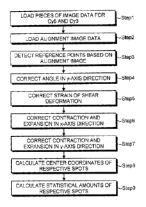
illustrated in FIG. 8. Note that Steps 1 and 2 in FIG. 8
are processes corresponding to the above-mentioned
processes.
[0053] First, at Step 1, the DNA chip is set on the
scanner and pieces of fluorescence image data of the
fluorescent dyes 0y5 and Cy3 are loaded as described above
(above-mentioned step (a)). Subsequently, at Step 2, the
laser light source 501 for Cy5 emits the excitation light
and the excitation light cut filter 507 for Cy3 is used so
as to load the alignment image while the DNA chip is kept
to be set (above-mentioned step (b)). In this process, a
configuration in which the laser light source 502 for Cy3
CA 02825727 2013-07-25
DocketNo.PTRA-13114-PCT
21
emits the excitation light and the excitation light cut
filter 508 for Cy5 is used may be employed. Alternatively,
a configuration in which another light source is prepared
and reflected light and/or scattered light of the light
from the DNA chip is/are received so as to acquire the
alignment image may be employed.
[0054] Then, the positions of the respective probes on
the pieces of fluorescence image data are determined by
using the alignment image data at and after Step 3 (above-
mentioned step (c)) so as to perform analysis.
[0055] To be more specific, first at Step 3, at least
three reference points A on the alignment image data are
detected (step (cl)). As the at least three reference
points A, coordinates of tour corners on the alignment
image can be exemplified as illustrated in FIG. 9. As a
method of detecting the coordinates of four corners, used
is edge detection using light-dark information, pattern
matching also using the light-dark information while images
at four corners are set to master images, or the like,
desirably.
[0056] Subsequently, at Steps 4 and 5, strains of the
pieces of fluorescence image data are corrected based on
the reference points A (step (c2)).
[0057] To be more specific, at Step 4, an array angle Ox
of the spots (inclination angle of a line connecting the
most adjacent spots linearly with respect to the x-axis)
with respect to the x-axis and an array angle Oy of the
spots (inclination angle of a line connecting the most
adjacent spots linearly with respect to the y-axis) with
respect to the y-axis are detected from the above-mentioned
coordinates of four corners, for example. It is desirable
that Ox and Oy take average values of angles of two line
CA 02825727 2013-07-25
DocketNoPTRA-13114-PCT
22
seyments for the corresponding directions among four line
segments connecting the coordinates of four corners. It is
to be noted that even if the reference points are three, Ox
and Oy can be calculated. Then, as illustrated in FIGS.
10(a) and 10(b), each fluorescence image data is rotated by
using the array angle Oy of the spots with respect to the
y-axis as a correction angle, so that the spots are made to
be parallel with the y-axis.
[0058] Furthermore, at Step 5, conversion (shear
deformation) is executed on the rotated image based on the
array angles Ox and Oy of the spots aligned regularly in
the two directions that have been detected as described
above and the following equations. With this, strain of
the shear deformation on the image is corrected. The
converted image is illustrated in FIG. 10(c). It is to be
noted that (x, y) in the following equation corresponds to
coordinates before conversion and (X, Y) corresponds to
coordinates after conversion. Furthermore, Oxy
corresponding to the deviation of the scanning mechanism of
the scanner (orthogonal degree of the reference axes of the
scanning mechanism) is obtained by subtracting the array
angle Oy of the spots with respect to the y-axis from the
array angle Ox of the spots with respect to the x-axis as
illustrated in Equation 4.
[0059]
rX 1 OV.K\
(3)
Y) tan Oxy
[0060]
Oxy = Ox - Ay (4)
[0061] Furthermore, when the DNA chip 1 is a resin mold,
the resin expands with moisture absorption and temperature
change in the hybridization process and the washing process
CA 02825727 2013-07-25
DocketNo.PTRA-13114-PCT
23
in some cases. Depending on the processing time in each
process, the resin expands by several tens pm in some cases
to give an influence on accuracy of alignment.
[0062] For this reason, the chip lengths in the x-axis
direction and in the y-axis direction are calculated from
the above-mentioned coordinates of four corners at Steps 6
and 7, for example, and each fluorescence image data is
contracted such that the chip length is identical to a
designed value.
[0063] Subsequently, alignment is performed on each
fluorescence image data on which rotational correction,
shear deformation correction, and contraction correction
have been performed as described above. The pieces of
positional information of the respective spots on the
template that has been stored in the analysis definition
file previously indicate center coordinates of the spots
while an upper left corner of the chip is set to a point of
origin, for example. Alignment can be performed on each
image after the contraction correction has been performed
at Step 7 as illustrated in FIGS. 11(b) and 11(c) by
calculating each spot frame while setting the coordinates
of the upper left corner to the point of origin, for
example (Step 8). It is to be noted that FIG. 11(b)
illustrates an image indicating a result of the alignment
performed on the fluorescence image data of Cy3 and FIG.
11(c) illustrates an image indicating a result of the
alignment performed on the fluorescence image data of Cy5.
Furthermore, FIG. 11(a) illustrates an image indicating a
result of the alignment perfoimed on the alignment image
data obtained at Step 2 as a reference. In the drawings,
inner portions of circles drawn by dashed lines are
detection areas defined by the template.
[0064] Thereafter, at Step 9, statistical amounts such
CA 02825727 2013-07-25
DocketNo.PTRA-13114-PCT
24
as average values, median values, and standard deviations,
for the signal intensities of pixels within the spot radius
are calculated from the center coordinates of the
respective spots that have been obtained at Step 8. Then,
the respective pieces of numerical data in addition to
block numbers to which the spots belong, matrix numbers of
the spots, and arranged probe DNA names are output as files.
[0065] It is to be noted that the order of the above-
mentioned Steps 1 and 2 may be switched in the process as
illustrated in FIG. 8.
[0066] Furthermore, the four corners of the DNA chip are
molded to be rounded in order to improve fluidity of the
specimen at the time of the hybridization in some cases.
The reference points A are desirably detecLed based on the
coordinates of points on a contour of the DNA chip when the
reference points A are detected at Step 3.
[0067] That is to say, as illustrated in FIGS. 12, a
contour point detection window (observation region) Wy
containing a contour extending to the x-axis direction
substantively and a contour point detection window Wx
containing a contour extending to the y-axis direction
substantively are set in the vicinity of each of the four
corners of the DNA chip. Then, a contour reference point a
corresponding one point on the contour of the DNA chip is
detected on each of the contour point detection windows Wx
and Wy. Thereafter, coordinates of the reference point A
corresponding to the corner of the DNA chip are calculated
from the y coordinate of the contour reference point a on
the window Wy and the x coordinate of the contour reference
point a in the window Wx. This processing is performed for
four corners, for example.
[0068] Furthermore, when only one contour point
detection window Wx and one contour point detection window
CA 02825727 2013-07-25
DocketNo.PTRA-13114-PCT
Wy are set for each of the four corners, if the DNA chip is
fixed to a fixing jig of the scanner obliquely, error is
generated between the position of the reference point A to
be detected and the position of the reference point A
5 detected actually as illustrated in FIG. 13(a) and FIG.
13(b). Note that in FIG. 13(b), the portion surrounded by
the two-dot chain line in FIG. 13(a) is enlarged. Due to
the error, the spots cannot be aligned desirably.
[0069] In order to solve this, in the invention, it is
10 preferable that at least four contour point detection
windows Wx and four contour point detection windows Wy,
that is, equal to or more than eight contour point
detection windows in total be set. To be more specific, as
illustrated in FIG. 13(c), it is preferable that at least
15 two contour point detection windows Wx (1301 and 1302) and
at least two contour point detection windows Wy (1303 and
1304) be set for each of the four corners (step (c11)).
[0070] For each of the four corners, at least two
contour point detection windows Wx (1301 and 1302) are
20 paired as a set and an approximate straight line with
respect to a plurality of contour reference points a on the
set is obtained, and at least two contour point detection
windows Wy (1303 and 1304) are paired as a set and an
approximate straight line with respect to a plurality of
25 contour reference points a on the set is obtained (step
(c12)). An intersecting point of two approximate straight
lines obtained in this manner is obtained so as to be set
as the reference point A (step (c13)).
[0071] With this, the reference points A can be detected
with high accuracy even when the chip is fixed obliquely.
[0072] In the invention, the reference points A are not
necessarily required to be obtained on the four corners and
it is sufficient that the reference points A are obtained
CA 02825727 2013-07-25
DocketNoPTRA-13114-PCT
26
on the three corners.
[0073] Furthermore, when the reference points A are
detected as described above, measurement error is generated
if scratches or dusts are present on the detector. Due to
this, even if four reference points A corresponding to four
corners of the substrate are detected, a shape formed by
connecting these four reference points A is not a
parallelogram (including rectangle shape and square shape)
but a quadrangular shape such as a trapezoidal shape in
some cases. The correction of the shear deformation strain
at the subsequent processing Step 5 is performed with the
assumption that the shape formed by the detected reference
points is the parallelogram. This arises a risk that the
spots cannot be aligned desirably in the above-mentioned
case.
[0074] For solving this, in the invention, as
illustrated in FIG. 14, the quadrangular shape formed by
the four reference points A 600 to 603 detected once is not
the parallelogram (including rectangle shape and square
shape), it is preferable that the shape be made to
approximate to a parallelogram and the vertices of the
approximated parallelogram be set as the reference points A
700 to 703 again.
[0075] For making the quadrangular shape formed by the
four reference points A 600 to 603 detected first
approximate to a parallelogram, an average of slopes of two
line segments 1401 and 1402 as opposite sides and the
respective intermediate points of the line segments 1401
and 1402 are obtained. Then, two straight lines passing
through the intermediate points and having the average
slope are obtained. This processing is performed for other
two line segments in the same manner and the intersecting
points of the obtained four straight lines are set as the
CA 02825727 2013-07-25
DocketNo.PTRA-13114-PCT
27
reference points A 700 to 703 again after approximation to
the parallelogram. With this, even if the measurement
error is generated on the reference points detected once,
alignment can be performed with high accuracy.
[0076] In the invention, the fluorescence image data
obtained based on the gene expression is processed in the
above manner to acquire desired numerical data. The
various types of numerical data thus obtained are used for
analyzing presence of the gene to be obtained, expression
of a certain gene, or the degree of expression of the gene,
and so on.
[0077] Furthermore, in the above-mentioned analysis of
the DNA chip, correction and alignment of the image are
performed by using irregularities of the DNA chip.
Positioning processing of the detection areas arranged on
the substrate of the DNA chip can be also executed with
high accuracy even for an image on which the sample
extracted from the specimen contains a small amount of DNAs
and spots emitting light are less and an image obtained by
a reading device in which accuracy of the scanning
mechanism is bad.
[0078] In the above-mentioned embodiment, described has
been the embodiment of the DNA chip on which DNAs have been
spotted onto the microarray. The invention can be also
applied to a chip on which RNAs, proteins, small specimens,
low-molecular compounds, cells, or the like are spotted.
[0079] For example, the same method can be used even in
the case where proteins (antibodies) instead of the DNAs
are immobilized onto the substrate of the DNA chip having
the irregular shape as described above and presence or
absence of reaction with a specimen and quantification are
detected with fluorescence. There are the case where
proteins present in a sample cell lysate are labeled with
CA 02825727 2013-07-25
DocketNo.PTRA-13114-PCT
28
Cy5 and proteins present in a control cell lysate are
labeled with Cy3 and they are mixed to react with the
antibody array, and the method where proteins are labeled
with biotin instead of the fluorescence and they are bonded
to the antibody array, and then, a signal is sensitized by
using enzyme-labeled avidin. Even in these cases, the
invention makes it possible to perform alignment with high
accuracy and output various types of numerical data of
fluorescence intensities as files. In the case of the RNA
array, the method can be used when hybridization of the
RNAs immobilized onto the substrate having the irregular
shape and the fluorescence-labeled DNAs or RNAs is detected
with fluorescence. In the cases of the small specimens and
the cell arrays, the invention can be applied when the
bonding reaction between the small specimens or the cells
immobilized onto the substrate having the irregular shape
and the fluorescence-labeled specimen (for example,
antibody) is detected with fluorescence.
Reference Signs List
[0080] 1 DNA CHIP
2 SUBSTRATE
3 SPOT
4 SCANNER
5 SCANNER CONTROL PC
6 IMAGE SERVER
7 ANALYSIS PC
8 DNA CHIP IMAGE FILE
9 ANALYSIS DEFINITION FILE
10 NUMERICAL DATA FILE
501 LASER LIGHT SOURCE (FOR Cy5)
502 LASER LIGHT SOURCE (FOR Cy3)
503 PERFORATED MIRROR
504 OBJECTIVE LENS
CA 02825727 2013-07-25
DocketNo.PTRA-13114-PCT
29
505 FLUORESCENCE FROM FLUORESCENT MOLECULES
506 LASER BEAM REFLECTED AND/OR SCATTERED FROM
SUBSTRATE SURFACE
507 EXCITATION LIGHT CUT FILTER (FOR Cy3)
508 EXCITATION LIGHT CUT FILTER (FOR Cy5)
509 IMAGING LENS
510 PINHOLE
511 DETECTOR
512 MIRROR
513 MIRROR
600 TO 603 REFERENCE POINT A DETECTED ONCE
700 TO 703 REFERENCE POINT A AFTER APPROXIMATION TO
PARALLELOGRAM
1101 REFERENCE POINT OF ALIGNMENT IMAGE
1102 CALCULATED SPOT FRAME
1301, 1302 CONTOUR POINT DETECTION WINDOW WX
1303, 1304 CONTOUR POINT DETECTION WINDOW WY
1401 TO 1402 LINE SEGMENT