Note: Descriptions are shown in the official language in which they were submitted.
CA 02826268 2013-09-06
ELECTROSTATIC DISCHARGE ARRANGEMENT FOR AN ACTIVE
MATRIX DISPLAY
FIELD OF THE DISCLOSURE
[0001] The present disclosure generally relates to electronic displays, and
more particularly to
protecting circuitry of active matrix displays from electrostatic discharge.
BACKGROUND
[0002] Electronic devices are prone to damage from Electrostatic Discharge
(ESD). Mobile
electronic devices are sometimes exposed to conditions that cause generation
of electrostatic
potentials that can cause ESD damage, particularly in miniaturized electronic
components used
in mobile devices. ESD is able to damage many electronic components of an
electronic device
including simple circuits, e.g. conductive traces within the device, and also
complex logic
circuits such as integrated circuit components.
[0003] As one example, a Liquid Crystal Display (LCD) is typically a
relatively large
component on an electronic device, particularly a mobile electronic device. An
LCD typically
includes relatively sensitive electronic components that are integrated into
the display, such as
Thin Film transistors (TFTs), driver integrated circuits (ICs), and
transparent conductive traces to
drive each pixel. The transparent conductive traces that drive each pixel are
generally thin traces
that are sometimes located close to one another.
[0004] As a large surface, the glass panel of the LCD is able to be
parasitically coupled to other
metals or conductors in the device such that electrostatic potentials will
couple those conductors.
An electrostatic potential generated on the glass panel of the LCD is able to
generate an electrical
44408-CA-PAT
- 1
CA 02826268 2013-09-06
current that can travel through the circuits on the Glass Panel, such as thin
conductive traces, the
driver IC, etc., that are able to damage to those components.
[0005] Therefore, the reliability of glass panel displays is limited by
electrostatic potentials that
are able to be generated on the glass panel and that are able to be discharged
through components
of the display.
BRIEF DESCRIPTION OF THE DRAWINGS
[0006] The accompanying figures where like reference numerals refer to
identical or
functionally similar elements throughout the separate views, and which
together with the detailed
description below are incorporated in and form part of the specification,
serve to further illustrate
various embodiments and to explain various principles and advantages all in
accordance with the
present disclosure, in which:
[0007] FIG. 1 illustrates a handheld electronic device in accordance with one
example;
[0008] FIG. 2 illustrates a Liquid Crystal Display (LCD) layer side view,
according to one
example;
[0009] FIG. 3 illustrates a color filter glass top view, according to one
example;
[0010] FIG. 4 illustrates an example spark gap point set region detail,
according to one example;
[0011] FIG. 5 illustrates an electrostatic discharge structure formation
process, according to one
example; and
[0012] FIG. 6 is a block diagram of an electronic device and associated
components in which the
systems and methods disclosed herein may be implemented.
44408-CA-PAT
- 2 -
CA 02826268 2013-09-06
DETAILED DESCRIPTION
[0013] As required, detailed embodiments are disclosed herein; however, it is
to be understood
that the disclosed embodiments are merely examples and that the systems and
methods described
below can be embodied in various forms. Therefore, specific structural and
functional details
disclosed herein are not to be interpreted as limiting, but merely as a basis
for the claims and as a
representative basis for teaching one skilled in the art to variously employ
the disclosed subject
matter in virtually any appropriately detailed structure and function.
Further, the terms and
phrases used herein are not intended to be limiting, but rather, to provide an
understandable
description.
[0014] The terms "a" or "an", as used herein, are defined as one or more than
one. The term
plurality, as used herein, is defined as two or more than two. The term
another, as used herein, is
defined as at least a second or more. The terms "including" and "having," as
used herein, are
defined as comprising (i.e., open language). The term "coupled," as used
herein, is defined as
"connected," although not necessarily directly, and not necessarily
mechanically. The term
"configured to" describes hardware, software or a combination of hardware and
software that is
adapted to, set up, arranged, built, composed, constructed, designed or that
has any combination
of these characteristics to carry out a given function. The term "adapted to"
describes hardware,
software or a combination of hardware and software that is capable of, able to
accommodate, to
make, or that is suitable to carry out a given function.
[0015] The following examples describe light transmissive electrostatic
discharge structures that
are incorporated on light transmissive panels. In the following description,
the term light
transmissive refers to substances or structures thought which transfer is able
to be transferred.
44408-CA-PAT
-3 -
CA 02826268 2013-09-06
The term light transmissive, as used below, includes material that is
transparent or translucent.
In the following discussion, material that is described as light transmissive
is able allow light to
transfer through the material with or without distortion and with or without
appreciable
attenuation. Light transmissive material in some examples is further able to
perform color
filtering of light being transmitted through that material.
[0016] The below described systems and methods are described with reference to
an example
application that includes glass panel displays, such as a Liquid Crystal
Display (LCD). As is
understood for conventional LCDs, a liquid crystal display structure includes
a number of pixels
that are used to create an image to be displayed to a user. A color LCD
generally divides each
pixel into sub-pixels, where each pixel has a sub-pixel that emits or reflects
light of a particular
color for that pixel.
[0017] The display of one example consists of two glass layers sandwiching
Liquid Crystal
material. In one example, these two glass layers perform the functions of
similar layers of a
conventional LCD. In one example, the top glass layer in the display structure
is a Color Filter
(CF) glass that includes color filters used to provide color filtering of
light that is emitted or
reflected by each sub-pixel of the display. The bottom glass layer in one
example is what is
referred to as a Thin-Film Transistor (TFT) glass. The TFT glass layer of an
LCD includes
circuitry and electronic components used to drive the liquid crystal cells of
each sub-pixel.
[0018] The color filter glass in this example has a layer of substantially
transparent Indium Tin
Oxide (ITO) material that is a light transmissive conductive material used to
form a light
transmissive conductive area that provides a common voltage, or VCOM,
potential to one end of
each liquid crystal cell of the display. In one example of a liquid crystal
display with a common
44408-CA-PAT
- 4
CA 02826268 2013-09-06
voltage, or VCOM, potential that is applied to one side of each liquid crystal
cell by an electrical
conductor held at the VCOM potential, the liquid crystal cells are controlled
by an individualized
voltage applied to an opposite side of each liquid crystal cell. In one
example, a VCOM
electrical potential is maintained on an electrically conductive structure,
referred to herein as a
VCOM layer, that extends across all liquid crystal cells of the liquid crystal
display. As is
understood by practitioners of ordinary skill in the relevant arts, ITO is a
translucent material that
appears to be substantially transparent when it is applied as a thin layer on
a surface. As is
further understood by practitioners of ordinary skill in the relevant arts, a
VCOM layer
consisting of a light transmissive layer of ITO that is maintained at a VCOM
potential is formed
on a side of a color filter glass of a liquid crystal device that is in
contact with the liquid crystal
cells. In an example described below, the VCOM ITO layer is formed so as to
further provide an
electrostatic potential discharge structure for the display structure. In
further examples, light
transmissive conductive material any electrically conductive material that
allows light to pass
through the material in any manner. In some examples, light transmissive
conductive material
includes different materials that are considered to be transparent or other
materials that are
considered translucent.
Light transmissive conductive materials further include different
electrically conductive materials that also exhibit various degrees of
conductivity.
[0019] In one example, the layer of ITO transparent conductor on the color
filter glass includes a
number of spark gap geometrical features along its edge. These spark gap
geometrical features
in one example are located along the outer edge of the VCOM ITO layer. These
spark gap
geometrical features on the edge of the VCOM ITO layer are located in
proximity to, but are
conductively isolated from, an electrostatic discharge conductor that is
maintained at an
electrostatic discharge voltage potential, such as a system ground electrical
potential. In one
44408-CA-PAT
-5 -
CA 02826268 2013-09-06
example, the spark gap geometrical features formed on the VCOM ITO layer are
located in
proximity to corresponding features on the electrostatic discharge conductor
such that a spark
gap is formed between the VCOM ITO layer and the electrostatic discharge
conductor. The
relative locations of the spark gap features of the VCOM ITO layer and the
electrostatic
discharge conductor are chosen so as to result in a breakdown voltage across
the spark gap that
occurs when the electrostatic potential between the VCOM ITO layer and the
electrostatic
discharge conductor exceeds a certain voltage. In one example, the features of
the VCOM ITO
layer and the electrostatic discharge conductor are configured such that an
electrostatic
breakdown and discharge occurs when the voltage between the VCOM ITO layer and
the
electrostatic discharge conductor exceeds a few hundred volts. This
configuration causes the
electrostatic discharge surge current to pass through to the electrostatic
discharge conductor,
which is able to be held at a ground potential, without damaging other
circuits on display.
[0020] In this discussion, electrostatic breakdown refers to any transfer of
electrons between or
among two or more electrically conductive structures, where the transfer is
caused by a
breakdown of electrically insulating properties of materials or a vacuum that
separates the two or
more electrically conductive structures. In general, electrostatic breakdown
occurs when the
electrical voltage potential between two electrical conductors of a particular
geometric
configuration exceeds a discharge breakdown voltage. The discharge breakdown
voltage of a
particular pair of electrical conductors is dependent upon the physical
configuration of those
structures, particularly in the vicinity of their closest point. The discharge
breakdown voltage is
sometimes referred to as being a "determined voltage" because the discharge
breakdown voltage
is determined by the physical configuration of the two or more electrically
conductive structures
that are separated by an insulating material and by the conductive properties
of the electrically
44408-CA-PAT
- 6 -
,
CA 02826268 2013-09-06
conductive material in conjunction with the electrical properties of the
insulating material
separating them.
[0021] In one example, the electrostatic discharge conductor surrounds the
VCOM ITO layer on
the color filter glass. Advantages of this design include forming the
electrostatic discharge
conductor as part of the same ITO layer formation process that creates the
VCOM ITO layer.
The electrostatic discharge conductor in one example is maintained at a static
discharge
potential, which is a voltage potential to which electrostatic charges that
build up in one or more
parts of a device are discharged. In the case of a static discharge potential
that is a system
ground potential for the device, the electrostatic discharge conductor is
simply routed to the
electrical ground connection on display driver IC, to another ground location
on the display, to
any conductor that is held at ground potential, or to any combinations of
these. As is generally
understood, a "ground" potential of a device is an electrical potential used
as a reference for
other voltage potentials in the device and is not necessarily related to an
"earth" potential of the
physical earth in the vicinity of the device.
[0022] The design of one example allows the incorporation of these spark gap
structures into the
glass panel display using conventional manufacturing techniques without adding
manufacturing
complexity. The below described displays are able to be manufactured using
conventional
techniques and fabrication equipment, thereby resulting in a minimal cost
impact. In one
example, both the VCOM layer and the electrostatic discharge conductor are
formed of light
transmissive ITO material and are able to be deposited or otherwise placed on
a glass layer by
the same formation process. The manufacturing processes involved in forming
ITO regions on a
glass substrate allow economical fabrication of light transmissive conductive
areas with high
location tolerances that allow the formation of spark gap structures with
highly precise and small
44408-CA-PAT
- 7 -
CA 02826268 2013-09-06
dimensions. In one example, ITO fabrication techniques allow economical
formation of ITO
conductive areas with dimension tolerances of less than 1.5 gm. As is
understood by
practitioners of ordinary skill in the relevant arts, the term dimension
tolerance generally refers
to the accuracy with which components, such as edges of the ITO regions
discussed above, are
able to be located during a manufacturing process. In one example, the term
dimension tolerance
refers to the variation of actual location of a component in a manufactured
product, such as the
edge of the ITO region, relative to the location specified for that component
by the design of the
product. The economical formation of such precisely located conductors allows
the economical
fabrication of spark gap structures with narrow gaps and correspondingly low
breakdown
voltages as compared to metallic conductive trace fabrication techniques,
which generally
provide less precise trace location accuracies. Forming such small, precisely
located spark gap
structures along one or more edges of a transparent, conductive area on a
display allows for
precise control of the electrostatic voltage at which conduction across the
spark gap breaks down
and therefore the highest electrostatic potential that will be present on the
transparent conductive
area. In some examples, the electrostatic discharge conductor is formed of
another conductive
material, such as a metallic material, that is deposited in proximity to the
transparent conductive
area.
[0023] In the following discussion, components that are referred to as being
"conductive"
generally refer to components that are electrically conductive and are able to
further have a
reactive component. It is to be understood that different components having a
wide range of
conductivity, resistivity, inductance, or admittance, are encompassed within
the term conductive.
Conductive materials are further able to exhibit other forms of conductivity,
such as heat
conductivity. It is further understood that conductive materials are able to
conduct "desired"
44408-CA-PAT
- 8 -
CA 02826268 2013-09-06
electrical energy, such as signals or electrical power, as well as the
undesired electrical energy,
such as electrostatic discharge.
[0024] In one example, the spark gap structure formed along one or more edges
of the VCOM
conductive layer is within a hermetically sealed compartment inside of an LCD
display. In such
an example, any sparking that is present as a result of electrostatic
discharge across the spark
gaps is within the hermetically sealed compartment and will not be in contact
with, for example,
flammable gasses or other gasses present in the vicinity of the display.
[0025] Incorporating electrostatic discharge spark gap structures onto an edge
of a transparent,
conductive area of a transparent or translucent panel, such as a front panel
of a display, provides
an effective electrostatic field that is located in an area of a device that
is likely to be in contact
with electrostatic charge sources. One application of the below described
electrostatic discharge
structures is incorporating these structures into an LCD, including LCDs that
further incorporate
touch screen user interface functionality. Utilizing the already present VCOM
transparent
conductive layer as a conductive "screen" for an electrostatic discharge
structure provides
electrostatic protection across a relatively large area where a user is likely
to touch the electronic
device with a finger or conductive element. A user is at times likely to
accumulate a relatively
high static electric potential, particularly in conditions of low humidity.
Electrostatic charge
accumulated on a user is likely to couple, particularly through capacitive
coupling, to the VCOM
transparent conductive layer of an LCD display when the user touches the
display as is common
in many uses of a device with a display. Forming such an already present VCOM
layer with
additional features along one or more edges that function as spark gap
elements and that are in
proximity to an electrostatic discharge conductor allows the electrostatic
potential that couples to
the VCOM layer from a user or other source to be harmlessly dissipated without
damaging
44408-CA-PAT
- 9 -
CA 02826268 2013-09-06
internal components to which elements of the display are electrically coupled.
Using the VCOM
layer as an electrostatic shield for the display further operates to protect
the active and passive
components that are present throughout the display structure, such as the Thin
Film Transistors
(TFTs) that are located across the area of the display.
[0026] Adding electrostatic discharge features to a VCOM layer and forming an
electrostatic
discharge conductor in proximity to those additional features provides a cost
effective
electrostatic discharge structure that does not use additional components.
Incorporating
electrostatic discharge structures into already present layers of a display
obviates the expense of
including separate electrostatic discharge components into the device,
simplifies manufacturing
complexity and thereby improves manufacturing yields of such display devices.
The lack of
additional electrostatic discharge devices further obviates a need to increase
the size of the
display to accommodate the additional electrostatic devices. The effective
electrostatic
protection provided by the VCOM conductive layer, which generally extends over
all liquid
crystal cells of a display, also increase the reliability of devices
incorporating such displays by
protecting such devices from damage due to electrostatic discharge through
sensitive
components within the device.
[0027] FIG. 1 illustrates a handheld electronic device 100 in accordance with
one example. The
portable electronic device 100 in this example is a handheld smartphone that
supports cellular
voice communications and also data communications with a central network. In
one example,
the electronic device 100 performs data communications with a wireless network
to support
accessing and exchanging data over the Internet. Data received by the
electronic device is
displayed on a display 106, which is able to be a color LCD device. In one
example, the display
106 presents a graphical user interface for a user to access functions and to
receive information.
44408-CA-PAT
- 10
CA 02826268 2013-09-06
In some examples, the display 106 is a touch screen type display that allows a
user to provide
input to the device by touching one or more points on the display with, for
example, a finger,
stylus, other device, or combinations of such techniques. In some examples, a
user is able to
provide various inputs by also performing one or more gestures across the
display 106, such as a
swiping gesture.
[0028] The electronic device 100 is housed within a device case 102. The
display 106 mounts
on a surface of the device case 102. An alpha-numeric keyboard 104 is also
physically coupled
to the same surface of the device case 102 as the display 106. In various
examples, the alpha-
numeric keyboard 104 is able to be a QWERTY keyboard, a numeric telephone
keypad, or any
suitable user input device.
[0029] The device case 102 further includes a number of function keys. The
illustrated device
case 102 has a first function key 120, a second function key 122, a third
function key 124, and a
fourth function key 126. These function keys are able to be associated with a
dedicated function,
such as presenting an interface to initiate a voice call whenever pressed, or
the function key is
able to be associated with different functions based upon a current operating
mode of the
electronic device 100. The device case 102 further has a directional user
input device 110, such
as a joy stick or track pad.
[0030] The display 106 in one example includes an electrostatic discharge
protection structure,
as is described below. The display 106 in one example is a touchscreen input
that allows a user
to provide user interface inputs by touching areas of the display 106, by
moving one or more
fingers or objects across the display 106, or by other touchscreen input
techniques. Although the
illustrated electronic device 100 has an alpha-numeric keyboard 104 in
addition to the display
44408-CA-PAT
- 11 -
CA 02826268 2013-09-06
106, further examples include electronic devices that do not have a large
alpha-numeric keyboard
104 but include a larger display 106, which is able to include touch screen
input functionality.
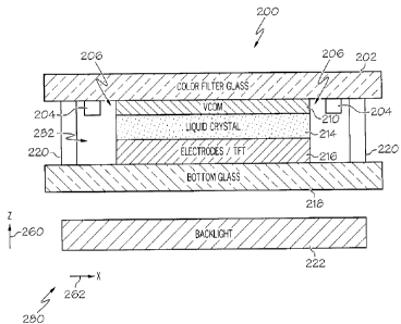
[0031] FIG. 2 illustrates a Liquid Crystal Display (LCD) layer side view 200,
according to one
example. The LCD layer side view 200 depicts several layers that are present
in an LCD device
280. The LCD layer side view 200 depicts layers as they are stacked in the
thickness of an LCD
device 280 in a 'Z' direction 260. A 'Z' direction 260 is generally
perpendicular to the display
face of the LCD device 280, such as is shown for the electronic device 100.
The LCD layer side
view 200 shows each layer extending in a horizontal 'X' direction 264.
[0032] The LCD layer side view 200 depicts the structure of an example LCD
structure that is
similar to conventionally available LCD products. One example described below
includes an
LCD display that has a design that is similar to a conventional LCD product
design except for
the formation of a specially formed conductive layer on the bottom of the
color filter glass 202.
The use of a conventional LCD display design with a specially formed
conductive layer allows
incorporation of the below described electrostatic discharge structures into
such LCD displays
with minimal cost impact and with little specialized fabrication changes.
Alternative examples
are able to include other display designs that also include many aspects of
conventional displays,
or that differ further from such conventional designs. Further, a particular
LCD device is able to
include additional layers or is able to not include all of the layers depicted
in the LCD layer side
view 200. The layers depicted in the LCD layer side view 200 are presented to
illustrate one
example design of a display described herein. Alternative designs are able to
be realized that are
consistent with the disclosures herein.
44408-CA-PAT
- 12
CA 02826268 2013-09-06
[0033] The LCD layer side view 200 depicts a liquid crystal material layer 214
located in the
middle of the LCD device 280. The liquid crystal material layer 214 includes
an individual
liquid crystal cell element for each sub-pixel of the LCD device 280. Each
liquid crystal cell
element of the liquid crystal material layer 214 is the portion of the liquid
crystal material that
corresponds to a particular sub-pixel of the liquid crystal display panel. The
sub-pixels of each
pixel in the LCD device 280 are described above in further detail with regards
to the LCD
display panel side view 200.
[0034] The individual liquid crystal cell elements of the liquid crystal
material layer 214 are
controlled by an electrode connected to a corresponding Thin Film Transistor
(TFT) contained
within the electrodes/thin film transistor (TFT) layer 216 that is deposited
on a bottom glass
layer 218. Each sub-pixel of an LCD device generally has one or more thin film
transistors that
control voltage applied to one end of each liquid crystal cell element within
the liquid crystal
material layer 214. As discussed below, a VCOM layer 210 is in contact with
the other end of
each liquid crystal cell element and is maintained at a common voltage, or
VCOM. Applying
different voltages to the liquid crystal material in each sub-pixel in the
liquid crystal material
layer 214 relative to the common voltage, or VCOM, changes the light
transmission polarization
properties of the liquid crystal material in that sub-pixel. In one example,
the controller 230
controls each of the thin film transistors on the electrodes/TFT layer 216 to
adjust the voltage
applied to each sub-pixel on the liquid crystal material layer 214. Although
the present
discussion describes a conventional electrodes/TFT layer 216, liquid crystal
cells are able to be
constructed with different structures or designs to apply electrical
potentials to individual liquid
crystal cells, groups of liquid crystal cells, or both, relative to the VCOM
potential in order to
control their appearance.
44408-CA-PAT
- 13 -
CA 02826268 2013-09-06
[0035] The LCD layer side view 200 depicts a backlight 222. Backlight 222
includes light
sources such as one or more Light Emitting Diodes (LEDs) or fluorescent light
sources. Light
generated by the backlight 222 and that passes through the bottom glass 218.
The bottom glass
218 includes a bottom polarizer to cause light emitted through the top of the
bottom glass 218 to
have a single polarization. The light emitted through the top of the bottom
glass 218 passes
through the electrodes/TFT layer 216 and enters the bottom of the liquid
crystal material 214.
The polarization of light transmitted through each sub-pixel of the liquid
crystal material layer
214 is able to be changed in varying amounts based upon the voltage applied to
the liquid crystal
material of that sub-pixel by the circuitry present on the electrodes/TFT
layer 216.
[0036] The light exiting the top of the liquid crystal material layer 214
passes through the
VCOM layer 210 and through to a color filter glass 202. In one example, the
VCOM layer 210
is a transparent or light transmissive conductive area formed by depositing
Indium Tin Oxide
(ITO) on the bottom of the color filter glass 202. The VCOM layer 210 in one
example is a
continuous conductive area that is maintained at a common voltage (VCOM) and
is a common
electrode for each sub-pixel in the liquid crystal material layer 214. The
polarization change of
light passing through each sub-pixel of the liquid crystal material layer 214
is controlled by the
voltage between the electrode connected to the TFT for that sub-pixel within
the electrodes/TFT
layer 216 and the VCOM layer 210.
[0037] In one example, an electrostatic discharge conductor 204 is formed in
proximity to the
VCOM layer 210 on the color filter glass 202. A gap 206 with a determined
pattern separates
the VCOM layer 210 from the electrostatic discharge conductor 204. As
described in detail
below, the determined pattern of the gap 206 forms at least one spark gap with
a determined
break down voltage. The design of the gap 206 between the electrostatic
discharge conductor
44408-CA-PAT
- 14 -
CA 02826268 2013-09-06
204 and the VCOM layer 210 discharges electrostatic charge potentials that
exceed the
determined break down voltage. In one example, the electrostatic discharge
conductor is formed
with a pattern of deposited ITO pattern. In other examples, the electrostatic
discharge conductor
is able to be formed by any transparent, translucent, or opaque conductive
material. An example
pattern of a VCOM layer 210 and electrostatic discharge conductor 204 that is
deposited on the
color filter glass 202 is described in detail below.
[0038] In one example, the color filter glass 202 with the VCOM layer 210 and
the discharge
conductor 204 form at least part of an electrostatic shielding panel. The
electrostatic shielding
panel of one example is a panel, generally defined in the illustrated example
by the color filter
glass 202, that includes a light transmissive conductive area defined by the
VCOM layer 210 in
this example. The light transmissive conductive area defined by the VCOM layer
210 provides
an electrostatic shield that accumulates any electrostatic energy originating
from above the color
filter glass 202 or otherwise generated on the VCOM layer 210, and inhibits
the transfer of that
electrostatic energy to elements below the VCOM layer, such as electrically
sensitive
components of the electrodes/TFT layer 216. As described, electrostatic energy
that accumulates
on the VCOM layer 210 and discharges the energy to the discharge conductor 202
prior to the
electrical potential on the VCOM layer 210 rising to a level that is able to
damage other
components.
The electrostatic shielding panel also operates to protect other electrical
components of a device to which it is mounted.
[0039] The color filter glass 202 includes a color filter pattern on a top
glass layer of the color
filter glass 202, where the color filter pattern coincides with the sub-pixel
pattern of the liquid
crystal material layer 214. The color filter glass in one example has a top
polarizer located on its
top and is typically oriented with a light transmission polarization that is
perpendicular to the
44408-CA-PAT
- 15 -
CA 02826268 2013-09-06
light transmission polarization of a bottom polarizer that is within the
bottom glass 218 in one
example. The variable amount of light polarization alteration provided for
each sub-pixel by the
liquid crystal material layer 214 allows varying amounts of light to pass
through both the pixel.
Each sub-pixel of each pixel is thereby able to emit an adjustable intensity
of its color by varying
the amount of light that passes through that sub-pixel.
[0040] The above described components of the LCD device 280 that are located
between the
color filter glass 202 and the bottom glass 218 are within a sealed
compartment 282, or a sealed
structure. The sealed compartment 282 in one example is formed by the seal 220
that joins the
color filter glass 202 and the bottom glass 218. Enclosing the LCD display
components in a
sealed compartment protects those components from contamination. In an example
where the
VCOM layer 210 and the electrostatic discharge conductor 204 are patterned so
as to create
spark gaps to discharge electrostatic potentials, the enclosed structure
operates to isolate any
sparks generated during electrostatic discharge from external elements, such
as volatile gases.
[0041] FIG. 3 illustrates a color filter glass top view 300, according to one
example. The color
filter glass top view 300 depicts an example pattern of a VCOM layer 210 that
consists of ITO
deposited on the underside of the color filter glass 202. The illustrated
color filter glass 202 is an
example of a transparent panel. As shown for this example, the VCOM layer 210
is an example
of a light transmissive conductive area that in this example is a continuous
area of ITO material
that forms a generally square or rectangular region on the color filter glass
202. The VCOM
layer 210 in this example extends across a substantial portion of a viewing
area of the transparent
panel. In this description, a light transmissive conductive area that extends
over a substantial
portion of a viewing area includes a light transmissive conductive area that
covers a sufficient
portion of a light transmissive panel so as to cause electrostatic voltage
potentials accumulating
44408-CA-PAT
- 16 -
CA 02826268 2013-09-06
in the viewing area of the light transmissive panel to couple to the light
transmissive conductive
area. In various examples, the light transmissive conductive area is able to
extend across most of
the viewing area but not reach the edges of the viewing area, or the light
transmissvie conductive
area substantially covering the viewing area is able to be perforated or
otherwise not cover the
entirety of the viewing area. In the illustrated example, the viewing area of
the transparent panel
corresponds to the pixels in the liquid crystal layer 214. In further
examples, the viewing area of
a light transmissive panel is an area through which light is transferred. The
transfer of light
through a viewing area is able to be for purposes of viewing images through
the light
transmissive panel, for conveying illumination through the light transmissive
panel, or for any
other purpose.
[0042] The VCOM layer 210 in the illustrated example extends over all of the
pixels of the
liquid crystal layer so as to from a Common Voltage (VCOM) potential along the
top of each
sub-pixel liquid crystal cell. An electrode/TFT glass 216 is also depicted as
being below the
color filter glass 202. As described above, the liquid crystal layer is
sandwiched between the
electrode/TFT glass 216 and the color filter glass 202. The liquid crystal
layer is not depicted in
the color filter glass top view 300 in order to more clearly depict aspects of
the features being
described.
[0043] The VCOM layer 210 is shown to have an outside perimeter with four
edges, a left edge
330, a bottom edge 332, a right edge 334 and a top edge 336. An electrostatic
discharge
conductor 204 is located in proximity to part of the outside perimeter of the
VCOM layer 210,
specifically along the left edge 330, the bottom edge 332 and the right edge
334. As shown, the
VCOM layer 210 is separated from and ohmically isolated from the electrostatic
discharge
conductor 204 by a gap 206. In this example, the VCOM layer 210 is also
ohmically isolated
44408-CA-PAT
- 17 -
CA 02826268 2013-09-06
from any other conductor that is at a static discharge potential. In the
following discussion, two
conductors are referred to as being ohmically isolated when an electrically
conductive path does
not exist between the two conductors. Ohmically isolated conductors are
separated by normally
insulating material, such as air, other non-conductive materials, active
components, or
combinations of these, such that electrons do not normally flow between the
two conductors. It
is to be understood, however, that ohmically isolated conductors are able to
be electrically
connected through, for example, active circuits such as power supplies in such
a way that
electrical signals are not normally conveyed betweent the ohmically isolated
conductors.
Ohmically isolated conductors, however, are able to be separated by material
that allows a
discharge of electrical potential by breaking down at a voltage such that an
arc is formed that
allows electrons to flow from one conductor to another. In general, two
ohmically isolated
conductors are able to be separated from one another in a manner that forms a
spark gap within
the insulating material, such as air, that is between the two conductors,
where the dimensions of
the spark gap and the characteristics of the insulating material result in a
defined discharge
breakdown voltage, which is the voltage between the two conductors at which a
discharge of
static electric charge occurs between the two conductors by an arc that forms
across the
insulating material.
[0044] In operation, the static electric potential that accumulates on the
VCOM layer 210 is
discharged across the gap 206, which consists of air or other insulating
material, to the
electrostatic discharge conductor 204. The electrostatic discharge conductor
in this example is
connected to a power supply connection that is at a static discharge
potential, such as a system
electrical ground potential or other voltage.
44408-CA-PAT
- 18
CA 02826268 2013-09-06
[0045] In various examples, a determined discharge breakdown voltage across
the gap 206 is
able to be set to various values based upon the conductivity and geometries of
the VCOM layer
210, the electrostatic discharge conductor 204, and the material in the gap
206 (such as air, a
vacuum, or other insulating material). In one example, one or both of the
edges of the VCOM
layer 210 and the electrostatic discharge conductor 204 are formed with
geometric features that
facilitate the discharge electrostatic accumulations across the gap 206. These
geometric features
are referred to herein as spark gap points. Although these geometric features
are referred to as
"points," these geometric features are generally able to be formed with any
shape, such as curves
or other geometric constructions, that do not necessarily create a sharp
point. In various
examples, the geometries of and spacing between conductive area spark gap
points of the VCOM
layer 210 and the discharge conductor 204 are able to be selected such that
these conductors have
an electrostatic breakdown voltage of less than 1000 volts. In other words,
the electrostatic
potential that is formed between the VCOM layer 210 and the electrostatic
discharge conductor
204 in normal operations will not exceed 1000 volts because electrostatic
potentials above that
level will result in an electrostatic breakdown between those conductors and a
discharge of the
accumulated electrostatic potential. In further examples, the geometries of
and spacing between
conductive area spark gap points of the VCOM layer 210 and the discharge
conductor 204 are
able to be selected such that these conductors have an electrostatic breakdown
voltage of, for
example, less than 10,000 volts in one example, or less than 200 volts in
another example. The
precise light transmissive conductive layer formation that is available with
ITO creation
techniques allows the formation geometries of and spacing between conductive
area spark gap
points of the VCOM layer 210 and the discharge conductor 204 that support an
electrostatic
breakdown voltage of less than 200 volts.
44408-CA-PAT
- 19
CA 02826268 2013-09-06
[0046] In the illustrated example, a number of conductive area spark gap
points are located along
one side of the gap on the left edge 330, the bottom edge 332 and the right
edge 334 of the
VCOM layer 210. The electrostatic discharge conductor 204 that adjoins the
left edge 330, the
bottom edge 332 and the right edge 334 of the VCOM layer 210 also has
corresponding
discharge locations that consist of respective discharge spark gap points. In
the illustrated
example, each conductive area spark gap point has a respective discharge
location, which
includes a discharge spark gap point in this example, that is located in
proximity to and across
the gap 206 from each conductive area spark gap point of the VCOM layer 210.
An example
spark gap point set 310, which includes one conductive area spark gap point
and one discharge
spark gap point, is described in detail below. In the present discussion, a
discharge location
includes a location on any electrically conductive structure where
electrostatic discharge to a
second electrical conductor occurs to another conductor, where the other
conductor is ohmically
isolated from the electrically conductive structure with the discharge
location. In general, two or
more ohmically isolated electrically conductive structures that are configured
to support
electrostatic discharge between or among each other will each have their own
discharge location,
and a particular electrostatic discharge between two electrical conductors
generally defines one
discharge location on each of the electrical conductors.
[0047] The color filter glass top view 300 depicts a driver IC 320. The driver
IC 320 in one
example is incorporated into the LCD device 280. The driver IC 320 in one
example generates
control signals that drive each pixel and sub-pixel in the LCD device 280. The
driver IC 320
generates signals that drive the TFTs of the electrodes/TFT layer 216,
discussed above. Signals
driving the rows and columns of sub-pixels in the LCD device 280 are not shown
in this
illustration in order to simplify aspects of the electrostatic discharge
structure present in this
44408-CA-PAT
- 20 -
CA 02826268 2013-09-06
=
example. In addition to driving each sub-pixel of the LCD device 280, the
driver IC 320
generates a VCOM voltage level to be used as a potential for one end of each
liquid crystal cell
within the liquid crystal layer 214. In general, the driver IC 320 includes
electrostatic protection
circuits that protect components of the driver IC 320 from electrostatic
potentials up to several
thousand volts. The electrostatic discharge structures described herein that
are incorporated into
the VCOM layer 210 in one example are dimensioned to discharge electrostatic
voltage
potentials of several hundred volts. Discharging electrostatic potentials on
the VCOM layer 210
of several hundred volts operates in conjunction with the electrostatic
protection incorporated
into the driver IC 320, and other devices coupled to the LCD device 280, to
prevent damage due
to electrostatic discharge.
[0048] The driver IC 320 in one example also includes one or more terminals
that are at a static
electric discharge voltage potential. In one example, the static electric
discharge voltage
potential is a system ground voltage potential. In further examples, the
static electric discharge
voltage potential is able to be any fixed or varying voltage potential
relative to a system ground
voltage potential. In general, the system ground voltage potential of a
particular system is
maintained by a power supply connection that is able to accept an amount of
static electric
charge that is expected to accumulate on the VCOM layer 210 of the particular
system. In
various examples, a "ground voltage potential" is not related to an actual
"earth" electrical
potential. In an example of a portable, battery operated electrical device, a
ground voltage
potential is an electrical potential that serves as a reference for other
power supply voltages,
signal voltages, and other voltages. In such a portable, battery powered
device, the ground
voltage potential of that device is not electrically coupled to an earth
ground potential, and in fact
44408-CA-PAT
- 21 -
,
CA 02826268 2013-09-06
,
the ground voltage potential of the battery powered device is able to vary
relative to the earth
ground potential in the vicinity of the device.
[0049] FIG. 4 illustrates an example spark gap point set region detail 400,
according to one
example. The spark gap region detail 400 depicts an expanded view of the above
described
example spark gap point set 310. The example spark gap point set region detail
400 depicts a
VCOM layer portion 402, which is an example of a portion of a light
transmissive conductive
layer, and a discharge conductor portion 404. A conductive area spark gap
point 408 is
illustrated as a pointed protrusion from the illustrated VCOM layer portion
402. Conductive area
spark gap points in further examples are able have any configuration that is
in proximity to a
discharge conductor such that the geometry of the conductive area spark gap
point and the
discharge conductor support electrostatic breakdown at less than a determined
voltage. A
discharge spark gap point 406 is illustrated as a pointed protrusion from the
discharge conductor
portion 404. The discharge spark gap point 406 is an example of a discharge
location of a
discharge conductor 204. Discharge locations in further examples are able have
any
configuration that is in proximity to a conductive area spark gap point 408
such that the
geometry of the discharge location and the spark gap point support
electrostatic breakdown at
less than a determined voltage.
[0050] The example spark gap point set region detail 400 illustrates that the
example spark gap
point set 310 includes a pair of spark gap points, i.e., the discharge spark
gap point 406 and the
conductive area spark gap point 408, extending from their respective surfaces
into the gap 206.
The discharge spark gap point 406 and the conductive area spark gap point 408
are constructed
such that these two spark gap points are opposite one another and are located
in proximity to
each other such as to form a static electric discharge gap 410. In one
example, the dimension of
44408-CA-PAT
- 22 -
CA 02826268 2013-09-06
the static electric discharge gap 410, in combination with the geometry of the
discharge spark
gap point 406 and the conductive area spark gap point 408, supports
electrostatic breakdown at
less than a determined voltage between the discharge spark gap point 406 and
the conductive
area spark gap point 408.
[0051] FIG. 5 illustrates an electrostatic discharge structure formation
process 500, according to
one example. The electrostatic discharge structure formation process 500 is an
example of part
of a Liquid Crystal Display (LCD) manufacturing process that creates a VCOM
layer 210 and an
electrostatic discharge conductor 204 that include the above described spark
gaps.
[0052] The electrostatic discharge structure formation process 500 beings by
forming, at 502, a
light transmissive conductive area with at least one conductive area spark gap
point on a light
transmissive panel. In the following description, the light transmissive panel
is a transparent
panel. In further examples, light transmissive panels are able to be
translucent panels or panels
the perform color filtering. The formation of the light transmissive
conductive area in one
example is a formation of a VCOM layer of a Liquid Crystal Display (LCD). In
that example,
the light transmissive conductive area is deposited on a color filter glass
panel, such as is
described above. In addition to the creation of a VCOM layer is as found in
some conventional
LCDs, the light transmissive conductive area in this example is formed with at
least one
conductive area spark gap point. As is discussed above with regards to FIG. 3,
a light
transmissive conductive area is able to be formed with a large number of
conductive area spark
gap points that are formed along one or more edges of the light transmissive
conductive area. In
one example, the light transmissive conductive area is formed by depositing on
the color filter
glass a layer of Indium Tin Oxide (ITO) material with a thickness able to
conduct anticipated
44408-CA-PAT
- 23
CA 02826268 2013-09-06
electrical currents encountered by one or both of LCD operations and discharge
of electrostatic
potential that is able to accumulate on the VCOM layer.
[0053] The electrostatic discharge structure formation process 500 continues
in one example by
forming, at 504, a discharge conductive strip that at least partially
surrounds the light
transmissive conductive area. In one example, the discharge conductive strip
is conductively
connected to one or more discharge spark gap points that are located in
proximity to the
conductive area spark gap points that are conductively coupled to the light
transmissive
conductive area formed above. In one example, the discharge conductive strip
is formed with
the one or more discharge spark gap points extending from an edge of the
discharge conductive
strip that is opposite the light transmissive conductive area.
[0054] Although the above description describes forming the light transmissive
conductive area
and then forming the discharge conductive strip, further examples are able to
perform a similar
process by changing the order of formation of these two structure, combining
the formation of
these two structures into a single action, dividing the formation of each of
these structures into
sub-segments of the process and interleaving these sub-segments, include any
combination of
these alternative techniques, or perform any technique able to create the
conductive areas
described above.
[0055] The electrostatic discharge structure formation process 500 continues
by assembling, at
506, the transparent panel, which is a color filter glass in one example, into
a sealed LCD device.
In one example, the transparent panel is assembled into an LCD device with a
cross section
similar to that depicted in the LCD layer side view 200, described above.
Referring to FIG. 2,
the transparent panel, which in one example corresponds the color filter glass
202 of the LCD
44408-CA-PAT
- 24 -
CA 02826268 2013-09-06
layer side view 200, is attached to a seal 220 that completely encircles the
Liquid crystal cells of
the display. The seal 220 is further attached to the bottom glass 218 in that
example to enclose
the spark gap points that are conductively coupled to the light transmissive
conducive area and
the discharge conductor in a sealed compartment. Enclosing the spark gaps
formed on the
VCOM layer of an LCD device provides the benefit of isolating sparks resulting
from the
discharge of static electric potential from flammable gasses or other material
that would come
into proximity of those spark gaps if they were not enclosed in a sealed
compartment.
[0056] FIG. 6 is a block diagram of an electronic device and associated
components 600 in
which the systems and methods disclosed herein may be implemented. In this
example, an
electronic device 652 is a wireless two-way communication device with voice
and data
communication capabilities. Such electronic devices communicate with a
wireless voice or data
network 650 using a suitable wireless communications protocol. Wireless voice
communications
are performed using either an analog or digital wireless communication
channel. Data
communications allow the electronic device 652 to communicate with other
computer systems
via the Internet. Examples of electronic devices that are able to incorporate
the above described
systems and methods include, for example, a data messaging device, a two-way
pager, a cellular
telephone with data messaging capabilities, a wireless Internet appliance or a
data
communication device that may or may not include telephony capabilities. A
particular example
of such an electronic device is the electronic device 100, discussed above.
[0057] The illustrated electronic device 652 is an example electronic device
that includes two-
way wireless communications functions. Such electronic devices incorporate
communication
subsystem elements such as a wireless transmitter 610, a wireless receiver
612, and associated
components such as one or more antenna elements 614 and 616. A digital signal
processor
44408-CA-PAT
- 25 -
,
CA 02826268 2013-09-06
,
(DSP) 608 performs processing to extract data from received wireless signals
and to generate
signals to be transmitted. The particular design of the communication
subsystem is dependent
upon the communication network and associated wireless communications
protocols with which
the device is intended to operate.
[0058] The electronic device 652 includes a microprocessor 602 that controls
the overall
operation of the electronic device 652. The microprocessor 602 interacts with
the above
described communications subsystem elements and also interacts with other
device subsystems
such as flash memory 606, random access memory (RAM) 604. The flash memory 606
and
RAM 604 in one example contain program memory and data memory, respectively.
The
microprocessor 602 also interacts with an auxiliary input/output (I/0) device
638, a USB Port
628, a display 634, a keyboard 636, a speaker 632, a microphone 630, a short-
range
communications subsystem 620, a power subsystem 622, and any other device
subsystems.
[0059] The display 634 in various examples is an LCD display that includes the
above described
electrostatic discharge structures. In various examples, the display 634 is
able to be a display
only component or is able to also include a touch screen user input
capability.
[0060] A battery 624 is connected to a power subsystem 622 to provide power to
the circuits of
the electronic device 652. The power subsystem 622 includes power distribution
circuitry for
providing power to the electronic device 652 and also contains battery
charging circuitry to
manage recharging the battery 624. The power subsystem 622 includes a battery
monitoring
circuit that is operable to provide a status of one or more battery status
indicators, such as
remaining capacity, temperature, voltage, electrical current consumption, and
the like, to various
components of the electronic device 652.
44408-CA-PAT
- 26 -
CA 02826268 2013-09-06
=
[0061] The USB port 628 further provides data communication between the
electronic device
652 and one or more external devices. Data communication through USB port 628
enables a
user to set preferences through the external device or through a software
application and extends
the capabilities of the device by enabling information or software exchange
through direct
connections between the electronic device 652 and external data sources rather
than via a
wireless data communication network.
[0062] Operating system software used by the microprocessor 602 is stored in
flash memory
606. Further examples are able to use a battery backed-up RAM or other non-
volatile storage
data elements to store operating systems, other executable programs, or both.
The operating
system software, device application software, or parts thereof, are able to be
temporarily loaded
into volatile data storage such as RAM 604. Data received via wireless
communication signals
or through wired communications are also able to be stored to RAM 604.
[0063] The microprocessor 602, in addition to its operating system functions,
is able to execute
software applications on the electronic device 652. A predetermined set of
applications that
control basic device operations, including at least data and voice
communication applications, is
able to be installed on the electronic device 652 during manufacture. Examples
of applications
that are able to be loaded onto the device may be a personal information
manager (PIM)
application having the ability to organize and manage data items relating to
the device user, such
as, but not limited to, e-mail, calendar events, voice mails, appointments,
and task items. Further
applications include applications that have input cells that receive data from
a user.
[0064] Further applications may also be loaded onto the electronic device 652
through, for
example, the wireless network 650, an auxiliary I/0 device 638, USB port 628,
short-range
44408-CA-PAT
- 27
CA 02826268 2013-09-06
communications subsystem 620, or any combination of these interfaces. Such
applications are
then able to be installed by a user in the RAM 604 or a non-volatile store for
execution by the
microprocessor 602.
[0065] In a data communication mode, a received signal such as a text message
or web page
download is processed by the communication subsystem, including wireless
receiver 612 and
wireless transmitter 610, and communicated data is provided the microprocessor
602, which is
able to further process the received data for output to the display 634, or
alternatively, to an
auxiliary I/0 device 638 or the USB port 628. A user of the electronic device
652 may also
compose data items, such as e-mail messages, using the keyboard 636, which is
able to include a
complete alphanumeric keyboard or a telephone-type keypad, in conjunction with
the display
634 and possibly an auxiliary I/0 device 638. Such composed items are then
able to be
transmitted over a communication network through the communication subsystem.
[0066] For voice communications, overall operation of the electronic device
652 is substantially
similar, except that received signals are generally provided to a speaker 632
and signals for
transmission are generally produced by a microphone 630. Alternative voice or
audio I/0
subsystems, such as a voice message recording subsystem, may also be
implemented on the
electronic device 652. Although voice or audio signal output is generally
accomplished
primarily through the speaker 632, the display 634 may also be used to provide
an indication of
the identity of a calling party, the duration of a voice call, or other voice
call related information,
for example.
[0067] Depending on conditions or statuses of the electronic device 652, one
or more particular
functions associated with a subsystem circuit may be disabled, or an entire
subsystem circuit
44408-CA-PAT
-28-
CA 02826268 2013-09-06
,
. .
,
may be disabled. For example, if the battery temperature is low, then voice
functions may be
disabled, but data communications, such as e-mail, may still be enabled over
the communication
subsystem.
[0068] A short-range communications subsystem 620 is a further optional
component which
may provide for communication between the electronic device 652 and different
systems or
devices, which need not necessarily be similar devices. For example, the short-
range
communications subsystem 620 may include an infrared device and associated
circuits and
components or a Radio Frequency based communication module such as one
supporting
Bluetooth communications, to provide for communication with similarly-enabled
systems and
devices.
[0069] A media reader 660 is able to be connected to an auxiliary I/0 device
638 to allow, for
example, loading computer readable program code of a computer program product
into the
electronic device 652 for storage into flash memory 606. One example of a
media reader 660 is
an optical drive such as a CD/DVD drive, which may be used to store data to
and read data from
a computer readable medium or storage product such as computer readable
storage media 662.
Examples of suitable computer readable storage media include optical storage
media such as a
CD or DVD, magnetic media, or any other suitable data storage device. Media
reader 660 is
alternatively able to be connected to the electronic device through the USB
port 628 or computer
readable program code is alternatively able to be provided to the electronic
device 652 through
the wireless network 650.
[0070] Information Processing System
44408-CA-PAT
- 29 -
CA 02826268 2013-09-06
[0071] The present subject matter can be realized in hardware, software, or a
combination of
hardware and software. A system can be realized in a centralized fashion in
one computer
system, or in a distributed fashion where different elements are spread across
several
interconnected computer systems. Any kind of computer system - or other
apparatus adapted for
carrying out the methods described herein - is suitable. A typical combination
of hardware and
software could be a general purpose computer system with a computer program
that, when being
loaded and executed, controls the computer system such that it carries out the
methods described
herein.
[0072] The present subject matter can also be embedded in a computer program
product, which
comprises all the features enabling the implementation of the methods
described herein, and
which - when loaded in a computer system - is able to carry out these methods.
Computer
program in the present context means any expression, in any language, code or
notation, of a set
of instructions intended to cause a system having an information processing
capability to
perform a particular function either directly or after either or both of the
following a) conversion
to another language, code or, notation; and b) reproduction in a different
material form.
[0073] Each computer system may include, inter alia, one or more computers and
at least a
computer readable medium allowing a computer to read data, instructions,
messages or message
packets, and other computer readable information from the computer readable
medium. The
computer readable medium may include computer readable storage medium
embodying non-
volatile memory, such as read-only memory (ROM), flash memory, disk drive
memory, CD-
ROM, and other permanent storage. Additionally, a computer medium may include
volatile
storage such as RAM, buffers, cache memory, and network circuits. Furthermore,
the computer
readable medium may comprise computer readable information in a transitory
state medium such
44408-CA-PAT
- 30
CA 02826268 2015-03-17
as a network link and/or a network interface, including a wired network or a
wireless network,
that allow a computer to read such computer readable information.
[0074] Although specific embodiments of the subject matter have been
disclosed, those having
ordinary skill in the art will understand that changes can be made to the
specific embodiments
without departing from the scope of the disclosed subject matter. The scope of
the disclosure is
not to be restricted, therefore, to the specific embodiments, and it is
intended that the appended
claims cover any and all such applications, modifications, and embodiments
within the scope of
the present disclosure.
31