Note: Descriptions are shown in the official language in which they were submitted.
CA 02826915 2013-08-08
1
WO 2012/111915 PCT/KR2012/000159
Description
Title of Invention: DISPLAY PANEL
Technical Field
1111 Apparatuses and methods consistent with the exemplary embodiments
relate to a
display panel and a display apparatus including the same, and more
particularly, to a
display panel including a color filter polarizing layer and a polarizing layer
and a
display apparatus including the same.
Background Art
[2] A liquid crystal display (LCD) panel includes first and second
substrates having a
liquid crystal layer formed therebetween, and a polarizing film for polarizing
light
incident on the first and second substrates. Also, the LCD panel includes a
color filter
layer in order to represent color with light. As the incident light passes
through the po-
larizing film and the color filter layer, the optical efficiency of the light
becomes
lowered. Meanwhile, the LCD panel may further include a dual brightness
enhance
film (DBEF) at a light-incident side so as to compensate for light loss due to
po-
larization.
1131 The polarizing film and the DBEF increase manufacturing costs of the
LCD panel or
the display apparatus and make a manufacturing process complicated.
Disclosure of Invention
[4] One or more exemplary embodiments provide a display panel and a
display
apparatus including the same, in which manufacturing costs are decreased and a
manu-
facturing process is simplified.
1151 According to another aspect of an exemplary embodiment, there is
provided a
display panel having improved optical efficiency and a display apparatus
including the
same.
[6] The foregoing and/or other aspects may be achieved by providing a
display panel
with a liquid crystal layer, including first and second substrates which are
disposed
opposite to each other; a color filter polarizing layer which is formed on a
surface of
one of the first and second substrates between the first and second
substrates, and
includes a metal linear grid arranged at different pitches to emit a first
polarized
component of incident light with different colors; and a polarizing layer
formed on an
opposite surface to the surface of one of the first and second substrates.
1171 The polarizing layer may further include a polarizing film
transmitting a second
polarized component different from the first polarized component.
1181 The display panel may further include a pixel layer formed on the
surface of one of
the first and second substrates and including a pixel including a plurality of
sub pixels,
2
WO 2012/111915
PCT/KR2012/000159
and at least three sub pixels each corresponding to the different arranged
pitches of the
metal linear grid.
1191 The metal linear grid may include a red metal linear grid, a green
metal linear grid
and a blue metal linear grid, and every pitch of the red metal linear grid may
be formed
so that every pitch is shorter than 1/2 of a red light wavelength, the green
metal linear
grid is formed so that every pitch is shorter than 1/2 of a green light
wavelength, and
the blue metal linear grid is formed so that every pitch is shorter than 1/2
of a blue light
wavelength.
[10] The metal linear grid may include a first metal layer, an insulating
layer, and a
second metal layer stacked in sequence.
[11] A height of the metal linear grid may be larger than a width thereof.
[12] The color filter polarizing layer may further include a dielectric
layer stacked beneath
the metal linear grid.
[13] According to another aspect of an exemplary embodiment, there is
provided a
display apparatus including a display apparatus having a liquid crystal layer,
including
a display panel which includes first and second substrates which are disposed
opposite
to each other, a color filter polarizing layer which is formed on a surface of
one of the
first and second substrates between the first and second substrates, and
includes a
metal linear grid arranged with different pitches to emit a first polarized
component of
incident light with different colors, and a polarizing layer formed on a
surface opposite
to the surface of one of the first and second substrates; and a backlight
assembly which
emits light to the display panel.
Brief Description of Drawings
[14] The above and/or other aspects will become apparent and more readily
appreciated
from the following description of the exemplary embodiments, taken in
conjunction
with the accompanying drawings, in which:
[15] FIG. 1 shows a layer structure of a display panel according to an
exemplary em-
bodiment;
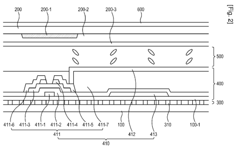
[16] FIG. 2 is a cross-section view of a display panel of FIG. 1;
[17] FIG. 3 is a view showing a color filter polarizing layer of FIG. 1;
[18] FIGs. 4a and 4b are views showing a metal linear grid of a sub pixel;
[19] FIG. 5 is a cross-section view of a color filter polarizing layer of
FIG. 3;
[20] FIG. 6 is a cross-section view of another color filter polarizing
layer according to an
exemplary embodiment;
[21] FIG. 7 is a cross-section view of still another color filter
polarizing layer according to
an exemplary embodiment;
[22] FIGs. 8a to 8e are views for explaining a manufacturing method for a
display panel
CA 02826915 2013-08-08
3
WO 2012/111915 PCT/KR2012/000159
according to an exemplary embodiment;
[23] FIG. 9 is a view showing a layer structure of a display panel
according to another
exemplary embodiment;
[24] FIG. 10 is a cross-section view of the display panel of FIG. 9;
[25] FIG. 11 is a view showing a layer structure of a display panel
according to still
another exemplary embodiment;
[26] FIG. 12 is a cross-section of the display panel of FIG. 11;
[27] FIG. 13 is a schematic view of a display apparatus according to an
exemplary em-
bodiment;
[28] FIG. 14 is a control block diagram of a display apparatus according to
an exemplary
embodiment; and
[29] FIG. 15 is a view for explaining a manufacturing method of the display
apparatus of
FIG. 13.
Best Mode for Carrying out the Invention
[30] Below, exemplary embodiments will be described in detail with
reference to ac-
companying drawings so as to be easily realized by a person having ordinary
knowledge in the art. The exemplary embodiments may be embodied in various
forms
without being limited to the exemplary embodiments set forth herein.
Descriptions of
well-known parts are omitted for clarity, and like reference numerals refer to
like
elements throughout.
[31] FIG. 1 shows a layer structure of a display panel according to an
exemplary em-
bodiment, and FIG. 2 is a cross-section view showing a display panel of FIG.
1.
[32] As shown therein, a display panel 1000 in this exemplary embodiment
includes first
and second substrates 100 and 200 opposite to each other, and a color filter
polarizing
layer 300, a pixel layer 400 and a liquid crystal layer 500 arranged in
sequence
between the first and second substrates 100 and 200, and a polarizing film 600
arranged on an outside surface of the second substrate 200. The display panel
1000
including the liquid crystal layer 500 may be used in a television, home
appliances
such as a monitor, a cellular phone, a portable multimedia player (PMP), a
Netbook, a
notebook computer, a mobile terminal such as an E-book terminal or the like, a
display
apparatus for exhibition and advertisement, etc.
[33] The color filter polarizing layer 300 and the pixel layer 400 are
formed in sequence
on the first substrate 100, and a polarizing film 600 is formed on the second
substrate
200. As shown in FIG. 2, the second substrate 200 is formed with a black
matrix 200-1
in a region corresponding to the TFT 411 of the first substrate 100, and a
common
electrode 200-3 generating a voltage corresponding to the pixel electrode 412.
The
liquid crystal layer 500, of which alignment is adjusted by applying a
voltage, is
CA 02826915 2013-08-08
4
WO 2012/111915 PCT/KR2012/000159
inserted between the first and second substrates 100 and 200. The array of the
liquid
crystal layer 500 is controlled in accordance with a twisted nematic (TN)
mode, a
vertical alignment (VA) mode, a patterned vertical alignment (PVA) mode, an in-
plane
switching (IPS) mode or the like operating mode of the display panel 1000. To
improve an optical viewing angle of the display panel 1000, sub pixels are
divided or
patterned, the refractive index of the liquid crystal is uniformly adjusted,
or the like
technology may be used.
[34] The color filter polarizing layer 300 is formed on the first substrate
100, and the pixel
layer 400 for controlling the liquid crystal array and displaying an image is
formed on
the color filter polarizing layer 300. The color filter polarizing layer 300
includes the
metal linear grid 310 arranged with different pitches so that first polarized
component
of the incident light can be emitted as light of different color. The
polarizing film 600
transmits light of a second polarized component different from the first
polarized
component. On the metal linear grid 310, a planarization layer 100-1 is formed
for
protecting and leveling the metal linear grid 310. The metal linear grid 310
included in
the color filter polarizing layer 300 will be described below in detail.
[35] The pixel layer 400 formed on the planarization layer 100-1 includes a
plurality of
pixels (not shown) for changing the liquid crystal array filled in the liquid
crystal layer
500 on the basis of a control signal received from the exterior, and each
pixel includes
a plurality of sub pixels 410. In this exemplary embodiment, the sub pixels
410
represent the smallest unit pixels in which video signal values corresponding
to red,
green and blue are input, and a unit, which includes a plurality of sub pixels
410 and
expresses one video signal, is regarded as the pixel. The sub pixel 410
includes a thin
film transistor (TFT) 411 as a switching device, and a pixel electrode 412.
The sub
pixel 410 has a two-dimensional spatial concept as well as a physical concept
including the TFT 411 and the pixel electrode 412.
[36] On the planarization layer 100-1 of the first substrate 100, the gate
electrode 411-1 is
formed. The gate electrode 411-1 may be a single or multiple layers containing
metal.
On the same layer as the gate electrode 411-1, there are further formed a gate
line (not
shown) connected to the gate electrode 411-1 and arranged in a transverse
direction of
the display panel 1000, and a gate pad (not shown) connected to a gate driver
(not
shown) and transmitting a driving signal to the gate line. Also, on the same
layer as the
gate electrode 411-1, a sustain electrode 413 is formed for building electric
charges up.
[37] On the first substrate 100, a gate insulating layer 411-2 containing
silicon nitride
(SiNx) or the like covers the gate electrode 411-1 and the sustain electrode
413.
[38] On the gate insulating layer 411-2 of the gate electrode 411-1, a
semiconductor layer
411-3 containing amorphous silicon or the like semiconductor is formed. On the
semi-
conductor layer 411-3, an ohmic contact layer 411-4 containing n+ hydrogenated
CA 02826915 2013-08-08
5
WO 2012/111915 PCT/KR2012/000159
amorphous silicon or the like material highly doped with silicide or n-type
impurities is
formed. Further, the ohmic contact layer 411-4 is removed in a channel portion
between a source electrode 411-5 and a drain electrode 411-6 to be described
later.
[39] On the ohmic contact layer 411-4 and the gate insulating layer 411-2,
data wiring
lines 411-5 and 411-6 are formed. The data wiring lines 411-5 and 411-6 may
also be a
single or multiple layer containing metal. The data wiring lines 411-5 and 411-
6
includes a data line (not shown) formed in a vertical direction and
intersecting a gate
line (not shown) to form the sub pixel 410, a source electrode 411-5 branched
from the
data line and extended to an upper portion of the ohmic contact layer 411-4,
and a
drain electrode 411-6 separated from the source electrode 411-5 and formed on
an
upper portion of the ohmic contact layer 411-4 opposite to the source
electrode 411-5.
[40] On the data wiring lines 411-5 and 411-6 and the semiconductor layer
411-3 that is
not covered with the data wiring lines 411-5 and 411-6, a passivation layer
411-7 is
formed. At this time, silicon nitride or the like inorganic insulting film may
be further
formed between the passivation layer 411-7 and the TFT 411, thereby securing
the re-
liability of the TFT 411.
[41] Typically, the pixel electrode 412 formed on the passivation layer 411-
7 contains
indium tin oxide (ITO) or indium zinc oxide (IZO), or the like transparent
conductive
material. The pixel electrode 412 is electrically connected to the source
electrode
411-5.
[42] On the planarization layer 100-1 of the second substrate 200, the
black matrix 200-1
is formed in a region corresponding to the TFT 411 of the first substrate 100.
Generally, the black matrix 200-1 serves to divide the sub pixels 410 and
prevent the
TFT 411 from being exposed to external light. The black matrix 200-1 contains
a pho-
tosensitive organic material with black dye. As the black dye, carbon black,
titanium
oxide or the like is used.
[43] On the black matrix 200-1, an overcoat layer 200-2 is formed for
leveling and
protecting the black matrix 200-1. As the overcoat layer 200-2, an acrylic
epoxy
material is typically used.
[44] On the overcoat layer 200-2, a common electrode 200-3 is formed. The
common
electrode 200-3 is made of a transparent conductive material such as indium
tin oxide
(ITO), indium zinc oxide (IZO), etc. The common electrode 200-3, together with
the
pixel electrode 412 of the first substrate 100, directly apply a voltage to
the liquid
crystal layer 500.
[45] FIG. 3 is a view showing a color filter polarizing layer of FIG. 1.
FIGs. 4a and 4b are
views for explaining a metal linear grid of a sub pixel, and FIG. 5 is a cross-
section
view of a color filter polarizing layer of FIG. 3.
[46] As shown therein, the metal linear grid 310 is shaped like a bar
arranged in certain
CA 02826915 2013-08-08
6
WO 2012/111915 PCT/KR2012/000159
direction on the first substrate 100. The metal linear grid 310 is
periodically arranged
with a certain height (H) and width (W). The cycle, i.e., the pitch of the
metal linear
grid 310 is controlled differently according to desired colors of light.
[47] If a pitch of a diffraction grid is adjusted to be equal to or shorter
than 1/2 of the
wavelength of the light, a diffraction wave is not formed but only transmitted
light and
reflected light exist. As shown therein, when the incident light passes
through the
metal linear grid 310 shaped like a slit, the first polarized component of the
incident
light, which is perpendicular to the metal linear grid 310, is transmitted
through the
first substrate 100, but a second polarized component, which is perpendicular
to the
metal linear grid 310, becomes reflected light which is reflected once again.
That is,
the incident light passing through the color filter polarizing layer 300 is
polarized with
respect to a certain direction. Meanwhile, air may be formed in between the
metal
linear grids 310.
[48] FIG. 4a is a view showing a pixel I and sub pixels 410-R, 410-G and
410-B con-
stituting the pixel I. In this exemplary embodiment, the pixel I includes a
red sub pixel
410-R formed in a region where red light is emitted, a green sub pixel 410-G
formed in
a region where green light is emitted, and a blue sub pixel 410-B formed in a
region
where blue light is emitted. The color filter polarizing layer 300
corresponding to such
a pixel layer 400 is formed with the metal linear grid 310 having different
pitches
according to the sub pixels 410-R, 410-G and 410-B.
[49] FIG. 4b is a view showing the metal linear grid 310 corresponding to
the sub pixels
410-R, 410-G and 410-B. The metal linear grid 310 includes a red metal linear
grid
310-R formed in a region corresponding to the red sub pixel 410-R, a green
metal
linear grid 310-G formed in a region corresponding to the green sub pixel 410-
G, and a
blue metal linear grid 310-B formed in a region corresponding to the blue sub
pixel
410-B.
[50] The red metal linear grid 310-R is arranged such that every pitch is
shorter than 1/2
of a red light wavelength, the green metal linear grid 310-G is arranged such
that every
pitch is shorter than 1/2 of a green light wavelength, and the blue metal
linear grid
310-B is arranged such that every pitch is shorter than 1/2 of a blue light
wavelength.
Thus, each pitch of the metal linear grids 310-R, 310-G and 310-B is adjusted
in ac-
cordance with the sub pixels 410-R, 410-G and 410-B, so that the wavelength of
the
incident light can be controlled to thereby allow the sub pixels 410 to emit
light of
different colors, respectively.
[51] The pitch of the red metal linear grid 310-R is shorter than 1/2 of
the red light
wavelength, i.e., about 330 ¨ 390nm, and the incident light is separated into
a red light
spectrum having a first polarized component while passing through the red
metal linear
grid 310-R. The pitch of the green metal linear grid 310-G is shorter than 1/2
of the
CA 02826915 2013-08-08
7
WO 2012/111915 PCT/KR2012/000159
green light wavelength, i.e., about 250 - 290nm, and the incident light is
separated into
a green light spectrum having the first polarized component. The pitch of the
blue
metal linear grid 310-B may be set up to be shorter than 1/2 of the blue light
wavelength, i.e., about 220 - 240nm. The light passing through the blue metal
linear
grid 310-B is separated into a blue light spectrum having the first polarized
component.
In other words, the pitches of the metal linear grid 310 are decreased in
order of the red
metal linear grid 310-R, the green metal linear grid 310-G and the blue metal
linear
grid 310-B. The pitch of the metal linear grid 310 may be adjusted in
accordance with
light wavelengths of color desired to be emitted from the display panel 1000,
and light
of yellow, cyan and magenta may be emitted instead of the foregoing light of
red,
green and blue.
11521 As shown in FIG. 5, the metal linear grid 310 in this exemplary
embodiment includes
a first metal layer 311, an insulating layer 313 and a second metal layer 315
stacked in
sequence. The first metal layer 311 and the second metal layer 315 may be made
of
metal such as Al, Ag, etc. and may have a height of less than about 100nm. In
this
exemplary embodiment, each of the first metal layer 311 and the second metal
layer
315 may be formed to have a height of about 40nm. The insulating layer 313
stacked
between the first metal layer 311 and the second metal layer 315 may include a
di-
electric material such as ZnSe and Ti02, and may be formed to have a height of
less
than about 150nm. The height of the metal linear grid 310 is larger than the
width
thereof, and a ratio of height to width may be 2 - 4, for example, 3. In the
metal linear
grid 310, the width, the height, the pitch, the ratio of height to width, and
a ratio of
pitch to width may be varied depending on the material forming the metal
linear grid
310. That is, simulation about optical transmittance is conducted by taking
the kind of
metal, the height of dielectric material, etc. into account, and an optimal
condition may
be selected. Also, the width, the height, the pitch, the ratio of height to
width, and a
ratio of pitch to width of the metal linear grid 310 may be varied depending
on color of
emitted light, i.e., each sub pixel 410.
11531 The principle that colored light is emitted from the metal layer 311,
315 of the metal
linear grid 310 is based on Plasmon that free electrons in metal are
collectively os-
cillated. Nano-sized metal shows Plasmon resonance on a surface of the metal
due to
the oscillation of the free electrons. The surface Plasmon resonance is
collective charge
density oscillation of the electrons on the surface of a metal thin film, and
a surface
Plasmon wave caused by the surface Plasmon resonance is a surface
electromagnetic
wave propagating along a boundary surface between the metal and the dielectric
material adjacent to the metal. As a kind of surface electromagnetic wave
propagating
along the boundary surface between metal and the dielectric material, the
surface
Plasmon wave corresponds to a wave generated when light incident to the metal
CA 02826915 2013-08-08
8
WO 2012/111915 PCT/KR2012/000159
surface and having a certain wavelength is not totally reflected and causes a
surface
wave. If the metal linear grid 310 including the first metal layer 311, the
insulating
layer 313 and the second metal layer 315 is arranged in the form of slits in a
certain
cycle, the color of emitted light is varied depending on the cycle.
11541 According to this exemplary embodiment, the metal linear grid 310 is
configured to
make white light filter into individual colors throughout a visible light
region. This is
to achieve a nano oscillator for quantum-Plasmon-quantum conversion within a
certain
oscillation wavelength, which enhances a pass bandwidth and makes compactness
possible as compared with other color filtering methods. Also, the filtered
light has
already been naturally polarized, so that it can be directly applied to an LCD
panel or
the like without any separate polarizing layer.
11551 Accordingly, the display panel 100 can generate polarized colored
light through one
color filter polarizing layer 300 instead of the existing polarizing film and
color filter.
Also, light that is not transmitted through the first substrate 100 is not
absorbed but is
instead reflected from the first metal layer 311 of the metal linear grid 310,
making it
likely to be reflected again toward the display panel 1000. That is, the total
optical ef-
ficiency is improved so that the conventional dual brightness enhance film
(DBEF) can
be omitted.
11561 If light enters through the bottom of the first substrate 100 and
exits through the
second substrate 200, the light of only the first polarized component enters
the liquid
crystal layer 500, and the light of the second polarized component is
reflected from the
first substrate 100. Typically, a backlight assembly (not shown) emitting
light under
the display panel 1000 includes a reflective plate that reflects light
reflected from the
first substrate 100 toward the display panel 1000 again. Metal contained in
the metal
linear grid 310 may have high reflectivity so that more much light can be
recycled by
the reflective plate and enter the first substrate 100, i.e., more much light
of the second
polarized component can enter the reflective plate. For example, the metal
linear grid
310 may include metal having high reflectivity, such as Al, Ag, Cu, etc. Thus,
if the
highly-reflective metal causes the reflectivity of the metal linear grid 310,
it is possible
to omit the dual brightness enhance film (DBEF) used in the conventional
display
panel. Accordingly, there is an effect on reducing production costs of the
display panel
1000, and it is possible to make the display apparatus including the display
panel 1000
thin and lightweight.
11571 FIG. 6 is a cross-section view of another color filter polarizing
layer according to an
exemplary embodiment.
11581 As shown therein, the color filter polarizing layer 300 may further
include a di-
electric layer 320 formed under the metal linear grid 310. The dielectric
layer 320 may
be made of a material similar to the first substrate 100, and may contain
MgF2. The di-
CA 02826915 2013-08-08
9
WO 2012/111915 PCT/KR2012/000159
electric layer 320 may be provided in the form of a film coupled to the first
substrate
100. Here, the dielectric layer 320 may replace the first substrate 100 or may
be
omitted.
[59] FIG. 7 is a cross-section view of still another color filter
polarizing layer according to
an exemplary embodiment.
[60] As shown therein, the display panel 1000 may further include a light
absorbing layer
330 formed on the metal linear grid 310 included in the first substrate 100
and
absorbing light. If external light enters the display panel 1000 and is
reflected again,
there are problems that a contrast ratio of the display panel 1000 may be
lowered and
picture quality may be deteriorated due to the reflection of light. To prevent
these
problems, the first substrate 100 according to this exemplary embodiment
includes the
light absorbing layer 330 on the metal linear grid 310 in order to absorb
undesired
external light.
[61] The light absorbing layer 330 may contain metal having low
reflectivity, and or may
include or be configured with carbon, chrome oxide, etc. for absorbing the
light.
[62] Alternatively, the light absorbing layer 330 may be formed not on the
first substrate
100 but beneath the second substrate 200. That is, the external light is
intercepted by
the light absorbing layer and thus prevented from entering the display panel
1000.
[63] FIGs. 8a to 8e are views for explaining a manufacturing method for a
display panel
according to an exemplary embodiment.
[64] As shown in FIG. 8a, the first metal layer 311, the insulating layer
313 and the
second metal layer 315 are stacked in sequence by a sputtering method or the
like in
order to form a color filter polarizing layer 300 on the first substrate 100.
[65] Then, as shown in FIG. 8b, a general patterning process is performed.
In other words,
photoresist is deposited, exposed to light through a mask, and developed and
etched to
thereby form the metal linear grid 310. That is, the first metal layer 311,
the insulating
layer 313 and the second metal layer 315 are not respectively formed but
stacked in
sequence and once patterned to form the metal linear grid 310. The process of
forming
the metal linear grid 310 may be achieved by any publicly-known or not-known
patterning technique.
[66] After forming the metal linear grid 310, as shown in FIG. 8c, the
planarization layer
100-1 is formed for protecting and leveling the surface of the metal linear
grid 310.
The planarization layer 100-1 may contain silicon nitride SiNx.
[67] Then, as shown in FIG. 8d, the TFT 411 and the pixel electrode 412
electrically
connected to the TFT 411 are formed on the planarization layer 100-1. The
pixel
electrode 412 may be formed by depositing metal by the sputtering method and
patterning it.
[68] FIG. 8e is views for explaining a manufacturing method for the second
substrate 200.
CA 02826915 2013-08-08
10
WO 2012/111915 PCT/KR2012/000159
As shown, the black matrix 200-1 is formed on the second substrate 200 in a
region
corresponding to the TFT 411, and the overcoat layer 200-2 is formed for
leveling the
black matrix 200-1. Further, the common electrode 200-3 containing a
transparent
conductive material is formed by a sputtering method.
[69] Thereafter, if FIGs. 8D and 8E are coupled and then the polarizing
film 600 is
attached to an outside surface of the second substrate 200, the display panel
1000 is
completed as shown in FIG. 2.
[70] FIG. 9 is a view showing a layer structure of a display panel
according to another
exemplary embodiment, and FIG. 10 is a cross-section view of the display panel
of
FIG. 9.
[71] As shown therein, the display panel 1000 according to this exemplary
embodiment
includes a polarizing film 600 formed on the outer surface of the firs
substrate 100, and
a color filter polarizing layer 300 formed on the second substrate 200. In
other words,
the color filter polarizing layer 300 may be arranged on not the pixel layer
400 but on
the substrate formed with the black matrix 200-1. If light enters through the
bottom of
the first substrate 100, the light of second polarized component passed
through the po-
larizing film 600 passes through the liquid crystal layer 500, and then emits
as the light
of the first polarized component with different colors while passing through
the color
filter polarizing layer 300. Each of the color filter polarizing layer 300 and
the po-
larizing film 600 may be selectively formed on the same or different
substrates as the
pixel electrode 400. Of course, light may enter though the second substrate
200 and
exit through the first substrate 100.
[72] In this exemplary embodiment, because the metal linear grid 310 is
formed on the
second substrate 200 through which the light exits, the metal linear grid 310
may
contain metal having low reflectivity so as to suppress reflection of external
light and
absorb the light. The metal linear grid 310 may undergo additional processes
for de-
creasing the reflectivity of the metal, or may include or be configured with
carbon,
chrome oxide, etc. for absorbing the light.
[73] In the meantime, the metal linear grid 310 according to another
exemplary em-
bodiment may include metal having high strength in consideration of external
impacts.
For example, the second metal linear grid 610 may contain MoW or the like
alloy, or
may contain conductive polymer capable of performing substantially the same
function
as the metal layer.
[74] FIG. 11 is a view showing a layer structure of a display panel
according to still
another exemplary embodiment, and FIG. 12 is a cross-section of the display
panel of
FIG. 11.
[75] As shown therein, the display panel 1000 in this exemplary embodiment
further
includes an additional polarizing layer 700 beneath the color filter
polarizing layer 300
CA 02826915 2013-08-08
11
WO 2012/111915 PCT/KR2012/000159
to transmit the first polarized component. The additional polarizing layer 700
may
include an additional metal linear grid 710 that contains substantially the
same metal as
metal contained in the metal linear grid 310 and is arranged in the same
direction as the
metal linear grid 310. The additional metal linear grid 710 is arranged in the
same
direction as the metal linear grid 310, and thus transmits the first polarized
component.
The light of the first polarized component passed through the additional
polarizing
layer 700 is emitted with red, blue and green colors while passing through the
color
filter polarizing layer 300.
[76] The metal layer contained in the additional metal linear grid 710 may
contain highly-
reflective metal, e.g., at least one of Al, Ag and Cu. Further, a light
absorbing layer
may be further provided on the metal layer and absorb external light.
[77] The display panel 1000 may further include a printed circuit board
mounted with a
gate driving integrated chip (IC) and a data chip film package although they
are not
shown. Also, a compensation film (not shown) may be further provided outside
the
first substrate 100 and the second substrate 200.
[78] FIG. 13 is a schematic view of a display apparatus according to an
exemplary em-
bodiment, and FIG. 14 is a control block diagram of a display apparatus
according to
an exemplary embodiment.
[79] As shown therein, the display apparatus 1 includes the display panel
1000, the
backlight assembly 2000, accommodating containers 3100, 3200, 3300 accom-
modating the display panel 1000 and the backlight assembly 2000, and a video
provider 4000.
[80] The display panel 1000 includes the first substrate 100, the second
substrate 200
opposite to the first substrate 100, the liquid crystal layer (not shown)
interposed
between the first substrate 100 and the second substrate 200, and a panel
driver 800 for
driving the pixel layer 400 to display a video signal. The panel driver 800
may include
a gate driving IC 810, a data chip film package 820, and a printed circuit
board 830.
[81] The first substrate 100 and the second substrate 200 may be formed
with the pixel
layer 400, the color filter polarizing layer 300, the polarizing film 600, the
black matrix
200-1, the common electrode 200-3, etc. The color filter polarizing layer 300
polarizes
the incident light entering the first substrate 100, and the polarizing film
600 polarizes
light exiting through the display panel 1000.
[82] The display panel 1000 receives external light and controls intensity
of light passing
through the liquid crystal layer interposed between the first substrate 100
and the
second substrate 200, thereby displaying an image.
[83] The gate driving IC 810 is integrated and formed on the first
substrate 100, and
connected to each gate line (not shown) formed on the first substrate 100.
Further, the
data chip film package 820 may be connected to each data line (not shown)
formed on
CA 02826915 2013-08-08
12
WO 2012/111915 PCT/KR2012/000159
the first substrate 100. Here, the data chip film package 820 may include a
tape
automated bonding (TAB) tape where a semiconductor chip is adhered to a wiring
pattern formed on a base film by TAB technology. As an example of the chip
film
package, a tape carrier package (TCP), a chip on film (COF), etc. may be used.
[84] Meanwhile, the printed circuit board 830 may be mounted with driving
components
for inputting a gate driving signal to a gate driving IC 931 and for inputting
a data
driving signal to a data chip film package 820.
[85] The backlight assembly 2000 may include a light guide plate 2200 for
guiding light,
first and second light sources 2300a and 2300b for emitting light, a
reflective sheet
2400 placed beneath the light guide plate 2200, and one or more optical sheets
2100.
[86] The light guide plate 2200 serves to guide the light to be supplied to
the display panel
1000. The light guide plate 2200 may be made of transparent plastic panel such
as
acryl, and guide light emitted from the first and second light sources 2300a
and 2300b
to travel toward the display panel 1000 formed on the light guide plate 2000.
On the
rear of the light guide plate 2200, there may be various patterns for changing
a
traveling direction of the light entering the inside of the light guide plate
2200 toward
the display panel 1000.
[87] As shown in the drawing, the first light source 2300a and the second
light source
2300b may include a light emitting diode (LED) as a point light source. The
light
source is not limited to the LED, and may include a line light source such as
a cold
cathode fluorescent lamp (CCFL) or a hot fluorescent lamp (HCFL). The first
light
source 2300a and the second light source 2300b are electrically connected with
an
inverter (not shown) supplying power, and receive the power.
[88] The reflective sheet 2400 is provided under the light guide plate 2200
and reflects the
light emitted under the light guide plate 2200 upward. Specifically, the
light, which is
not reflected by a fine dot pattern formed on the back of the light guide
plate 2200, is
reflected again toward the light guide plate 2200, thereby decreasing loss in
the light
entering the display panel 1000 and enhancing uniformity of light transmitting
through
the exit surface of the light guide plate 2200.
[89] One or more optical sheets 2100 are provided on the top of the light
guide plate 2200
and serve to diffuse and condense the light transmitted from the light guide
plate 2200.
The optical sheets 2100 may further include a diffusion sheet, a prism sheet,
a
protection sheet, etc. The diffusion sheet may be placed between the light
guide plate
2200 and the prism sheet, and diffuses incident light from the light guide
plate 2200 to
thereby prevent the light from being partially concentrated. The prism sheet
may
include triangular prisms regularly arranged on the top thereof, and serve to
condense
the light diffused by the diffusion sheet in a direction perpendicular to the
display
panel 1000. The protection sheet may be formed on the prism sheet, to protect
the
CA 02826915 2013-08-08
13
WO 2012/111915 PCT/KR2012/000159
surface of the prism sheet, and diffuse the light and thus uniformly
distribute the light.
[90] The accommodating container may include a lower accommodating
container 3100,
a middle accommodating container 3200 and an upper accommodating container
3300.
The lower accommodating container 3100 may accommodate the reflective sheet
2400, the first and second light sources 2300a and 2300b, the light guide
plate 2200,
and one or more optical sheets 2100. The lower accommodating container 3100
may
be made of metal having a strength capable of withstanding an external shock
and
ground ability.
[91] The video provider 4000 connects with the display panel 1000 and
provides a video
signal. Although not shown in FIG. 13, the video provider 4000 may be arranged
on
the reflective sheet 2400 and the lower accommodating container 3100, or may
be
placed on the rear of the lower accommodating container 3100.
[92] FIG. 15 is a view for explaining a manufacturing method of the display
apparatus of
FIG. 13.
[93] First, at operation S10, the color filter polarizing layer 300
including the metal linear
grid 310 arranged at different pitches to make the first polarized component
of the light
exit the display apparatus with different colors are formed on the first
substrate 100. At
this time, the metal linear grid 310 may include the red metal linear grid
arranged such
that every pitch is shorter than 1/2 of a red light wavelength, the green
metal linear grid
arranged such that every pitch is shorter than 1/2 of a green light
wavelength, and the
blue metal linear grid arranged such that every pitch is shorter than 1/2 of a
blue light
wavelength. Of course, the metal linear grid may be arranged or formed with
pitches
different from the above in accordance with the colors of the light. The metal
linear
grid 310 may be formed by stacking the first metal layer 311, the insulating
layer 313
and the second metal layer 315 in sequence and applying the sputtering process
thereto.
[94] Beneath the metal linear grid 310 may be provided the dielectric layer
320, and on
the metal linear grid 310 may be provided the light absorbing layer 330 for
suppressing
reflection of light.
[95] Characteristics of metal forming the metal linear grid 310, i.e.,
reflectivity or strength
of the metal may be varied depending on whether the metal linear grid 310 is
formed
on the substrate for incident light or on the substrate for exiting light.
[96] On the color filter polarizing layer 300, the pixel layer 400
including the plurality of
sub pixels 410 is formed at operation S20. Alternatively, the pixel layer 400
may be
formed on the substrate different from the color filter polarizing layer 300,
i.e., the
second substrate 200.
[97] On the second substrate 200 having no pixel layer 400, the black
matrix 200-1, the
overcoat layer 200-2 and the common electrode 200-3 are formed.
CA 02826915 2013-08-08
14
WO 2012/111915 PCT/KR2012/000159
[98] Then, at operation S30, the first substrate 100 and the second
substrate 200 are en-
capsulated, and the liquid crystal is injected between the first substrate 100
and the
second substrate 200.
[99] At operation S40, the polarizing film 600 is attached to the outer
surface of the
second substrate 200 having no color filter polarizing layer 300, thereby
transmitting
the second polarized component of light different from the first polarized
component.
With this process, the display panel 1000 is completed.
[100] Next, the video provider 4000 capable of supplying video data to the
sub pixels 410
and the panel driver 800 for driving the pixel layer 400 are connected to the
substrate,
and assembled to the backlight assembly 2000 including the light sources 2300a
and
2300b, thereby completing the display apparatus 1 as shown in FIG. 13.
[101] As described above, according to an exemplary embodiment, there are
provided a
display panel and a display apparatus comprising the same, in which
manufacturing
costs are decreased and a manufacturing process is simplified.
[102] According to another exemplary embodiment, there are provided a
display panel
having improved optical efficiency and a display apparatus comprising the
same.
[103] Although a few exemplary embodiments have been shown and described,
it will be
appreciated by those skilled in the art that changes may be made in these
exemplary
embodiments without departing from the principles and spirit of the inventive
concept,
the scope of which is defined in the appended claims and their equivalents.
CA 02826915 2013-08-08