Note: Descriptions are shown in the official language in which they were submitted.
CA 02827028 2013-08-12
OPTICAL FREQUENCY SHIFTER AND OPTICAL MODULATOR USING THE SAME
Technical Field
[0001]
The present invention relates to an optical frequency
shifter and an optical modulator using the same, and more
particularly, to an optical frequency shifter that shifts input
continuous light into two optical frequencies, and an all-optical
frequency-division multiplexing optical modulator using the
same.
Background Art
[0002]
Due to vigorous communication demands, investigations
towards increasing the capacity of backbone networks are being
actively conducted. With increases in transmission capacity,
if wavelength-division multiplexing (WDM) is used together with
raising the per-wavelength symbol rate (the modulation symbol
delivery speed), the effects of wavelength dispersion and
polarization mode dispersion increase sharply. Furthermore,
the optical intensity for obtaining a required reception
sensitivity for transmission increases, and signal quality
degradation due to four-wave-mixing, cross-phase modulation,
self-phase modulation, and the like produced inside the optical
fiber also become problematic.
[0003]
- 1 -
CA 02827028 2013-08-09
In order to solve such problems, technology that uses
orthogonal frequency-division multiplexing (OFDM) on each
wavelength channel and multiplexes the above with WDM is being
investigated as a multiplexing technology with excellent
dispersion resistance and high bandwidth utilization efficiency.
With OFDM, by encoding N carriers (where N is an integer equal
to or greater than 2) orthogonal to each other, the symbol rate
can be lowered to 1 / N compared to the case of a single carrier,
and the dispersion resistance can be improved. OFDM is a
general-purpose technology in the field of radio.
[0004]
As a technology that OFDM modulates an optical signal,
there is a method that electrically generates an OFDM signal
similarly to radio and drives an optical modulator (see PTL 1) .
The optical system is simple if this technique is used, but since
the modulator and the modulator driving unit demand bands of
approximately N times the symbol rate, there is a problem in
that these bands become a limiting factor.
[0005]
Meanwhile, all-optical OFDM that multiplexes sub-carrier
light pre-modulated by an optical modulator has been proposed
(see PTL 2 and 3) . As illustrated in FIG. 1, first, multiple
sub-carrier light beams are generated with a multi-carrier
generation circuit (optical sub-carrier generator) 101. Next,
these sub-carrier light beams are discriminated into individual
sub-carrier light beams with an optical separation unit 102,
and after being respectively data-modulated by optical
- 2 -
CA 02827028 2015-07-22
orthogonal modulators 103a and 103b, are multiplexed by an
optical multiplexer 104 to obtain a modulated output. As
disclosed in PTL 3, the optical separation unit 102 may comprise
delayed interferometers 105, 106a, and 106b. In so doing, a
high extinction ratio can be obtained, even in the case where
the optical frequency grid of the WDM signals (the optical
frequency interval between WDM optical signals) and the
sub-carrier interval differ to some degree. Although FIG. 1
illustrates the case of two sub-carriers, the optical circuit
on the transmitting side is also comparatively simple in this
case, and thus is promising as a next-generation high-speed
transmission technology.
Citation List
Patent Literature
[0006]PTL 1: Japanese Patent Laid-Open No. 2005-311722
PTL 2: Japanese Patent Laid-Open No. 2009-017320
PTL 3: Japanese Patent Laid-Open No. 2009-198914
Summary
Technical Problem
[0007]
However, with the above configuration of the all-optical
OFDM modulator, it is necessary to use delayed interferometers
105 and 106 in the optical separation unit 102 for the purpose
of sub-carrier discrimination, and there is a problem in that
the circuit size becomes larger for this reason. In order to
- 3 -
CA 02827028 2013-08-09
set the frequency grid of the WDM to 100 GHz, it is necessary
to set the free spectrum range (FSR) of the delayed
interferometers to approximately 50 GHz (see PTL 3). If the
delayed interferometers are manufactured with a silica optical
waveguide (approximatelyN=1 . 49) , theopticalpathdifferential
of the delayed interferometers becomes approximately 4 mm. In
order to set the frequency interval of the wavelength channels
to the 50 GHz interval that is recently being adopted, the optical
path differential becomes double at approximately 8 mm, which
requires an optical separation unit with a large circuit size.
[0008]
Also, since the lithium niobate waveguides or silica
optical waveguides constituting the delayed interferometers
typically have an index of refraction that is
temperature-dependent, there is a problem in that the center
wavelength of the delayed interferometers changes according
to the environmental temperature . In order to resolve the above,
it is necessary to perform temperature adjustment or make the
delayed interferometers temperature-
independent.
Temperature adjustment complicates the implementation of the
modulator module, and also has the problem increasing power
consumption (typically several Watts). Temperature
independence has the problem of inducing increased loss
(typically around 1 dB).
[0009]
Furthermore, since it is necessary to set the FSR of the
delayed interferometers to match the optical frequency grid and
- 4 -
CA 02827028 2015-07-22
the sub-carrier interval, it is necessary to modify the design
of the delayed .interferometers for different frequency grids,
and there is a problem in that different optical separation units
become necessary.
[0010]
An aspect of the present disclosure being devised in light
of related technology like the above, takes as an object to provide
a temperature-independent optical frequency shifter that
generates sub-carriers with a miniaturizable configuration, as
well as to provide an all-optical OFDM modulator using the same
that is compact, has low temperature dependence, and is even
compatible with different frequency grids.
[0011]
In one aspect, the present disclosure provides an optical
frequency shifter comprising one input optical port; a 1-input,
2-output optical coupler optically connected to the one input
port; two Mach-Zehnder modulation units individually optically
connected to the two outputs of the 1-input, 2-output optical
coupler; a 2-input, 2-output optical coupler optically connected
to the individual outputs of the two Mach-Zehnder modulation
units; and two output optical ports optically connected to the
two outputs of the 2-input, 2-output optical coupler; wherein
the two Mach-Zehnder modulation units are driven by periodic
waveforms at the same frequency whose phases differ from each
- 5 -
CA 02827028 2015-07-22
other by (2p + 1) n / 2 (p: integer).
[0012]
The biases of the two Mach-Zehnder modulation units may
be adjusted such that the individual outputs become 0 when not
driven.
[0013]
The half-wave voltage of the Mach-Zehnder modulation units
may be Vn, the full voltage amplitude values of the periodic
waveforms that drive the Mach-Zehnder modulation units may be
within 60% to 120% inclusive of 2Vn.
[0014]
The 1-input, 2-output optical coupler may be a Y-optical
branch coupler, and the 2-input, 2-output optical coupler may
be a 2-input, 2-output multimode interference optical coupler.
[0015]
A first modulation electrode provided in a first one of
the two Mach-Zehnder modulation.units maybe cascade-connected
to a second modulation electrode provided in a second one of
the two Mach-Zender modulation units, and a delay of n / 2 in
the periodic waveform may be provided on an electrical line that
connects the first modulation electrode and the secondmodulation
electrode.
- 6 -
CA 02827028 2015-07-22
[0016]
The first modulation electrode may be shorter than the
second modulation electrode, and the first Mach-Zehnder
modulation unit may be closer to the electrical input than the
second Mach-Zehnder modulation unit.
[0017]
In another aspect, the present disclosure provides an
optical modulator that generates an optical signal, the optical
modulator comprising a 1-input, 2-output optical frequency
shifter unit; two optical modulation units individually
optically connected to the two outputs of the 1-input, 2-output
optical frequency shifter unit; and an optical multiplexing unit
optically connected to the individual outputs of the two optical
modulation units; wherein the 1-input, 2-output optical
frequency shifter unit is provided with one input optical port,
a 1-input, 2-output optical coupler optically connected to the
one input port, two Mach-Zehnder modulation units individually
optically connected to the two outputs of the 1-input, 2-output
optical coupler, a 2-input, 2-output optical coupler optically
connected to the individual outputs of the two Mach-Zehnder
modulation units, and two output optical ports optically
connected to the two outputs of the 2-input, 2-output optical
coupler, wherein the two Mach-Zehnder modulation units are driven
by periodic waveforms at the same frequency whose phases differ
from each other by (2p + 1) TC / 2 (p: integer) . =
- 7 -
CA 02827028 2015-07-22
[0018]
The two modulation units may be individual optical
orthogonal modulation units, and the optical multiplexing unit
may be a 2-input, 1-output optical coupler.
[0019]
The two modulation units may be individual polarization
multiplexing optical orthogonal modulation units, and the
optical multiplexing unit may be a 2-input, 1-output optical
coupler.
[0020]
The two modulation units maybe double optical orthogonal
modulation units individually optically connected to the two
outputs of an individual 1-input,2-output optical coupler and
a 1-input, 2-output optical coupler, the optical multiplexer
comprising a first 2-input, 1-output optical coupler that
multiplexes one output from each of the two double optical
orthogonal modulation units, a second 2-input, 1-output optical
coupler that multiplexes the other output from each of the two
double optical orthogonal modulation units, and a polarization
multiplexerthatpolarizationmultiplexestheoutputofthe first
optical coupler and the output of the second optical coupler,
and a polarization convertermaybe providedbetween one of either
the output of the first optical coupler and the output of the
second optical coupler, and the polarization multiplexer.
- 8 -
CA 02827028 2015-07-22
[0021]
The biases of the two Mach-Zehnder modulation units
provided in the optical frequency shifter may be adjusted such
that the individual outputs become 0 when not driven.
[0022]
The half-wave voltage of the Mach-Zehnder modulation
units provided in the optical frequency shifter may be Vn, the
full voltage amplitude values of the periodic waveforms that
drive the Mach-Zehnder modulation units provided in the optical
frequency shifter may be within 60% to 120% inclusive of 2Vn.
[00231
The 1-input, 2-output optical coupler provided in the
optical frequency shifter may be a Y-optical branch coupler,
and the 2-input, 2-output optical coupler provided in the optical
frequency shifter may be a 2-input, 2-output multimode
interference optical coupler.
[0024]
A first modulation electrode provided in a first one of
the two Mach-Zehnder modulation units provided in the optical
frequency shifter may be cascade-connected to a second
modulation electrode provided in a second one of the two
Mach-Zehnder modulation unit provided, and a delay of it / 2 in
the periodic waveform that drives the optical frequency shifter
may be provided on an electrical line that connects the first
- 9 -
CA 02827028 2015-07-22
modulation electrode and the second modulation electrode.
[0025]
The first modulation electrode may be shorter than the
second modulation electrode, and the first Mach-Zehnder
modulation unit may be closer to the electrical input than the
second Mach-Zehnder modulation unit.
Advantageous Effects
[0026]
By providing one input optical port; a 1-input, 2-output
optical coupler optically connected to the one input port; two
Mach-Zehnder modulation units individually optically connected
to the two outputs of the 1-input, 2-output optical coupler;
a 2-input, 2-output optical coupler optically connected to the
individual outputs of the two Mach-Zehnder modulation units;
and two output optical ports optically connected to the two
outputs of the 2-input, 2-output optical coupler; and by driving
the two Mach-Zehnder modulation units by periodic waveforms at
the same frequency whose phases differ from each other by it /
2, it is possible to provide an optical frequency shifter and
an optical modulator that do not require delayed
interferometers, are compact, do not have temperature dependency,
and do not depend on a wavelength grid.
- 10 -
CA 02827028 2015-07-22
Brief Description of Drawings
[0027]
[Fig. 1] Fig. 1 is a diagram illustrating a configuration
of an OFDM modulator of the related art;
[Fig. 2] Fig. 2 is a diagram illustrating a configuration
of an optical frequency shifter according to the first embodiment
of the present invention;
[Fig. 3] Fig. 3 is a diagram illustrating modulation
amplitude dependence of frequency shift components in an optical
- 11 -
CA 02827028 2013-08-09
frequency shifter according to the first embodiment of the
present invention;
[Fig. 4] Fig. 4 is a diagram illustrating frequency shift
components in an optical frequency shifter according to the first
embodiment of the present invention;
[Fig. 5] Fig. 5 is a diagram illustrating an output signal
obtained with an optical frequency shifter according to the first
embodiment of the present invention;
[Fig. 6] Fig. 6 is a diagram illustrating a configuration
of an optical frequency shifter according to a modification of
the first embodiment of the present invention;
[Fig. 7] Fig. 7 is a diagram illustrating a configuration
of an optical frequency shifter according to the second
embodiment of the present invention;
[Fig. 8] Fig. 8 is a diagram illustrating a simulation
of an output signal obtained with an optical frequency shifter
according to the second embodiment of the present invention;
[Fig. 9] Fig. 9 is a diagram illustrating a configuration
of an optical modulator according to the third embodiment of
the present invention;
[Fig. 10] Fig. 10 is a diagram illustrating a configuration
of an optical orthogonal modulation unit;
[Fig. 11] Fig. 11 is a diagram illustrating a configuration
of an optical modulator according to the fourth embodiment of
the present invention;
[Fig. 12] Fig. 12 is a diagram illustrating a configuration
of a polarization multiplexing optical orthogonal modulation
- 12 -
CA 02827028 2013-08-09
unit;
[Fig. 13] Fig. 13 is a diagram illustrating a configuration
of an optical modulator according to the fifth embodiment of
the present invention; and
[Fig. 14] Fig. 14 is a diagram illustrating a configuration
of an optical modulator according to a modification of the fifth
embodiment of the present invention.
Description of Embodiments
[0028]
Hereinafter, embodiments of the present invention will
be described with reference to the drawings and mathematical
formulas.
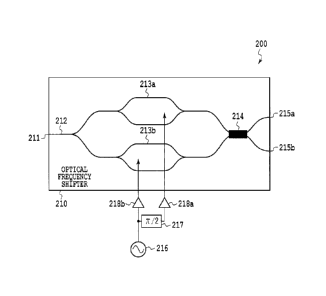
[0029] (First embodiment)
Fig. 2 illustrates a configuration of an optical frequency
shifter 210 according to the first embodiment of the present
invention. The optical frequency shifter 210 of the first
embodiment of the present invention comprises an input port 211,
a 1-input, 2-output optical coupler 212 optically connected to
the input port 211, two Mach-Zehnder modulation units
(hereinafter, HZ modulation units) 213a and 213b respectively
and optically connected to the two outputs of the optical coupler
212, a 2-input, 2-ouput optical coupler 214 individually and
optically connected to the two HZ modulation units 213a and 213b,
and output optical ports 215a and 215b individually and optically
connected to the two outputs of the 2-input, 2-output optical
coupler 214.
- 13 -
CA 02827028 2013-08-09
[0030]
The two HZ modulation units 213a and 213b are driven via
electrical amps 218a and 218b by electrical signals produced
by a signal generator 216, but as illustrated in Fig. 2, the
driving unit of the HZ modulation unit 213a is provided with
an electrical delay line 217 having a phase shift of 7 / 2. As
a result, the two HZ modulation units 213a and 213b become driven
by identical electrical waveforms whose phase differs by 7 /
2.
[0031]
Herein, in the optical frequency shifter 210 according
to the first embodiment of the present invention illustrated
in Fig. 2, a Y-optical branch coupler is used as the 1-input,
2-output optical coupler 212. This is because taking such a
configuration makes it possible to provide a 1-input, 2-output
optical coupler with a wide range of operating wavelengths and
small splitting ratio instability. However, the present
invention is not limited to this example, and for the 1-input,
2-output optical coupler, a 1-input, 2-output multimode
interference optical coupler may also be used, and additionally
a directional coupler, a 2-input, 2-output multimode
interference optical coupler, or one of the input ports of a
2-input, 2-output optical coupler such as an asymmetric X-
coupler may also be used.
[0032]
Also, in the optical frequency shifter 210 according to
the first embodiment of the present invention illustrated in
- 14 -
CA 02827028 2013-08-09
Fig. 2, a multimode interference optical coupler is used as the
2-input, 2-output optical coupler 214. This is because taking
such a configuration makes it possible to provide a 2-input,
2-output optical coupler with a wide range of operating
wavelengths. However, the present invention is not limited to
this example, and obviously the use of another coupler, such
as a directional coupler, an asymmetric X-coupler, or a wideband
optical coupler using a lattice configuration, is also
acceptable.
[0033]
Also, in the optical frequency shifter 210 according to
the first embodiment of the present invention illustrated in
Fig. 2, a Y-optical branch coupler with two in-phase optical
outputs is used as the 1-input, 2-output optical coupler 212,
and a multimode interference optical coupler that produces a
90 degree phase difference between two optical outputs is used
as the 2-input, 2-output optical coupler 214. This is not only
because a Y-optical branch coupler and a multimode interference
optical coupler are suitable as the respective couplers for the
first embodiment of the present invention, but also because
taking such a combination also has the merit of making it
unnecessary to insert an optical delay in the optical arm coupling
the Y-optical branch coupler 212 and the multimode interference
optical coupler 214. However, as illustrated in detail in a
modification of the first embodiment, the present invention is
not limited to this example.
[0034]
- 15 -
CA 02827028 2013-08-09
Next, operation of the optical frequency shifter 210
according to the first embodiment of the present invention will
be described. Herein, an input waveform into the optical
frequency shifter 210 is expressed as E = EO (t) . At this point,
since input light is guided by the Y-optical branch coupler 212
to the MZ modulation units 213a and 213b while keeping the same
phase, the input optical fields Fain (t) and Elgin (t) of the MZ
modulation units 213a and 213b are respectively expressed as
in Eq. 1 and Eq. 2 below.
[0035] [Math. 1]
1
Eam = __
Eq. 1
[0036] [Math. 2]
1
I n
E, (0=
42
= = = Eq. 2
[0037]
At this point, the driving waveform Db (t) of the MZ
modulation unit 213b is expressed as in Eq. 3 below, assuming
a sine wave for simplicity.
[0038] [Math. 3]
DI, (0= m sin (277f )
Eq. 3
[0039]
Herein, m is a proportionality coefficient, and f is the
frequency of the driving waveform. The driving waveform Da (t)
of the MZ modulation unit 213a receives a delay of 7C / 2 from
the electrical delay line 217, and thus becomes like Eq. 4 below.
- 16 -
CA 02827028 2013-08-09
[0040] [Math. 4]
1 \
Dcittnisin 2[ t __
41,
=== Eq. 4
[0041]
Now assume that the MZ modulation units 213a and 213b
are bias-adjusted so as to indicate a sinusoidal response to
the respective driving waveforms. At this point, the optical
field outputs Eaout(t) and Ebout(t) of the MZ modulation units
213a and 213b are respectively expressed as in Eq. 5 and Eq.
6 below.
[0042] [Math. 5]
Eauut (r) - Ein insin 271 t- , - E,_,V , (m )sin
(u+ 1)1 t
= = Eq. 5
[0043] [Math. 6]
1
E:ut(r =
) sin [ni sin(2 rift )]= ¨E y1
, (in )s n-(2n + 1)ftl
_n+
=== Eq. 6
[0044]
Herein, Jn is an nth order Bessel function of the first
kind. These two optical fields are multiplexed by the multimode
interference optical coupler 214. At this point, in the
multimode interference optical coupler 214, the combined light
is given a phase shift of ic / 2, and thus the optical fields
El(t) and E2(t) obtained from the output ports 215a and 215b
are respectively given as in Eq. 7 and Eq. 8 below.
[0045] [Math. 7]
- 17 -
CA 02827028 2013-08-09
I
E, EõY. 2i(m), sin 2 1 7(2ii + 1)1 r 1+ isin[27(2/7+1)1r],
= Eq. 7
[0046] [Math. 8]
1
E,(r) = EõF J,(m) sin 27(2n- 1)11 t __ + sin[277-(2ii +
;,="7 ' 4
= = = Eq. 8
[0047]
Expanding further, Eq. 9 and Eq. 10 below can be obtained.
[0048] [Math. 9]
Foil= ¨Eoy exp[ 1 2;r(2ii¨ 1))fr]
= = = Eq. 9
[0049] [Math. 10]
(r)= ¨jE1y.f1(m)(-1r exp[(--- 1)" 27r. (217 + 1)itt]
= = = Eq. 10
[0050]
Ignoring the higher-order terms and focusing on the n
= 0 term, El (t) and E2 (t) respectively become like Eq. 11 and
Eq. 12 below.
[0051] [Math. 11]
-E,Ji(m)exp(- ,j2rift)
= = Eq. 11
[0052] [Math. 12]
E (t) 0J1(111) exp(+ 277f r )
= Eq. 12
[0053]
Eq. 11 and Eq. 12 above demonstrate that El (t) is given
a frequency shift of -f from the original frequency, while E2 (t)
is given a frequency shift of +f from the original frequency.
- 18 -
CA 02827028 2013-08-09
[0054]
Herein, in the optical frequency shifter 210 according
to the first embodiment of the present invention illustrated
in Fig. 2, the driving waveform Da (t) of the HZ modulation unit
213a is taken to receive a delay of TE / 2 from the electrical
delay line 217, but obviously it is also acceptable to provide
the electrical delay line 217 on the side of the HZ modulation
unit 213b and apply the / 2 delay to the driving waveform Db (t) .
In this case, f indicated in the formulas is replaced with -f.
Furthermore, generally the advantageous effects of the present
invention can be exhibited if a phase difference of (2p + 1)
TE / 2 is applied between Da (t) and Db (t) , where p is an integer.
[0055]
Also, in the optical frequency shifter 210 according to
the first embodiment of the present invention illustrated in
Fig. 2, the driving waveforms Da (t) and Db (t) of the HZ modulation
units 213a and 213b are assumed to be sine waves, but this is
because the generation of such waveforms is easy, and furthermore
because the load on the driving electrical system can be reduced
since the waveform is narrow. However, the present invention
is not limited to this example, and obviously a waveform other
than a sine wave is also acceptable. In this case, the
coefficients applied to the Bessel functions in Eq. 9 and Eq.
will change.
[0056]
Fig. 3 is a diagram illustrating the relationship 300
between the driving amplitude m of an optical frequency shifter
- 19 -
CA 02827028 2013-08-12
,
,
according to the first embodiment of the present invention, and
the obtained optical frequency components. In the drawing, an
f component, a 3f component, and a 5f component are depicted.
Of these, the f component becomes important for the operation
of the optical frequency shifter, and the drawing demonstrates
that the f component is maximized when m = 1.17n. Meanwhile,
since there is an aspect of the load on the driving electrical
system increasing as the driving amplitude increases, a driving
amplitudem from 60% to 120% ofn is desirable . This is equivalent
to setting the full amplitude from 60% to 120% of 2Vn, provided
the half-wave voltage of an MZ modulation unit is Vn.
[0057]
Fig. 4 is a diagram illustrating the results 400 of
calculating the optical frequency spectrumobtained at the output
optical port 215b when driving an optical frequency shifter
according to the first embodiment of the present invention. The
horizontal axis represents the optical frequency normalized to
f, while the vertical axis is the optical power. Also, the
driving amplitude m is taken to be 1.17n. Eq. 10 demonstrates
that the optical frequency after passing through the optical
frequency shifter becomes +f, -3f, +5f, -7f, and so on.
[0058]
Fig. 5 is a diagram illustrating a waveform 500 obtained
when configuring an optical frequency shifter according to the
first embodiment of the present invention and actually driving.
Fig. 5 demonstrates that by using an optical frequency shifter
- 20 -
CA 02827028 2013-08-09
of the present invention, output whose optical frequency is
respectively shifted by -f and+f is obtained at the output optical
ports 215a and 215, respectively.
[0059]
With this configuration, optical delayed interferometers
for discriminating the f optical frequency components become
unnecessary, thus making it possible to provide an optical
frequency shifter of small size, in which it is unnecessary to
take into account changes in the characteristics of the delayed
interferometers due to temperature. In addition, since there
are no optical delayed interferometers, it is possible to provide
an optical frequency shifter that is not limited to operation
on a specific wavelength grid, but is capable of operating on
any frequency grid.
[0060] (Modification of first embodiment)
Fig. 6 illustrates a configuration of an optical frequency
shifter 610 according to a modification of the first embodiment
of the present invention. The optical frequency shifter 610
according to a modification of the first embodiment of the present
invention comprises an input port 611, a 1-input, 2-output
optical coupler 612 optically connected to the input port 611,
two Mach-Zehnder modulation units (hereinafter, MZ modulation
units) 613a and 613b individually and optically connected to
the two outputs of the optical coupler 612, a 2-input, 2-ouput
optical coupler 614 individually and optically connected to the
two MZ modulation units 613a and 613b, and output optical ports
615a and 615b individually and optically connected to the two
- 21 -
CA 02827028 2013-08-12
outputs of the 2-input, 2-output optical coupler 614.
[0061]
The two MZ modulation units 613a and 613b are driven via
electrical amps 618a and 618b by electrical signals produced
by a signal generator 616, but as illustrated in Fig. 6, the
driving unit of the MZ modulation unit 613b is provided with
an electrical delay line 617 having a phase shift of it / 2. As
a result, the two MZ modulation units 613a and 613b become driven
by identical electrical waveforms whose phase differs by it /
2. In the optical frequency shifter according to the first
embodiment of the present invention illustrated in Fig. 2, the
electrical delay line 217 is provided on the driving system of
the MZ modulation unit 213a, but obviously the advantageous
effects of the present invention can be exhibited even if the
electrical delay line 617 is provided for the driving unit of
theMZmodulationunit613b, as withthe optical frequencyshifter
610 according to a modification of the first embodiment of the
present invention illustrated in Fig. 6.
[0062]
Also, in the optical frequency shifter 610 according to
a modification of the first embodiment of the present invention
illustratedin Fig. 6, al-input, 2-outputmultimode interference
optical coupler is used as the 1-input, 2-output optical coupler
612. In the optical frequency shifter 210 according to the first
embodiment of the present invention illustrated in Fig. 2, a
Y-optical branch coupler is used as the 1-input, 2-output optical
coupler 212, but obviously the advantageous effects of the
- 22 -
CA 02827028 2013-08-12
present invention can be exhibited even if a 1-input, 2-output
multimode interference optical coupler is used as the 1-input,
2-output optical coupler 612, as with the optical frequency
shifter 610 according to a modification of the first embodiment
of the present invention illustrated in Fig. 6.
[0063]
Furthermore, in the optical frequency shifter 610
according to a modification of the first embodiment of the present
invention illustrated in Fig. 6, a 2-input, 2-output X-coupler
having outputs with different waveguide widths as illustrated
in Fig. 6 is used as the 2-input, 2-output optical coupler 614.
This is because an X-coupler that uses adiabatic mode evolution
has low-loss characteristics over a wide band, making it possible
to provide a wideband, low-loss optical frequency shifter. In
addition, since with an X-coupler the phases between the combined
light become 0 and 'it, a TE / 2 optical delay line 619 is inserted
between the MZ modulation unit 613b and the 2-input, 2-output
optical coupler 614 in order to compensate. In the optical
frequency shifter 210 according to the first embodiment of the
present invention illustrated in Fig. 2, a 2-input, 2-output
multimode interference optical coupler is used as the 2-input,
2-output optical coupler 214, but obviously the advantageous
effects of the present invention can be exhibited even if an
X-coupler is used as the 2-input, 2-output optical coupler 614,
and an optical delay line 619 is used to compensate for the phase,
as with the optical frequency shifter 610 according to a
modification of the first embodiment of the present invention
- 23 -
CA 02827028 2013-08-09
illustrated in Fig. 6.
[0064] (Second embodiment)
Fig. 7 illustrates a configuration of an optical frequency
shifter 710 according to the second embodiment of the present
invention. The optical frequency shifter 710 of the second
embodiment of the present invention comprises an input port 711,
a 1-input, 2-output optical coupler 712 optically connected to
the input port 711, two HZ modulation units 713a and 713b
individually and optically connected to the two outputs of the
optical coupler 712, a 2-input, 2-ouput optical coupler 714
individually and optically connected to the two HZ modulation
units 713a and 713b, and output optical ports 715a and 715b
individually and optically connected to the two outputs of the
2-input, 2-output optical coupler 714.
[0065]
Herein, in the optical frequency shifter 710 according
to the second embodiment of the present invention illustrated
in Fig. 7, two HZ modulation units 713a and 713b are provided.
The two HZ modulation units 713a and 713b are individually
equipped with modulation electrodes 720a and 720b. These
modulation electrodes 720a and 720b are connected by an
electrical line 721, with an electrical delay line 722 provided
between the modulation electrodes 720a and 720b such that an
electrical delay of Tr / 2 is applied between the driving waveforms
of the modulation electrodes 720a and 720b. In addition, the
electrical line 721 connecting the modulation electrodes 720a
and 720b is ultimately terminated by a terminating resistor 723.
- 24 -
CA 02827028 2013-08-09
The optical frequency shifter 710 is driven via an electrical
amp 718 by a driving waveform generated by a signal generator
716. With this configuration, one electrical amp is sufficient
to drive the M2 modulation units, making it possible to provide
an optical frequency shifter 710 with low power consumption.
[0066]
Herein, it is noted that although modulation electrodes
are obviously also provided in the HZ modulation units 213a,
613a and 213b, 613b included in the optical frequency shifter
210 according to the first embodiment of the present invention
and the optical frequency shifter 610 according to a modification
of the first embodiment of the present invention illustrated
in Fig. 2 and Fig. 6, modulation electrodes are omitted from
Fig. 2 and Fig. 6 which illustrate configurations.
[0067]
Inaddition, intheoptical frequencyshifter710 according
to the second embodiment of the present invention illustrated
in Fig. 7, the HZ modulation units 713a and 713b comprise x-cut
lithium niobate, and the modulation electrodes 720a and 720b
are single-electrode driving electrodes. However, the present
invention is not limited to this example, and the M2 modulation
units 713a and 713b may comprise z-cut lithium niobate and
polarization inversion, and the modulation electrodes 720a and
720bmaybe single-electrode driving electrodes . Alternatively,
the HZ modulation units 713a and 713b may comprise z-cut lithium
niobate, and the modulation electrodes 720a and 720b may be
dual-electrode driving electrodes. Obviously, HZ modulation
- 25 -
CA 02827028 2013-08-09
units 713a and 713b comprised of other types of materials are
also acceptable.
[0068]
Inaddition,intheopticalfrequencyshifter710according
to the second embodiment of the present invention illustrated
in Fig. 7, the length of the modulation electrode 720b closer
to the electrical input may be made shorter than the length of
the modulation electrode 720a farther from the electrical input
in order to account for loss on the electrical line from the
modulation electrode 720b to the modulation electrode 720a and
obtain the same degree of modulation with the MZ modulation units
713a and 713b. However, the present invention is not limited
to this example.
[0069]
Furthermore, in the optical frequency shifter 710
according to the second embodiment of the present invention
illustrated in Fig. 7, a Y-optical branch coupler is used as
the 1-input, 2-output optical coupler 712. This is because
taking such a configurationmakes it possible to provide a 1-input,
2-output optical coupler with a wide range of operating
wavelengths and a small splitting ratio instability. However,
the present invention is not limited to this example, and for
the 1-input, 2-output optical coupler, a 1-input, 2-output
multimode interference optical coupler may also be used, and
additionally a directional coupler, a 2-input, 2-output
multimode interference optical coupler, or one of the input ports
of a 2-input, 2-output optical coupler such as an asymmetric
- 26 -
CA 02827028 2013-08-09
X-coupler may also be used.
[0070]
Also, in the optical frequency shifter 710 according to
the second embodiment of the present invention illustrated in
Fig. 7, a multimode interference optical coupler is used as the
2-input, 2-output optical coupler 714. This is because taking
such a configuration makes it possible to provide a 2-input,
2-output optical coupler with a wide range of operating
wavelengths. However, the present invention is not limited to
this example, and obviously the use of another coupler, such
as a directional coupler, an asymmetric X-coupler, or a wideband
optical coupler using a lattice configuration, is also
acceptable.
[0071]
Fig. 8 is a diagram illustrating simulation values for
an optical spectrum obtained by an optical frequency shifter
according to the second embodiment of the present invention.
As illustrated in Fig. 8, two frequency-shifted optical outputs
can still be obtained with such a configuration.
[0072] (Third embodiment)
Fig. 9 illustrates a configuration of an optical modulator
900 according to the third embodiment of the present invention.
The optical modulator 900 according to the third embodiment of
the present invention illustrated in Fig. 9 comprises an optical
frequency shifter 910, optical orthogonal modulation units 924a
and 924b individually and optically connected to the two outputs
of the optical frequency shifter 910, and a 2-input, 1-output
- 27 -
CA 02827028 2013-08-09
optical coupler 925, optically connected to the outputs of the
optical orthogonal modulation units 924a and 924b, that
multiplexes the two outputs. Herein, an optical frequency
shifter according to the first embodiment of the present
invention is used as the optical frequency shifter 910.
[0073]
Herein, in the optical modulator 900 according to the
third embodiment of the present invention illustrated in Fig.
9, a Y-optical branch coupler is used as the 2-input, 1-output
optical coupler 925. This is because taking such a configuration
makes it possible to provide a 2-input, 1-output optical coupler
with a wide range of operating wavelengths and a small splitting
ratio instability. However, the present invention is not
limited to this example, and for the 2-input, 1-output optical
coupler, a 2-input, 1-output multimode interference optical
coupler may also be used, and additionally a directional coupler,
a 2-input, 2-output multimode interference optical coupler, or
one of the output ports of a 2-input, 2-output optical coupler
such as an asymmetric X-coupler may also be used.
[0074]
In addition, in the optical modulator 900 according to
the third embodiment of the present invention illustrated in
Fig. 9, although the optical frequency shifter 210 according
to the first embodiment of the present invention illustrated
in Fig. 2 is used, obviously it is also acceptable to use the
optical frequency shifter 610 according to a modification of
the first embodiment of the present invention illustrated in
- 28 -
CA 02827028 2013-08-09
Fig. 6, or to use the optical frequency shifter 710 according
to the second embodiment of the present invention illustrated
in Fig. 7.
[0075]
The optical orthogonal modulation units 924 in Fig. 9
maybe realized with the configuration illustrated in Fig. 10.
The optical orthogonal modulation unit 924 illustrated in Fig.
comprises an input optical port 1026, a 1-input, 2-output
optical coupler 1027 optically connected to the input optical
port 1026, two MZ modulation units 1028a and 1028b individually
and optically connected to the two outputs of the 1-input,
2-output optical coupler, a 2-input, 2-output optical coupler
1030 optically connected to the outputs of the two MZ modulation
units 1028a and 1028b, an output optical port 1031 optically
connected to one of the outputs of the 2-input, 2-output optical
coupler 1030, a monitor optical port 1032 optically connected
to the other output, and an optical monitor 1033 optically
connected to the monitor optical port 1032. Additionally, an
optical delay line 1029 that applies a 7 / 2 delay to light is
provided between one of the MZ modulation units (in the case
of Fig. 10, 1028b) and the 2-input, 2-output optical coupler
1030.
[0076]
By taking such a configuration, light whose optical
frequency is shifted by -f is guided to the optical orthogonal
modulation unit 924a, while light whose optical frequency is
shifted by +f is guided to the optical orthogonal modulation
- 29 -
CA 02827028 2013-08-12
unit 924b, as described using the formulas in the first embodiment.
Consequently, by setting the optical frequency shift magnitude
f equal to half the symbol rate, an all-optical OFDM signal is
obtained as the output of the 2-input, 1-output optical coupler
1025.
[0077]
With this configuration, optical delayed interferometers
for discriminating the f optical frequency components become
unnecessary, thus making it possible to provide an optical
modulator of small size, in which it is unnecessary to take into
account changes in the characteristics of the delayed
interferometers due to temperature. In addition, since there are
no optical delayed interferometers, it is possible to provide an
optical modulator that is not limited to operation on a specific
wavelength grid, but is capable of operating on any frequency grid.
[0078] (Fourth embodiment)
Fig. 11 illustrates a configuration of an opticalmodulator
1100 according to the fourth embodiment of the present invention.
The optical modulator 1100 according to the fourth embodiment
of the present invention illustrated in Fig. 11 comprises an
optical frequency shifter 1110, polarization multiplexing
optical orthogonalmodulationunits 1134a and 1134b individually
and optically connected to the two outputs of the optical
frequency shifter 1110, and a 2-input, 1-output optical coupler
1123, optically connected to the outputs of the optical
orthogonal modulation units 1134a and 1134b, that multiplexes
the two outputs. Herein, the optical frequency shifter 210
- 30 -
CA 02827028 2013-08-09
according to the first embodiment of the present invention is
used as the optical frequency shifter 1110.
[0079]
Herein, in the optical frequency shifter 1110 according
to the fourth embodiment of the present invention illustrated
in Fig. 11, a Y-optical branch coupler is used as the 2-input,
1-output optical coupler 1123. This is because taking such a
configuration makes it possible to provide a 2-input, 1-output
optical coupler with a wide range of operating wavelengths and
a small splitting ratio instability. However, the present
invention is not limited to this example, and for the 2-input,
1-output optical coupler, a 2-input, 1-output multimode
interference optical coupler may also be used, and additionally
a directional coupler, a 2-input, 2-output multimode
interference optical coupler, or one of the output ports of a
2-input, 2-output optical coupler such as an asymmetric X-coupler
may also be used.
[0080]
In addition, in the optical modulator 1100 according to
the fourth embodiment of the present invention illustrated in
Fig. 11, although the optical frequency shifter 210 according
to the first embodiment of the present invention illustrated
in Fig. 2 is used, obviously it is also acceptable to use the
optical frequency shifter 610 according to a modification of
the first embodiment of the present invention illustrated in
Fig. 6, or to use the optical frequency shifter 710 according
to the second embodiment of the present invention illustrated
- 31 -
CA 02827028 2013-08-09
in Fig. 7.
[0081]
Furthermore, the polarization multiplexing optical
orthogonal modulation units 1134 in Fig. 11 may be realized with
the configuration illustrated in Fig. 12. The polarization
multiplexing optical orthogonal modulation unit 1134
illustrated in Fig. 12 comprises an input optical port 1235,
a 1-input, 2-output optical coupler 1236 optically connected
to the input optical port 1235, optical orthogonal modulation
units 1224a and 1224b individually and optically connected to
the two outputs of the 1-input, 2-output optical coupler 1236,
a 2-input, 1-ouput polarization multiplexer 1238 optically
connected to the outputs of the two optical orthogonal modulation
units 1224a and 1224b, and an output optical port 1239 optically
connected to the output of the 2-input, 1-output polarization
multiplexer 1238. Additionally a polarization converter 1237
that converts the optical polarization to an orthogonal
polarization is provided between one of the optical orthogonal
modulation units (in the case of Fig. 12, 1124a) and the
polarization multiplexer 1238. Herein, the optical orthogonal
modulation units 1224a and 1224b may take the configuration
illustrated in Fig. 10.
[0082]
By taking such a configuration, light whose optical
frequency is shifted by -f is guided to the polarization
multiplexing optical orthogonal modulation unit 1134a, while
light whose optical frequency is shifted by +f is guided to the
- 32 -
CA 02827028 2013-08-12
polarization multiplexing optical orthogonal modulation unit
1134b, as described using the formulas in the first embodiment.
Consequently, by setting the optical frequency shift magnitude
f equal to half the symbol rate, a polarization-multiplexed
all-optical OFDM signal is obtained as the output of the 2-input,
1-output optical coupler 1123.
[0083] (Fifth embodiment)
Fig. 13 illustrates a configuration of an opticalmodulator
1300 according to the fifth embodiment of the present invention.
The optical modulator 1300 according to the fifth embodiment
of the present invention illustrated in Fig. 13 comprises an
optical frequency shifter 1310, double optical orthogonal
modulation units 1340a and 1340b individually and optically
connected to the two outputs of the optical frequency shifter
1310, and a multiplexer 1342, optically connected to the outputs
of the double optical orthogonal modulation units 1340a and 1340b,
that multiplexes the two outputs. Herein, the optical frequency
shifter 210 according to the first embodiment of the present
invention is used as the optical frequency shifter 1310.
[0084]
In addition, the double optical orthogonal modulation
unit 1340a comprises a Y-optical branch coupler 1341a that splits
input light in two, and optical orthogonal modulation units 1324a
and 1324b optically connected to the two outputs of the Y-optical
branch coupler 1341a. The double optical orthogonal modulation
unit 1340b comprises a Y-optical branch coupler 1341b that splits
input light in two, and optical orthogonal modulation units 1324c
- 33 -
CA 02827028 2013-08-09
and 1324d optically connected to the two outputs of the Y-optical
branch coupler 1341b.
[0085]
Furthermore, the multiplexer 1342 comprises a Y-optical
branch coupler 1343a that multiplexes one of respective outputs
of the double optical orthogonal modulation units 1340a and 1340b,
Y-optical branch coupler 1343b that multiplexes the other
respective output of the double optical orthogonal modulation
units 1340a and 1340b, and a polarization multiplexer 1345 that
polarization multiplexes the outputs of the Y-optical branch
couplers 1343a and 1343b. Also, a polarization converter 1344
that converts the optical polarization to an orthogonal
polarization is provided between one of the Y-optical branch
couplers 1343a and 1343b (in this case, 1343a) and the
polarization multiplexer 1345.
[0086]
Herein, in the optical modulator 1100 according to the
fifth embodiment of the present invention illustrated in Fig.
11, although the optical frequency shifter 210 according to the
first embodiment of the present invention illustrated in Fig.
2 is used, obviously it is also acceptable to use the optical
frequency shifter 610 according to a modification of the first
embodiment of the present invention illustrated in Fig. 6, or
to use the optical frequency shifter 710 according to the second
embodiment of the present invention illustrated in Fig. 7.
[0087]
By taking such a configuration, light whose optical
- 34 -
CA 02827028 2013-08-12
,
frequency is shifted by -f is guided to the double polarization
multiplexing optical orthogonal modulation unit 1340a, while
light whose optical frequency is shifted by +f is guided to the
double polarization multiplexing optical orthogonal modulation
unit 1340b, as described using the formulas in the first
embodiment. Consequently, by setting the optical frequency
shift magnitude f equal to half the symbol rate, a
polarization-multiplexed all-optical OFDM signal is obtained
as the output of the multiplexer 1342.
[0088]
Note that besides the configuration illustrated in Fig.
13, the configuration of the fifth embodiment of the present
invention illustrated in Fig. 13 obviously can still exhibit
the advantageous effects of the present invention even if the
spatial layout of the double optical orthogonal modulation units
is disposed so as to be nested, as in Fig. 14.
Reference Signs List
[0089]
210, 610, 710, 910, 1110, 1310, 1410
Optical frequency
shifter
211, 611, 711, 911, 1026, 1111, 1235, 1311, 1411 Input
optical port
212, 612, 712, 912, 1112, 1027, 1236, 1312, 1341a, 1341b, 1412,
1441a, 1441b 1-input, 2-output optical coupler
213a, 213b, 613a, 613b, 713a, 713b, 913a, 913b, 1028a, 1028b,
1113a, 1113b, 1313a, 1313b, 1413a, 1413b Mach-Zehnder
modulation unit
- 35 -
CA 02827028 2013-08-09
214, 614, 714, 914, 1030, 1114, 1314, 1414 2-input,
2-output optical coupler
215a, 215b, 615a, 615b, 715a, 715b, 915a, 915b, 1031, 1115a,
1115b, 1239, 1315a, 1315b, I415a, 1415b Output optical
port
216, 616, 716, 916, 1116, 1316, 1416 Signal
generator
217, 617, 722, 917, 1117, 1317, 1417 Electrical
delay
line
218a, 218b, 618a, 618b, 718 Electrical amp
619, 1029 Optical delay line
720a, 720b Modulation electrode
721 Electrical line
723 Terminating resistor
924a, 924b, 1224a, 1224b, 1324a, 1324b, 1324c, 1324d, 1424a,
1424b, 1424c, 1424d Optical
orthogonal modulation unit
925, 1123, 1343a, 1343b, 1443a, 1443b 2-input, 1-
output
optical coupler
1032 Monitor optical port
1033 Optical monitor
1134a, 1134b Polarization
multiplexing optical
orthogonal modulation unit
1237, 1344, 1444 Polarization converter
1238, 1345, 1445 Polarization multiplexer
1340a, 1340b, 1440a, 1440b Double
optical orthogonal
modulation unit
1342, 1442 Multiplexer
- 36 -