Note: Descriptions are shown in the official language in which they were submitted.
CA 028270472013-08-09
WO 2012/109761 PCT/CA2012/050099
RAMAN SCATTERING NANOPROBES
FIELD OF THE INVENTION
[0001] The present invention relates, generally, to the field of nanoscale
spectroscopy
and imaging and, more specifically, to the preparation and use of nanoscale
probes for
molecular marking in Raman spectroscopy and imaging.
BACKGROUND OF THE INVENTION
[0002] Current contrasting and labelling methods for optical imaging are
extensively
used inlight absorption, optical reflection and molecular fluorescence. Such
optical
imaging techniques are often used for applications such as medical diagnosis,
civil
security, mining exploration, etc. Fluorescence labelling is used in many
different
applications such as, for example, automated DNA sequencing.
[0003] Recently, there has been a growing interest in the development of
optical
imaging techniques in which the high contrast is molecular specific and based
on
molecular vibrations. The challenge is to obtain an unambiguous molecular
detection
without loss of sensitivity. Raman spectroscopy is among the most powerful
techniques
available for the identification and analysis of molecular vibrations, but it
lacks sensitivity
relative to other spectroscopic techniques. As a result, Raman imaging and the
use of
Raman molecular probes are rarely found in commercial applications.
Raman Sensitivity
[0004] The sensitivity of various imaging techniques can be compared by
considering
the cross section required to observe light scattering. In Raman spectroscopy,
the
intensity, /, (in photons/s/cm2) of scattered light for a molecule is
proportional to the
scattering cross section per moleculeap and the intensity of the incident
light /o,
according to the relation/ = oR /a. For Raman spectroscopy, aR is between 10-
29 and 10-
32 cm2, while the equivalent fluorescence and optical absorption cross
sections are on
the order of 10-19 to 10-18 and 10-29 to 10-32 cm2, respectively (S. Nie and
S. R. Emory,
"Probing Single Molecules and Single Nanoparticles by Surface-Enhanced Raman
Scattering", Science 275 1102-1106 (1997)).There are therefore approximately
more
1
CA 028270472013-08-09
WO 2012/109761 PCT/CA2012/050099
than twelve orders of magnitude difference between the relative efficiencies
of the
Raman process and those of optical absorption or fluorescence. Raman
spectroscopy
benefits, however, from high laser intensities, which compensate for the low
efficiency
of the scattering process to make this analytical technique more accessible.
Nevertheless, the low sensitivity remains a problem for Raman imaging. In
addition, the
use of high intensity excitation lasers can alter the samples being examined
due to
localized heating. In such cases, the acquisition of a Raman image is done by
sweeping the light-emitting probe point by point with a reduced intensity to
avoid the
heating, which makes the acquisition time-consuming and inefficient. Being
much more
sensitive, fluorescence and absorption/reflection have been heretofore the
techniques
of choice for optical imaging [V. Ntziachristos, Fluorescence molecular
Imaging, Annual
Review of Biomedical Engineering, Vol. 8:1-33 (2006)].
Use of optical probes for chemical analysis
[0005] Chemical analysis is possible in absorption and fluorescence
spectroscopy, but
absorption or fluorescent emission bands are wide and imprecise. However, the
optical
contrasts in absorption are generally weak for materials withsimilar
transparencies, and
most molecules are not or only weakly fluorescent. Thus, it is often necessary
to add
optical dyes to the samples. There is a wide range of optical dyes or
fluorophores
available on the market, and these are frequently used as contrast agents or
molecular
probes. This practice is also commonly used to improve the contrasts in
photoacoustic
imaging [A. De La Zerda et al. "Carbon nanotubes as photoacoustic molecular
imaging
agents in living mice" Nat. Nanotechnol. Vol. 3, No. 9, 557-562 (2008)]. Since
these
contrast agents have very wide absorption or emission bands, it is, however,
difficult to
mix multiple contrast agents such as these and preserve a clean wavelength
signature
for each.
[0006] On the other hand, a highly specific molecular contrast is possible
with Raman
and infrared spectroscopy because they provide information on the vibrational
transitions of the molecules (from 100 cm-1 to 6000 cm-1) and present a series
of very
narrow spectral bands (generally less than 5 cm-1). Each molecule or solid
possesses a
rich spectrum of vibrational transitions, and their Raman and infrared spectra
give
2
CA 028270472013-08-09
WO 2012/109761 PCT/CA2012/050099
precisely this information; the vibrational spectrum being somewhat like a
"fingerprint" of
the molecule.
[0007] Raman and infrared absorption are thus very powerful techniques for
chemical
analysis, but the weakness of each is the strength of the other. Infrared
absorption
offers a good sensitivity (OR-10-21M__2) relative to Raman (p"1029 cm2), but
this
efficiency is mitigated by the poor sensitivities of optical detectors in the
infrared region.
Raman operates instead in the visible range (400-800 nm) where detectors of
the type
Si CCD are very efficient and sensitive (only a few photons are needed for
signal
detection). Moreover, the spatial resolution is poor in infrared and excellent
in Raman
because the resolution limit depends on wavelength (the limit of resolution
is-A/2according to the Rayleigh criterion), which is relatively long for
infrared (A-30 m)
and short for Raman (A=400-600 nm). Applications usingRaman would be ideal,
but the
problem arises with the cross sections of Raman scattering, which are too weak
to be
useful in optical imaging or molecular marking.
Amplified Raman Probes
[0008] Solutions have been proposed to attempt to improve the sensitivity of
molecular
detection in Raman scattering.
[0009] For example, it has been observed that there can be an amplification of
a
Raman signal when probe molecules are in proximity to metal particles or rough
surfaces [S. Nie and S. R. Emory, "Probing Single Molecules and Single
Nanoparticles
by Surface-Enhanced Raman Scattering", Science, 275, 1102-1106 (1997)]. This
signal
enhancement results from a local amplification of the electric field in the
immediate
vicinity of metallic objects that permits a significant improvement in the
Raman
scattering cross section. These gains on the Raman signal are generally
referred to as
"Surface-Enhanced Raman Spectroscopy" (SERS) or "Surface-Enhanced Resonance
Raman Spectroscopy" (SERRS). There are a large number of SERS or SERRS probes
prepared using metallic particles or metallic surfaces linked chemically or
physically with
one or more dye molecules. These probes linked to resonant molecules and the
possible signal enhancement with these probes can reach -1014. These probes
are,
however, difficult to prepare, are often toxic (for in-vivo applications) and
require
3
CA 028270472013-08-09
WO 2012/109761 PCT/CA2012/050099
preparations or syntheses that are expensive and difficult to reproduce.
Moreover, it is
difficult to extend these effects to probes or tags having nanometric
dimensions.
[0010] It has also been observed that the Raman scattering cross section of
carbon
nanotubes is exceptional, on the order of aR-10-21cm2 [A. Jorio et al.
"Structural (n, m)
Determination of Isolated Single-Wall Carbon Nanotubes by Resonant Raman
Scattering", Phys. Rev. Lett., Vol. 86, No. 6, 1118-1121(2001); J. E. Bohn et
al. 25
"Estimating the Raman cross sections of single carbon nanotubes", ACS Nano 4
(6),
3466-3470 (2010)]. This property is quasi-unique in the world of
nanostructures and is
comparable to the resonant Raman cross sections of an aggregate of molecules
assembled by stacking in a large structure. The physics of the Raman
scattering
phenomenon in nanotubes is fairly well understood, because it relates to a
resonant
process and the object is made up of a number of well-organized atoms
(i.e.,the
nanotube is large relative to a molecule). The nanotube is therefore, in
itself, a very
interesting Raman probe but, in practice, nanotubes tend to be provided as a
mix of
different nanotubes, and it is difficult to obtain a sample of nanotubes of
the same type.
To be useful as a probe, it is necessary to sort the nanotubes by chirality or
different
isotope composition.[Z. Liu, S. Tabakman, S. Sherlock, X. Li, Z. Chen, K.
Jiang, S. Fan,
and H. Dai, Multiplexed Five-Color Molecular Imaging of Cancer Cells and Tumor
Tissues with Carbon Nanotube Raman Tags in the Near- Infrared Nano Res 3: 222-
233(2010)]Only two isotopes of carbon (C12 and C13) are available, which
imposes an
important limitation to the diversity of the library. Although methods exist
for separating
nanotubes, they are expensive and produce a very small amount of material.
Moreover,
a chemical functionalization of a nanotube generally diminishes its Raman
signal.
[0011] The development of a Raman probe based on carbon nanotubes is
interesting,
but it remains difficult to use its Raman signal for a clear identification of
the probe.
Highly Raman-Active Molecules
[0012] Even if the Raman scattering is inefficient, there exists a large
number of
molecules that are Raman-active. To obtain a strong signal, a high
concentration of
molecules is necessary in the analysis zone. Despite this limitation, Raman
spectroscopy allows the characterization of molecules present in a particular
4
CA 028270472013-08-09
WO 2012/109761 PCT/CA2012/050099
environment. A large set of molecular dyes are strongly active in Raman and
this is
possible because of their resonance in the visible spectrum. Well known
examples
include conjugated molecules such as 13-carotene, pyridine and rhodamine 6-G.
The
scattering in these molecules involves resonant Raman and thecross section (by
molecule) can attain up to 10-24 to 10-25 cm2, at the wavelength of the
resonance. [S.
Shim, C. M. Stuart, and R. A. Mathies, Resonance Raman Cross-Sections and
Vibronic
Analysis of Rhodamine 6G from Broadband Stimulated Raman Spectroscopy,
ChemPhysChem9, 697-69 (2008)] Despite this, the cross sections are still weak
with
regard to that which would be necessary for molecular marking or tagging
applications.
In such a case, it would not be possible to detect a single molecule with
resonant
Raman, and multiple molecules are necessary in the analysis zone to obtain an
acceptable signal. In addition, most of these molecules are unstable under the
influence of a high laser intensity and present a luminescence that can
diminish or mask
a Raman signal.
[0013] There is therefore a need for new probes appropriate for optical
imaging or
molecular marking that have a high sensitivity and can be obtained by relative
simple
and low-cost preparation methods.
[0014] There is a need for new probes appropriate for optical imaging or
molecular
marking that use Raman scattering, that have a diminished fluorescence and
that allow
a strong and distinct Raman signal.
[0015] There is a need for new probes appropriate for optical imaging and
molecular
marking and for which a high concentration of probes is not necessary to
obtain an
acceptable signal.
[0016] There is a need for new probes appropriate for optical imaging or
molecular
marking and based on Raman scattering that are individually detectable and
identifiable.
[0017] There is a need for new probes appropriate for optical imaging and
molecular
marking and based on Raman scattering that allow multiple, different dyes to
be used
simultaneously while each maintaining its specific wavelength signature.
,
SUMMARY OF THE INVENTION
[0018] In accordance with the present invention, a Raman scattering probe is
provided
that includes a capsule of nanometric size to which is coupled a Raman-active
molecule
that exhibits a Raman scattering response when the probe is illuminated by an
excitation light beam. The probe also includes a functionalization chemical
group that is
attached to an exterior of the capsule and that enables a connection between
the
capsule and a target material.
[0018a] In an embodiment of the invention, a Raman scattering probe responsive
to
an excitation light beam at an excitation wavelength is provided, comprising:
an elongated capsule of nanometric size;
multiple Raman-active molecules coupled to the capsule, said Raman-
active molecules collectively exhibiting a Raman scattering response at a
shifted
wavelength when the probe is illuminated by an excitation light beam at an
excitation
wavelength, said Raman-active molecules being aligned along the elongated
capsule such that said Raman scattering response is stronger than fluorescence
noise from the Raman-active molecules at said shifted wavelength; and
at least one functionalization chemical group that is attached to an exterior
of the elongated capsule and that enables a connection between the capsule and
a
target material.
[0018b] In another embodiment of the invention, a method of preparing a Raman
scattering probe responsive to an excitation light beam at an excitation
wavelength
is provided, the method comprising:
providing an elongated capsule of nanometric size;
coupling multiple Raman-active molecule to the capsule, said Raman-active
molecules collectively exhibiting a Raman scattering response at a shifted
wavelength when the probe is illuminated by an excitation light beam at the
excitation wavelength, and aligning said Raman-active molecules along the
elongated capsule such that said Raman scattering response is stronger
6
CA 2827047 2018-05-31
than fluorescence noise from the Raman-active molecules at said shifted
wavelength; and
attaching to an external surface of the elongated capsule a functionalization
chemical group that provides a connection between the capsule and a target
material.
[0018c] In another embodiment of the invention, a method of performing a Raman
investigation of a sample is provided, the method comprising:
attaching a Raman scattering probe to a target material of interest within the
sample, the Raman scattering probe comprising an elongated capsule of
nanometric size to which are coupled multiple Raman-active molecules, said
Raman-active molecules collectively exhibiting a Raman scattering response
at a shifted wavelength when the probe is illuminated by the excitation light
beam at an excitation wavelength, said Raman-active molecules being
aligned along the elongated capsule such that said Raman scattering
response is stronger than fluorescence noise from the Raman-active
molecules at said shifted wavelength, the probe being attached via at least
one
functionalization chemical group that is attached to an exterior of the
elongated
capsule and that forms a bond with the target material;
illuminating the sample with an excitation light beam at the excitation
wavelength; and
detecting light resulting from the Raman scattering response at the shifted
wavelength.
[0019] In another embodiment of the invention, the capsule has a shape of a
nanotube
although other capsule shapes may also be used, and the probe may make use of
multiple capsules (e.g., nanotubes) bundled together. The Raman-active
molecule may
be encapsulated within the capsule or, in an alternative embodiment, may be
attached
to an external surface thereof or to the functionalization chemical group that
is attached
to the capsule. It is also possible to have multiple Raman-active molecules
coupled to
the capsule, and these may be both within the capsule and attached to the
capsule
6a
CA 2827047 2018-05-31
exterior. These Raman-active molecular assemblies may be different from one
another
such that each contributes a different Raman scattering response when the
probe is
illuminated by an appropriate excitation light beam.
[0020] A variety of different functionalization chemical groups may be used
with the
probe. In one embodiment, the functionalization chemical group bonds directly
with the
target material. The functionalization chemical group may be specific to one
or more
target materials. The functionalization chemical group may be a dispersive
chemical
group that facilitates the dispersion or solubility of the probe in a liquid
medium
containing the target material, such that a plurality of probes introduced in
the fluid
environment will remain dispersed therein. In yet another embodiment, the
functionalization chemical group may have a generic chemical functionalization
that
bonds with any of a plurality of secondary chemical groups each of which, in
turn, is
capable of bonding with the target material. The probe may also be
functionalized by
different functionalization chemical groups simultaneously. The different
types of
functionalizations may also be combined with the same probe, such that
multiple
functionalization chemical groups are attached to the same capsule. This may
enable
the same probe to bond with multiple target materials, such as a plurality of
target
6b
CA 2827047 2018-05-31
CA 028270472013-08-09
WO 2012/109761 PCT/CA2012/050099
molecules of the same type or of different types, or with one or more target
molecules
while also with a solvent that promotes dispersion of the probes in a fluid.
[0021] The present invention also includes a method of preparing a Raman
scattering
probe as described above. The method includes providing a capsule of
nanometric size
such as a nanotube. If not previously prepared, the method may also include a
first
step of cleaning and opening of the unprocessed nanometric capsule. A Raman-
active
molecule is then coupled to the capsule, being either encapsulated within the
capsule or
attached to an exterior of the capsule. Attachment to the capsule exterior may
be either
by attachment directly to an external surface of the capsule or by attachment
to a
functionalization chemical group attached to the capsule external surface.
Preparation
of the capsule also includes attachment of a desired functionalization
chemical group to
the capsule external surface. The attached functionalization chemical group
may bond
directly or selectively to a target material, or it may be a generic
functionalization
chemical group that bonds with any of a plurality of secondary chemical groups
each of
which bonds directly with a different predetermined target material. The
functionalization
step may precede or follow the introduction of the Raman-active molecule.
[0022] In another aspect of the invention, a probe as described herein may be
used for
performing a Raman investigation of a sample. In particular, a Raman probe as
described above is attached to a target material of interest within the
sample, the
Raman scattering probe comprising a capsule of nanometric size to which is
coupled at
least one Raman-active molecule. The probe is attached to the target material
via at
least one functionalization chemical group that is attached to an exterior of
the capsule
and that forms a bond with the target material. The method further includes
illuminating
the sample with an excitation light beam having a wavelength that causes a
Raman
scattering response in the Raman-active molecule, anddetecting light resulting
from the
Raman scattering response, using an appropriate detector. The investigation
may be a
Raman imaging or Raman spectroscopic application.
[0023] The invention and its advantages will become more apparent from the
detailed
description and examples that follow, which describe the various embodiments
of the
invention.
7
CA 028270472013-08-09
WO 2012/109761 PCT/CA2012/050099
BRIEF DESCRIPTION OF THE DRAWINGS
[0024] Figures 1A, 1B and 1C are schematic views of Raman scattering probes
according to three illustrative embodiments of the invention.
[0025] Figure 2 is a schematic view of the different process steps for
preparing Raman
scattering probes according to an illustrative embodiment of the invention.
[0026] Figure 3A is a schematic view of the encapsulation of 6T in a nanotube
indicating schematically that the capsule is large compared to the molecules.
[0027] Figure 3B is a graphical view of the absorption spectrum of a-
sexithiophene(61)
encapsulated in a single-wall carbon nanotube (6T@SWNT) in dimethylformamide
(DMF).
[0028] Figure 4 is a graphical representation of the complete Raman spectra
for a
powder form of6T@SWNTfor excitation wavelengths of 488 nm, 514 nm, 633 nm and
782 nm, respectively.
[0029] Figure 5 is a graphical representation of the complete Raman spectra
for a
powder form of6T@SWNTcompared to the spectra of the single-wall carbon
nanotubes
(SWNT) alone using excitation wavelengths of 488 nm, 514 nm, 633 nm and 782
nm.
The spectrum of 6T@SWNT is shown in the upper spectrum, and the spectrum for
pristine nanotube is shown in the lower spectrum.
[0030] Figure 6 is an image obtained using atomic force microscopy (AFM) (left
side of
the figure) of 6T@SWNT deposited on a silicon substrate. The AFM image reveals
a
bundle of 6T@SWNT of approximately three nanometers in height. This figure
also
shows the Raman spectrum (right side of the figure) of the small aggregate
imaged on
the left which is composed of two or three probes localized in the same
region. The
excitation wavelength is 633 nm.
[0031] Figure 7 shows a reaction diagram illustrating the steps for
synthesizing DPP
composites used for encapsulation in SWNT.
[0032] Figure 8A shows a Raman spectrum of DPP2 molecules encapsulated in
SWNT (DPP2@SWNT) measured at 633 nm and the spectrum of a preparation using a
carbon nanotube sample that did not undergo the nanotube opening step. This
Raman
8
CA 028270472013-08-09
WO 2012/109761 PCT/CA2012/050099
control test allows one to verify the fabrication protocol of the probe and to
confirm the
encapsulation of molecules inside the carbon nanotube.
[0033] Figure 8B shows the Raman spectra during the fabrication steps of the
DPP2@SWNT probe just after the encapsulation and after the functionalization
with a
chemical grouping R. The Raman spectra are measured at 633 nm.
[0034] Figure 9 shows the Raman spectra of DPP3 molecules encapsulated in
carbon
nanotube (DPP3@SWNT) and DPP2@SWNT at 633 nm, and of the probe composed
of DPP1 encapsulated in carbon nanotubes (DPP1@SWNT) at 514 nm.
[0035] Figure 10 shows the Raman spectrum of the methylene violet molecules
encapsulated in carbon nanotube (Violet B@SWNT) measured at 633 nm, with the
Raman spectrum of methylene violet B in powder form and measured at 488 nm.
[0036] Figure 11 shows the Raman spectrum of the DTDCI molecules encapsulated
in
carbon nanotubes (DTDCI@SWNT) measured at 633 nm and compares it with the
Raman spectrum of DTDCI in powder form and measured at 488 nm.
[0037] Figure 12A shows a diagram of the insertion reaction of toluidine blue
by
external attachment to nanotubes (where "CNT" represents the carbon nanotubes,
and
"DMF (anhydre)" refers to the anhydrous DMF).
[0038] Figure 12B shows the spectrum of the probe Toluidine Blue attached by
covalent bond to the external surface of double wall nanotubes (DWNT). The
bottom
spectrum is that of DWNT in the absence of encapsulation and chemical
functionalization.
[0039] Figure 13 is a schematic view of the steps of preparation for a 6T@SWNT
probe according to an embodiment of the invention.
[0040] Figures 14A and 14B are graphical views, respectively, of the Raman
spectrum
and the absorption spectra of 6T and the probesin oil such as that of Figure
13 taken at
different stages in its preparation.
[0041] Figures 15A and 15B are graphical views, respectively, of the Raman
spectra
of a metallic 6T@SWNT probe and a semiconducting 6T@SWNT probe at three
different laser energies. Figure 15C is a graphical view of the variation of
intensity with
polarization for two Raman peaks of a semiconducting 6T@SWNT probe. The inset
9
CA 028270472013-08-09
WO 2012/109761 PCT/CA2012/050099
shows an atomic force microscopy image of the 6T@SWNT with a description of
the
polarization angle.
[0042] Figures 16A and 16B are SEM and Raman intensity mapping images,
respectively, of 6T@SWNT probes deposited and patterned as a cross on an
oxidized
silicon substrate. Figure 160 is an overlapped composite of Figures 16A and
16B.
DETAILED DESCRIPTION
[0043] In accordance with an aspect of the invention, probes are provided for
use in
Raman scattering spectroscopy. The probes according to this aspect of the
invention
each include a capsule of nanometric size, at least one Raman-active molecule
that is
inserted in the capsule or attached to its external surface, and at least one
functionalization chemical group attached to the exterior of the capsule.
[0044] The term "capsule" as used herein refers to the basic structure forming
the
probe according to the invention. The capsule is the basic structure to which
is
associated the Raman-active molecule.
[0045] This basic structure or capsule is also functionalized along its
outside surface
by one or more chemical groups. The capsule can be any container of a
nanometric
size having a spherical, cylindrical, conical or other shape known to those
skilled in the
art. For example, the container can be a carbon nanotube (single wall, double
wall or
multiwall), a boron nitride nanotube or a fullerene (C60, 070, etc.).
[0046] The expression "nanometric" refers to the size of the capsule defined
above
along at least one orientation. In some embodiments, this expression refers to
the
diameter of the structure having a spherical, cylindrical, conical or other
hollow shape
forming the capsule. This diameter is, in general, on the order of 0.3 nm to 5
nm. The
length of the capsule may vary, according to the application, from 1 nm to 1
mm, and is
therefore not limited to nanometric dimensions.
[0047] The terms "bond", "bind", "attach", "connect" or "couple" refer to a
chemical, an
electrostatic or a physical connection between the capsule and the molecules
being
either the Raman-active molecule or the functionalization chemical group.
[0048] The terms "Raman-active molecules", "molecules active for Raman
scattering",
"dye molecules", and "dyes" are used independently to define the active
molecules that
CA 028270472013-08-09
WO 2012/109761 PCT/CA2012/050099
are encapsulated in the capsule used for forming the probe or attached to the
exterior
thereof. The Raman-active molecule exhibits a Raman scattering response when
the
probe is illuminated by an excitation light beam of an appropriate wavelength,
that is, it
is detectable and identifiable by Raman spectroscopy. A strong Raman signal is
also
possible if the molecule offers an optical resonance in the range of laser
excitation
wavelengths available with the Raman apparatus that is used. A large variety
of active
molecules is therefore anticipated and those skilled in the art of the
invention will be
able to identify the appropriate molecule to use. For example, active
molecules can be
derivatives of oligothiophenes, carotenoids (such as p-carotene), methylene
violet B having the formula:
140 ---1001 e-
1
Toluidine Blue, "Fast Black K salt (FBK)", and DTDCI having the formula:
H3
s
CH3
Oligothiophene derivatives are, for example, derivatives of 3,6-dithiophen-2-
y1-2,5-
dihydro-pyrrolo[3,4-c]pyrrole-1,4-dione (DPP derivatives). To this is added
all the
Raman resonant molecules in the visible spectrum such as chromophores or
oligomers
based on a 7-type conjugation. Some notable examples include the oligomers of
conjugated polymers such as carbazoles, polyaniline, polyfurans, polyfluorene,
polypyrroles, paraphenylenes or polyhetero-atomic vinyls, etc. There are also
large
polyaromatic molecules such as fullerenes, pentacene derivatives, anthracene,
perylene, porphyrin, naphthalene, etc. and the well-known systems in resonant
Raman
such as benzotriazoles (e.g., 6-tolyltriazole), rhodamines (e.g., rhodamine
6G),
pyrolines (e.g. pyroline G and thiopyronine). The use of isotope derivatives
of these
Raman-active molecules widens the choice of molecules that will give different
Raman
signatures.
[0049] For the purposes of the present disclosure, the term "Raman" refers to
the
physical phenomena of "inelastic scattering" of monochromatic light, usually
from a
11
CA 028270472013-08-09
WO 2012/109761 PCT/CA2012/050099
laser source. Interaction of a photon from the source with matter, such as a
molecule in
a sample material, results in a photon having a different energy, and
therefore a
different wavelength. This energy difference corresponds to a vibrational
state of the
molecule and can result in an energy gain or loss to the photon, depending on
the
original vibrational state of the molecule. A loss of energy to the molecule
causes a
shift to a longer wavelength (referred to as a "Stokes" shift), while a gain
of energy from
the molecule causes a shift to a shorter wavelength (referred to as an "anti-
Stokes"
shift). Raman scattering from a given molecule will produce a Stokes or anti-
Stokes
wavelength shift having a particular energy, and this wavelength shift may be
detected
and used to identify molecules present the sample material. "Raman
spectroscopy"
refers to the spectral analysis of light scattered at a particular location,
whereas "Raman
imaging" refers to the detection of photons resulting from Raman scattering at
a plurality
of points in a two- or three-dimensional field that may be used to form an
image
indicative of the relative location of Raman-active materials within the
field. One skilled
in the art will readily understand that the expression "Raman investigation"
can refer to
Raman spectroscopy, Raman imaging or any other technique which involves
relying on
Raman scattering to obtain information from a molecule or system.
[0050] The expression "functionalization chemical group" or "chemical group"
refers to
groups attached to the exterior of the capsule. The chemical groups can be
either
attached directly to the external surface of the capsule or attached to the
Raman-active
molecule when it is attached to the exterior of the capsule. The chemical
groups are
groups that facilitate the dispersion or the solubility of the probe in a
liquid medium, or
that allow the probe to be compatible with the medium and/or permit the
selective
adhesion of the probe to specific molecular sites. For this, a great number of
different
strategies can be adapted to the different anticipated applications. For
example, the
addition of positive or negative charges on the capsule from chemical groups
such as
carboxylic acids or amines allow a selective association with a substrate with
an
opposite charge. The use of a DNA or RNA group in association with its
complement or
of a protein with its receptor are other good examples for developing
applications for
molecular marking for medical diagnosis or screening.
12
CA 028270472013-08-09
WO 2012/109761 PCT/CA2012/050099
[0051] The expression "target material" refers to any molecule, group of
molecules,
cell, solvent, or the like to which a functionalization chemical group may be
attached. It
will be understood that, depending on the nature of the target material, the
functionalization group may attach itself to the entire target material or to
a portion
thereof.
Description of Probes according to Illustrative Embodiments of the Invention
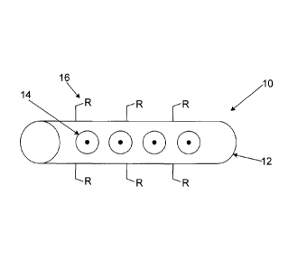
[0052] Figures 1A, 1B and 10 represent probes according to a possible
embodiment
of the invention. Probe 10 has a base structure embodied by capsule 12. This
capsule
plays an important structural role in the probe, but it could also serve as a
spectroscopic
reference when processing the Raman spectrum of the probe.
[0053] The capsule 12 shown in Figures 1A, 1B and 10 has a cylindrical shape.
For
example, a capsule with a cylindrical form could be a carbon nanotube or a
boron nitride
nanotube (BN nanotube). The capsule may also be a small bundle or aggregate of
few
nanotubes. It is noted that the capsule 12 could also have a spherical shape
such as,
for example, a fullerene (C60, C70, etc.) or a conical shape such as, for
example, a
nanohorn, or any other shape known to those skilled in the art. In the case of
a
nanotube, the capsule can be a single wall, double wall or multiwall nanotube.
The
capsule 12 has a nanometric size and, more specifically, the diameter of the
capsule is,
in general, on the order of 0.3 nm to 5 nm. For a nanotube capsule, its length
is, in
general, on the order of 0.5 nm to 1 mm.
[0054] The probe 10 also includes at least one Raman-active molecule 14. As
can be
seen in Figures 1A, 1B and 10, the probe can include more than one Raman-
active
molecule 14, which can be either identical or different from one another.
[0055] As shown in Figure 1A, the active molecules 14 are inserted
(encapsulated) in
the interior of the capsule. This requires that any such active molecule has a
dimension
that permits the molecule to be properly inserted in the capsule and
maintained in the
interior by non-specific van der Waals or electrostatic interactions.
Alternatively, as
shown in Figures 1B and 10, an active molecule can be attached chemically,
electrostatically or physically to the external surface of the capsule 12.
Those skilled in
the art will understand that, for a given capsule, it is also possible to
encapsulate an
13
CA 028270472013-08-09
WO 2012/109761 PCT/CA2012/050099
active molecule in its interior while attaching an active molecule of the same
or of a
different type to its external surface.
[0056] The active molecules 14, also referred to as "dye molecules" or simply
"dyes,"
are molecules that are active in Raman scattering, that is, which can be
detected and
identified by Raman spectroscopy. This is possible if these molecules offer an
optical
resonance in Raman in the wavelength range of an excitation laser of the Raman
apparatus that is used. A large variety of active molecules is therefore
anticipated and
one skilled in the art will be able to identify which molecules to use. For
example, the
active molecules can be derivatives of the type oligothiophenes, of carotenoid
such as,
for example, p-carotenes, methylene violet B having the formula:
9 0
Toluidine Blue, "Fast Black K salt (FBK)", and DTDCI having the formula:
s
C 3
[0057] The oligothiophene type derivatives are, for example, DPP (3,6-
dithiophen-2-y1-
2,5-dihydro-pyrrolo[3,4-c]pyrrole-1,4-dione ) or the DPP derivatives. DPP
derivatives
could be, for example, DPP(2), having the following formula:
TBH,7
I
S
7
r
CBI-117
DPP(2)Br2, having the following formula:
14
CA 028270472013-08-09
WO 2012/109761 PCT/CA2012/050099
CaHi 7
/ KrzN
B
.7
\
CE-117
or DPP(3), having the following formula:
TsH.,
s
'\ I/
0
To this is added the Raman-active molecules such as chromophores or oligomers
based on a 7-type conjugation. For example, there are notably oligomers of
conjugated
polymers such as carbazoles, polyaniline, polyfuranes, polyfluorene,
polypyrroles,
paraphenylen or polyhetero-atomic vinylens. There are also large polyaromatic
molecules such as fullerenes, derivatives of pentacene, anthracene,
peryleneporphyrin,
or naphthalene, etc. and systems well known in Raman resonance such as
benzotriazoles (e.g., 6-tolytriazole), rhodamines (e.g., rhodamine 6G),
pyrolines (e.g.,
pyroline G and thiopyronine), etc. The use of isotope derivatives of these
Raman-active
molecules widens the choice of molecules that will give different Raman
signatures.
[0058] It is noted that the probe 10 can include multiple active molecules
that are
identical or multiple active molecules that are different, each having its own
Raman
resonance. The interest with these more complex probes is to permit a Raman
detection of probes using different wavelengths.
[0059] The probe 10 shown in Figures 1A, 1B and 10 is also functionalized by
chemical groups 16 attached to the exterior of the capsule 12. In Figures lA
and 1B,
the chemical groups 16 are attached directly to the surface of the capsule
while, in
Figure 10, the chemical groups are chemically linked to active molecules that
are
themselves attached directly to the external capsule surface.
[0060] The chemical groups 16 can be of different varieties.
CA 028270472013-08-09
WO 2012/109761 PCT/CA2012/050099
[0061] According to their nature, the groups may also permit a selective
adhesion of
the probe at specific molecular sites of the target material. The chemical
group may be
specific to a given target material, or multi-specific, that is that is can
attach to any one
of a plurality of target materials. Those skilled in the art will understand
how to select the
appropriate chemical groups according to the recommended use of the probe.
There
exist many different functionalization strategies depending on the intended
application.
For example, the addition of positive or negative charges to the capsule with
the groups
such as carboxylic acids or amines permits a selective association with an
oppositely
charged substrate.
[0062] The notable usage of a DNA or RNA group for an association with its
complement or of a protein with its receptor are other good examples for
medical
diagnosis, tagging and scanning applications. According to an embodiment of
the
invention, the chemical group can be a halogenophenyl group, such as
iodophenyl or
bromophenyl. These groups can themselves be easily functionalized to form
other
chemical groups.
[0063] In another example the functionalization chemical group may be a
dispersion
chemical group which facilitate the dispersion of solubility of the probe in a
liquid
material. For example, a lipid membrane medium requires the addition of
aliphatic
hydrophobic groups while aqueous media require instead polar or charged
groups.
[0064] In yet another example the functionalization chemical group can be a
generic
group which can bond with any of a plurality of secondary chemical groups,
which
themselves can attach to the target material. The probe may be provided with
only the
generic functionalization for subsequent specific functionalization, or
already provided
with both the generic and secondary functionalization groups.
[0065] It will be readily understood that a given probe may combine a variety
of
different types of chemical groups, such as dispersion, generic, specific or
multi-specific
to one or several target materials.
[0066] The Raman scattering probes according to some embodiments of the
invention
present numerous advantages such as, for example:
i) The capsule can protect the active molecules encapsulated therewithin. For
example,
carbon nanotubes do not oxidize in normal conditions and are very resistant to
different
16
CA 028270472013-08-09
WO 2012/109761 PCT/CA2012/050099
chemical and thermal treatments. This protection also permits Raman-active
molecules
to resist extreme conditions of heat or chemical corrosion.
ii) By being isolated in the capsule, strong interactions can be prevented
between the
active molecules and the medium in which the probes are dispersed.
Alternatively, and
according to the desired application of the probe, such interactions can be
encouraged
when the active molecules are on the capsule exterior.
iii) Due to the chemical functionalization (covalent or non-covalent) of the
capsule, the
probes can offer very specific chemical affinities. The probes are thus
compatible with a
variety of media and can be adapted to specific applications such as molecular
marking.
iv) The nanometric dimension of the probe as well as the numerous
functionalizing
possibilities provide a great versatility to better target a particular
application. For
example, it can offer the possibility of including chemical groups that act as
recognition
sites for one or more specific substrates.
v) For such a probe, it is possible to attach multiple different functions to
the surface of
the capsule, thus making different applications possible for the same probe.
vi) Embodiments of the probes offer little or no parasitic emission
(fluorescence or
phosphorescence of the molecules) superimposed on the Raman signal. The Raman
optical signal to noise ratio is therefore improved.
vii) Each probe possesses a unique Raman signature and multiple probes can be
differentiated from one another by comparison of their Raman spectra.
viii) The probes can be optimized for one specific excitation wavelength in
choosing
active molecules that are in resonance with the excitation light beam.
ix) Each probe presents an exceptional sensitivity for Raman detection and it
is possible
to obtain a strong signal permitting identification of an individual probe. In
Raman
imaging, it is therefore possible to identify the presence or absence of a
probe at a
precise location with a high spatial resolution of 500 nm or less.
x) Some probes may be composed of one or more active molecules oriented with
regard to the capsule, which confers an anisotropy in the Raman signal with
regard to
the polarization of the excitation light. This anisotropy therefore allows the
measurement of orientation of the probe in the medium.
17
CA 028270472013-08-09
WO 2012/109761 PCT/CA2012/050099
xi) In some embodiments, residues of probe fluorescence combine with the Raman
signature (at a wavelength where there is little fluorescence), allowing a
more sensitive
and specific detection of the probes. It is thus possible to have a coupled
usage of
capsule type probes in fluorescence and Raman.
[0067] As indicated below, the Raman scattering probe according to embodiments
of
the invention can have a wide range of applications, including molecular
marking in
spectroscopy and Raman imaging. In a general context, a Raman scattering probe
as
described above may be functionalized for a particular target molecule, using
either a
functionalization chemical group that bonds directly with the target molecule,
or a
generic chemical functionalization that bonds any of a number of secondary
chemical
groups each of which bonds directly with a different target molecule. When
applied to a
sample material, the probe is attached to a target molecule or a site of
interest within
the sample. The sample is then illuminated with an excitation light beam
having a
wavelength that causes a Raman scattering response in the Raman-active
molecule.
Light from the Raman scattering response is then detected and is indicative of
the
presence of the target molecule. An imaging apparatus may also be used to
detect the
light from the Raman scattering response at a plurality of points across a
surface of the
sample, thus allowing the formation of an image indicative of the relative
location of the
target molecules.
[0068] Some examples of how the probes may be used include medical
applications
for which the probes functionalized by appropriate chemical groups can be, for
example,
used to identify the presence or absence of a membranous receptor on a cell or
a
protein in the blood. In vitro, the probes can be applied to identify a
pathogen or an
unhealthy cell. When specific to a receptor, they can be inserted in a living
being and
serve as a tool for establishing a medical diagnosis or for localizing the
presence of
unhealthy or cancerous cells. Moreover, these probes can be used as contrast
agents
in biomedical Raman imaging.
[0069] In other specific applications such as, for example, in the area of
civil security
and/or forensics, the probes can be used for detecting trace compounds such as
explosives, drugs, DNA, RNA, proteins or hormones. These Raman probes can also
be
used in the identification of documents. The insertion of a specific probe in
the material
18
CA 028270472013-08-09
WO 2012/109761 PCT/CA2012/050099
of the document and the identification of it by Raman analysis of the document
offers
rapid means of obtaining solid proof of the authenticity of a document.
[0070] As a research tool, the probes according to the invention can serve as
optical
tracers for studying complex processes such as metabolism and physio-chemical,
biochemical and biological systems. The notable use of probes in a
microfluidic system
allows the localization by Raman measurement of the presence or absence of a
substance or a cell in one of the channels of the device. This identification
can be used
for further tasks such as sorting, derivation or labelling the substance or
the cells.
Description of Preparation Methods According to Embodiments of the Invention
[0071] In accordance with another aspect of the invention, there is also
provided a
method of preparing a Raman scattering probe.
[0072] Figure 2 shows the different steps for the method of preparing a Raman
scattering probe as described above. The method includes a first step of
providing a
capsule of nanometric size. Optionally, the method may involve cleaning and
opening
the unprocessed nanometric capsule. According to an illustrative embodiment,
this step
may involve a cleaning of the capsules by reflux in concentrated nitric acid.
The
treatment in nitric acid allows both the cleaning and the opening of the
capsules to
enable the subsequent encapsulation. After the cleaning and opening of the
capsules,
it is desirable to filter them with a porous membrane using a vacuum pump and
to air-
dry them. The capsules thus dried are removed from the filter and can
thereafter be
placed in deionized water for subsequent hydrothermic treatment. At the time
of this
treatment, the capsules are functionalized by oxidized groups such as -COOH, -
OH and
=0. The hydrothermic treatment occurs generally under reflux and constant
agitation in
a period of about three hours. The aqueous phase is thereafter eliminated by
filtration.
The capsules are then cleaned using a solvent and dried in a vacuum. An
example of
this detailed procedure is presented below for the cleaning and opening of
carbon
nanotubes. The capsules may also be shortened by cutting them using an
ultrasonic
treatment in a liquid or in an acid solution, and sorted by size or by
material properties
(such as whether metallic or semiconductor) using chromatography or
ultracentrifugation in a density gradient.
19
CA 028270472013-08-09
WO 2012/109761 PCT/CA2012/050099
[0073] In a second step as shown in Figure 2, one or more Raman-active
molecules
are coupled to the capsule. In some embodiments, this coupling may be
accomplished
by either insertion in the capsule (encapsulation) or linked by a chemical
bond to the
external surface of the capsule, thereby forming a capsule-active molecule
composite.
It is also possible that active molecules are both encapsulated in the capsule
and
attached to its external surface.
[0074] Encapsulation can be done in vapour phase or liquid phase. In one
embodiment, the gaseous method is preferably done in a container, such as an
ampoule, under vacuum. The container is filled with the clean and opened
capsules
and with a supply of molecules to encapsulate. A simple heating of the
container to the
sublimation temperature of the molecules to be encapsulated induces the
encapsulation. A complete encapsulation takes generally several hours. The non-
encapsulated molecules are then removed using solvents or by sublimation of
the free
molecules. The method of liquid phase encapsulation involves dispersing the
open
capsules in a solvent containing the molecules to be encapsulated dissolved
therein to
saturation. A reduction of the solubility of the molecules to be encapsulated
in the
solvent is thereafter carried out by slow reduction of the temperature, by
slow
evaporation of the solvent or by the slow replacement of the solvent by
another solvent
that is less favorable to the solubility of the active molecules. The
encapsulation in
liquid or vapour phase is a spontaneous thermodynamic process.
[0075] In other embodiments, the chemical association of the active molecule
on the
external surface of the capsule can be done with a carbon-carbon coupling
reaction
using a free radical reaction of the molecule with the capsule. More details
on this type
of reaction are given below such as, for example, in the case of a carbon
nanotube
probe having attached to its external surface an active molecule of toluidine
blue.
[0076] In a third process step for preparing the probes according to the
present
invention, at least one functionalization chemical group is attached to an
external
surface of the capsule. This functionalization makes the probe compatible with
a liquid
or aqueous medium or a receptor or both. For this, a functional group R is
attached
directly to the capsule or attached to an active molecule that is attached to
the exterior
of the capsule. The functionalization by the functional group is, in general,
CA 028270472013-08-09
WO 2012/109761 PCT/CA2012/050099
accomplished by covalent bonding in an aqueous medium or in a solvent with
free
radical reagents. An example of a free radical reagent is a
phenyldiazoniumsalt or
aderivative of the diazonium salt. The invention is not limited to these
reagents and one
skilled in the art will know how to choose other types of reagents providing
addition
reaction to the capsule. The excess of reagents are subsequently eliminated
using, for
example, a solvent and filtration with a PTFE membrane. Subsequent reactions
with
the groups enable different varieties of functionalization. The choice of
chemical group
depends on the particular application intended for the probe. Details of some
reactions
possible with carbon nanotubes are presented below. General information is
also
available in recent literature on chemical attachment to carbon nanotubes.
[0077] Functionalization by a chemical group R attached to the capsule can be
either a
"generic" functionalization or a "target-specific" functionalization. A target-
specific
functionalization involves a chemical group that is both attached to the
capsule and that
attaches directly to a target molecule of interest, that is, a molecule that
is to be tagged
by the probe. While the target-specific functionalization allows the direct
bonding
between the probe and the target, it requires that the probes be developed
individually
for each marking application. In another embodiment of the invention, a probe
may
instead be formed with a "generic" functionalization that may be subsequently
modified
to render it specific to a particular target.
[0078] The concept of a generic functionalization is known in the art with
regard to
other types of molecular markers. In such a case, the functionalization
provided with
the probe is not one that is target specific but, rather, one that may be
easily linked to
another chemical group that is target specific. Thus, referring again to
Figures 1 and 2,
the chemical group R, if generic, would have a chemical structure that allowed
the easy
attachment of a wide variety of possible secondary chemical groups that, in
turn, were
target-specific. Thus, the generic functionalization and the additional
chemical group
would together function as the link between the capsule and the target
molecule. In this
way, probes with a generic functionalization can be produced in large
quantities and
subsequently tailored to a specific application.
[0079] One example of a generic functionalization makes use of the compound
polyethylene glycol (PEG). Variants of this compound may be used to attach to
the
21
CA 028270472013-08-09
WO 2012/109761 PCT/CA2012/050099
external surface of the capsule, and have a chemical structure that bonds
easily with
other chemical groups. Thus, a probe produced with a PEG-based
functionalization
may be modified by a user to attach a desired target-specific chemical group
and
thereby render the probe target-specific.
[0080] Finally, a non-covalent functionalization with surfactants or polymers
such as
pluronic or PEG can also be implemented so as to better stabilize the probes
in the
aqueous medium. In this case, slight oxidation of the capsule at the time of
the cleaning
step is useful for stabilizing the surfactant-capsule composite. This step
involves the
addition of a surfactant (or a polymer) to the solution of probes and a
subsequent
activation of the mixture by an ultrasound treatment. A final step of
centrifugation
serves to keep the probes in solution for extraction of the largest
aggregates. This
procedure is used for dispersing the carbon nanotubes.
[0081] According to another embodiment of the method for obtaining the probes
according to the present invention, the third step described above is
implemented
before the second step. In effect, it is possible to functionalize the capsule
by the
chemical group R before forming the capsule-active molecule composite.
[0082] It is possible to develop a very large variety of different Raman
probes using
the method described above. The number is almost infinite and depends on the
application and the wavelengths anticipated and available for use with the
Raman
instrument.
Examples of Encapsulated Raman Probes and their Methods of Fabrication
[0083] In the following examples, Raman scattering probes according to the
invention
were prepared using single wall carbon nanotubes each having a diameter of -
1.4 nm
and lengths between 100 nm and 5 im or more. The chemical group attached to
the
surface of the nanotube is bromophenyl or phenyldiazonium group. Different
active
molecules were encapsulated in the SWNT, such as is described in detail below.
Another type of probe was also prepared using double wall carbon nanotubes
(DWNT).
In this case, toluidine blue is used as an active molecule and is fixed by
covalent bond
to the external surface of the nanotube.
22
CA 028270472013-08-09
WO 2012/109761 PCT/CA2012/050099
[0084] The inventors have determined that individual SWNT probes chemically
functionalized with dyes show exceptional Raman scattering properties.
Depending on
the position of the dye, external or internal to the carbon nanotube, a
general protocol of
synthesis in three steps is used: i) opening and cleaning of the nanotubes;
ii)
encapsulation of the dye; and iii) covalent reaction on the external layer.
The details
concerning the step of encapsulation are specific to the dye used, but steps
i) and iii)
are the same for all the probes.
i)Protocol of Opening and Cleaning of the Nanotubes
[0085] All of the nanotube samples were washed beforehand by ref lux in
concentrated
nitric acid. This protocol allows the cleaning of the nanotubes, the
functionalization with
-COOH groups and the opening of ends of the nanotubes to allow the
encapsulation.
The procedure used is as follows: a mass of 100 mg of unprocessed SWNT is
placed in
300 ml of 67% nitric acid (Fisher). The mixture is heated to ref lux under
constant
agitation for a period of four hours. The nanotubes are then filtered with a
1.22 pm
PTFE membrane using a vacuum pump. The resulting film, generally referred to
as
"buckypaper", is air-dried. It is subsequently removed from the membrane and
placed
in 300 ml of deionized water (18.2 MO - Millipore) to undergo a hydrothermic
treatment.
As with the acid treatment, this treatment proceeds under reflux and constant
agitation
for a period of three hours. The aqueous phase is eliminated by filtering with
a 1.22 pm
PTFE membrane. The "buckypaper" is finally washed with a solvent and dried
under
vacuum until it may be easily removed from the membrane. Generally, the final
mass of
carbon nanotubes is between 40 mg and 60 mg.
iii) Protocol of Covalent Functionalization of the External Surface of the
Carbon
Nanotubes with a Chemical Group R
[0086] The reaction of functionalization is implemented in an aqueous medium
having
a weak concentration of phenyldiazonium. A deoxygenated solution of
tetrafluoroborate
4-bromophenyl diazonium 0.79 mM (96%, Sigma-Aldrich) at a pH - 10 is first
prepared.
The adjustment of the pH is realized by an addition of sodium hydroxide. The
23
CA 028270472013-08-09
WO 2012/109761 PCT/CA2012/050099
encapsulated SWNT are then immersed in a solution for ten minutes under
agitation at
room temperature, and are finally rinsed with deionized water and
diethylether.
[0087] Multiple variants of these functionalizations (i.e., using different
chemical
groups R) are possible so as to adapt the capsule probes for one application
or another.
For example, an attachment of toluidine blue, a Raman-active molecule, to the
exterior
of the capsule is possible using a covalent reaction on the group R remaining
from the
step of functionalization by diazonium salt (preceding step). Another example
demonstrated by the inventors is the attachment of a negatively charged
chemical
group to the same group R to allow the selective assembly of nanotubes on a
surface.
The variations of functionalization are practically infinite and depend on the
anticipated
application.
EXAMPLE 1: Probes of the type oligothiophene@SWNT
a) Probes a¨sexithiophene@SWNT
[0088] The assembly of a-sexithiophenes(6T) in carbon nanotubes is known in
the
prior art. [M. A. Loi, J. Gao, F. Cordella, P. Blondeau, E. Menna, B Bartova,
C. Hebert, S.
Lazar, G. A. Bolton, M. Milko, et C. Ambrosch-Draxl, Adv. Mater. 22, 1-5
(2010)]Figure 3A
illustrates the encapsulation of 6T in the nanotube and shows schematically
the large
size of the capsule relative to the molecules.
[0089] Measurements of absorption and Raman scattering on the powder form of
6T@SWNT composites, of a solution containing them and on the samples of
individual
6T@SWNT composites deposited on a silicon substrate, were done by the
inventors.
To disperse the 61@SWNT deposits in a solvent solution, the samples were
functionalized by chemical oxidation in concentrated HNO3. This step permits
the
attachment of COOH functions on the exterior of the nanotubes. The absorption
spectrum of the functionalized 6T@SWNT powder, shown in Figure 3B, has a
principal
absorption band located at about 510 nm and several other absorption bands
between
600 nm and 1200 nm. The band at 510 nm is associated with dye molecules of 6T,
while the other bands (900-1200 nm and 600-800 nm) are associated with the
optical
absorption of carbon nanotubes. The Raman spectra of these signals were
measured
at different excitation wavelengths (782, 633, 514, and 488 nm, as indicated
in Figure
24
CA 028270472013-08-09
WO 2012/109761 PCT/CA2012/050099
3B). The individual Raman spectra of the sample powder at each of the
excitation
wavelengths are presented in Figure 4. Figure 5 shows the spectra of Figure 4
in the
region around 1500 cm-1 and compares them to the spectra obtained for the
unprocessed carbon nanotubes. In this figure, the spectra of the 6T@SWNT
composites are indicated by reference numeral 50, while the spectra of the
unprocessed carbon nanotubes are indicated by reference numeral 52. The band
located around 1457 cm-1 in the Raman spectrum is the most distinct signature
of the
encapsulated a-sexithiophene. A comparison with the spectra of nanotubes
without the
dye allows an identification of the other less-intense bands associated with
the
nanotubes. The signal from the dye is more intense than that of the nanotubes
when
the excitation wavelength is close to, or directly in resonance with, the dye,
at either 633
nm, 514 nm or 488 nm. However, at 782 nm, the signal attributable to the 6T is
less
intense relative to that of the nanotubes. These measurements illustrate the
resonant
character of the process of Raman scattering with the 6T@SWNT. Figures 4 and 5
show that there is a resonant process because the Raman signal of the a-
sexithiophene
is much more intense only when the wavelength of the excitation energy is near
that of
the absorption energy of the a-sexithiophene.
The Raman measurements of the 6T@SWNT composite allow observation of a strong
Raman signal coming from the molecules and determination that resonance is
essential
for maximizing Raman scattering. However, a measurement of the powder does not
allow a determination of whether the Raman scattering of the molecules is
strong or not.
In this first experiment, the inventors have nevertheless noticed that there
is no
fluorescence signal, even beyond the zone of the spectrum presented here. This
characteristic makes measurement of the spectrum easy to achieve because there
is no
fluorescence noise. To determine the strength of the Raman signal, the
inventors
performed supplemental experiments on the individualized 6T@SWNT. The results
presented in Figure 6 demonstrate that the Raman signal of the molecules at
the
resonance energy is stronger than that of the nanotubes. This experiment is
performed
on a small bundle of a-sexithiophene nanotubes that have a length of
approximately
one micron and that are positioned on a surface of silicon oxide. The AFM
image of the
probe is shown at the left in Figure 6. The local Raman measurement at the
position of
CA 028270472013-08-09
WO 2012/109761 PCT/CA2012/050099
this probe is shown at the right in Figure 6. The band associated with the dye
and its
intensity at 633 nm is clearly visible in the spectrum. The intensity is
higher than that of
the nanotube. With this measurement, it may be concluded that the Raman signal
of
the a-sexithiophene molecules is generally stronger than or similar to that of
the
nanotubes. As the cross section of the nanotubes is aR-1 0-22 cm2, this
measurement
demonstrates that the cross section of the molecules in the beam is important.
This
measurement allowed the inventors to conclude that this type of composite
presents
outstanding properties and that it is very interesting for obtaining strong
Raman signals.
Raman Scattering Cross Section of a-sexithiophene@SWNT Probes
[0090] A first way to estimate the cross section of the Raman scattering of
molecules
in Figure 6 is to use the Raman scattering of the nanotubes as an internal
reference. It
is believed that the scattering cross section of the nanotubes is in the range
between
3x10-23 to 3x10-22 cm2/sr. As the signal coming from the molecules is about
three times
more intense than that associated with the nanotube, it is possible to deduce
that the
cross section of the collection of molecules under the beam is in the range of
10-22 to 10-
21 2
cm-/sr. The number of molecules in the exposed nanotubes under a beam having a
diameter of 500 nm is approximated to be 455 per nanotube. Assuming that there
is the
equivalent of one nanotube completely filled with molecules, the cross section
per
molecule is between 2 x 10.25 and 2 x 10-24 cm2/sr. Albeit approximate, this
estimate is
reasonable because the bundle contains, in reality, from 3 to 5 nanotubes, but
these are
partially filled by the molecules. It is noted that a cross section of 10-24
cm2 per
molecule is typical for a resonance process in Raman for dyes such as a-
sexithiophene.
The typical area of a molecule in this composite being 1.4 nm x 4.47 nm/4 =
1.57 x 10⁻⁶
prn2 (or 1.57x10⁻¹⁴ cm2), it is necessary to count about 1011 ¨ 1010 photons
per molecule
per nanotube to obtain a Raman signal.
[0091] This estimate of the cross section per molecule can be validated from
measurements of laser power used to make the measurement. From earlier
experiments, the laser light at a 514 nm wavelength and at 14.5 mWof power
offers a
power at the output of the 100X objective of about 2 IN at 100% and of about
1 jiW at
50%. For the laser at 633 nm (13 mW), there was approximately 2 mW at the
output of
26
CA 028270472013-08-09
WO 2012/109761 PCT/CA2012/050099
the 100X objective at 100% and about 1 mW at 50%. The numerical aperture of
the
100X objective is 0.9 (angle of 65 or 1.13 sr) and the size of the spot is
about 500 nm.
The power in the case of Figure 6is 2mW on a spot having a diameter of 500 nm
(or an
energy density of -106 W/cm2) and the exposure time for the spectrum is 30
seconds.
This energy density corresponds therefore to a density of 7x10¹⁷ photons jm2.
(i.e., 30
seconds at 2 x 10¹⁶ photons/s/ m2). As the section of the nanotube under the
beam is
only 0.5 pm long and 1.4 nm wide, the total quantity of photons for the
measurement of
the spectrum is only -6 x 10¹⁴ photons. The quantity of molecules is about
455, which
gives a density of 1012 photons per molecule. This value is similar to an
earlier estimate.
Any difference may be attributed to the limited efficiency of the detector and
to the loss
of photons by the transfer optic.
b) Probes DPP@SWNT
[0092] Other probes based on encapsulated oligothiophene were fabricated so as
to
investigate the fabrication of active probe at other resonance energies. The
inventors
prepared DPP composite probes that, as indicated below, allow an adjustment of
the
resonance energy at various positions in the visible spectrum. DPP (DPP1, DPP2
and
DPP3) are analogs to polythiophene that offer interesting resonances in the
wavelength
range from red (near 633 nm) to blue (514 nm). These molecules offer a great
flexibility
of synthesis. The reaction diagram shown in Figure 7 illustrates the steps for
synthesizing DPP composites used for encapsulation in SWNT. In the diagram,
DPP2
is the compound (6) and DPP3 is the compound (7).
[0093] The preparation of these DPP@SWNT probes involves first cleaning and
openingcarbon nanotubes in the manner described above. For the encapsulation,
2 mg
of cleaned and opened SWNT are dispersed in 20 ml of DMF by sonication for
thirty
minutes, after which 10 mg of DPP dye is added and the solution is treated
with
ultrasound for another five minutes. The solution is heated to reflux
overnight in a
nitrogen atmosphere. The sample is harvested by filtration after ten washes
with THF
with gentle sonication for three minutes between the washes to disperse the
tubes
following a filtration and ten other similar washes with DMF. The
functionalization of
these composites with the group R proceeds according to the protocol described
above.
27
CA 028270472013-08-09
WO 2012/109761 PCT/CA2012/050099
[0094] The fabrication of probes DPP3@SWNT, DPP2@SWNT and DPP1@SWNT
was done in steps. For each step, the Raman spectra were measured. Figures 8A
and
8B show examples of Raman spectra measured during the synthesis steps for the
probe DPP2@SWNT. In Figure 8A is shown the spectra at 633 nm with and without
the
step of opening of the SWNTs. In the figure, reference numeral 70 indicates
the DPP2
spectrum with the SWNT opened, and reference numeral 72 indicates the spectrum
with the SWNT unopened, which contains no DPP signal and only SWNT Raman
peaks.
[0095] It is noted that these spectra show clearly that the opening and
cleaning step is
essential to obtain a strong signal of the DPP molecules. The final step of
functionalization with the chemical group R (here R = bromophenyl), as shown
in Figure
8B, demonstrates that the Raman spectrum remains almost identical to that
measured
before this step. In this figure, the DPP2@SWNT spectrum without the chemical
group
R is identified by reference numeral 80, while the DPP2@SWNT spectrum with the
group R is identified by reference numeral 82.
[0096] This experiment shows that the covalent reaction on the external
surface of the
SWNT causes little or no modification of the Raman spectrum. Figure 9 shows
the
Raman spectra of three probes DPP3@SWNT, DPP2@SWNT and DPP1@SWNT at
excitation wavelengths of 633 nm, 633 nm and 514 nm, respectively. While the
functionalization does not affect the Raman response, nevertheless, it is
clearly
illustrated when one compares the dispersion or solubility of probes in a
solvent. A non-
functionalized probe is insoluble in a liquid such as DMF and forms an
insoluble
precipitate. A probe functionalized by the chemical group R disperses easily
in a
solvent and forms a stable suspension without aggregation. Moreover, a
spectroscopic
measurement of photoemission X (by XPS) allows confirmation that the
attachment of
the chemical group R is successful.
EXAMPLE 2: Encapsulated Raman Scattering Probes with Commercial Molecules
[0097] Multiple capsule probes can be made using commercial molecules. The
choice
of a Raman-active molecule is made based on the Raman resonance energy and the
spectral characteristics necessary for a given application. There is a wide
variety of
28
CA 028270472013-08-09
WO 2012/109761 PCT/CA2012/050099
different molecules available, and the inventors have worked with such
molecules as
methylene violet B and diethylthiodicarbocyanine iodide (DTDCI).
[0098] a) Methylene violet B@SWNT Probes
[0099] Capsule probes prepared with methylene violet B have been shown to
provide
a good response in Raman scattering. Methylene violet B possesses the
following
structure:
1-sC
[00100] The process of fabrication follows the general steps described. For
the
encapsulation step, an abundance of the SWNT and the methylene violet B are
dispersed in heptane and the suspension is treated with ultrasound for about
two
minutes. The suspension is then agitated overnight to ref lux, and is
subsequently
purified by successive cleanings with DMF. This step is terminated when the
filtrate
remains only very slightly colored or when the Raman spectra recorded before
and after
the last washing session are equivalent.
[00101] An example of a Raman spectrum at 633 nm of the methylene violet
B@SWNT probe obtained after the synthesis is shown in Figure 10 and indicated
by
reference numeral 100. The Raman signature of the probe is also compared with
that
of methylene violet B powder, for which the spectrum is also shown in Figure
10 and
indicated by reference numeral 102. Differences between the spectra are
noticeable,
particularly in the region surrounding 1500 cm-1. These differences come from
the
encapsulation of the molecules in the SWNT probe.
29
CA 028270472013-08-09
WO 2012/109761 PCT/CA2012/050099
[00102] b) DTDCI@SWNT Probes
[00103] The fabrication of probes with diethylthiodicarbocyanine iodide
(DTDCI) also
worked well. These probes were also prepared according to the general protocol
described above. The structure of DTDCI illustrated below is that of a
conjugated linear
molecule that offers a good polarizability and, therefore, good response in
Raman
diffusion in the visible range.
N- s
(CH;
[00104] For the encapsulation step, the SWNT are dispersed with an abundance
of
DTDCI in water, followed by an ultrasonic treatment for about 15 minutes. The
solution
is then brought to reflux under agitation for twenty hours. Multiple cleanings
using DMF
were done until complete extraction of the non-encapsulated dye was achieved
(i.e.,
until the filtrate is uncolored).
[00105] The Raman spectrum at 633 nm of the DTDCI@SWNT probe obtained after
the synthesis is shownin Figure 11 and is indicated by reference numeral 110.
The
Raman spectrum of the probe is also compared with that of DTDCI powder, which
is
also shown in Figure 11 and indicated by the reference numeral 112. The
differences
between the two spectra are noticeable. These differences come from the
encapsulation of the molecules in the SWNT.
EXAMPLE 3: Toluidine Blue ¨ DWNT Probes (external dye attachment)
[00106] An example of a capsule probe such as that shown in Figure 1B was
achieved
using toluidine blue as the Raman-active molecule. For this probe, the Raman-
active
dye is chemically attached by a covalent reaction to the exterior of the
nanotubes and,
more particularly, to the external surface of the capsule.
CA 028270472013-08-09
WO 2012/109761 PCT/CA2012/050099
[00107] The fabrication method uses one variation of the general method
presented
above. Because the step of encapsulation is not necessary for these probes,
that step
is omitted, and the process goes directly to the chemical attachment of the
dye to the
capsule. For the toluiding blue-DWNT probe, one part double wall nanotubes
(DWNT)
and four parts toluidine blue are placed in a round-bottom flask. The flask is
purged
with nitrogen and heated to 1302C. Thirty parts of isoamylnitrite are then
added to the
mixture and the reaction proceeds for 24 hours under vigorous agitation. The
residue
that contains toluidine blue-DWNT is rinsed with water twice and washed
subsequently
multiple times with DMF until the free dye is completely removed ( free
toluidine blue
being very soluble in DMF). The washing is done by an ultrasonic treatment for
10
minutes of the residue of the reaction in the DMF. The product is then
harvested by
filtration and drying with THF.
[00108] A variation of this reaction which gives the same result uses a
reaction in
liquid phase instead of the solid state. The procedure in the liquid phase is
the same
except that the quantity of isoamylnitrite is 45 parts (instead of 30) and the
anhydrous
DMF is added to the medium at the proportion of 200 parts. The diagram of the
insertion reaction of the toluidine blue by external attachment to the
nanotubes is shown
in Figure 12A (where "CNT" represents the carbon nanotubes, and "DMF
(anhydre)"
refers to the anhydrous DMF).
[00109] The spectrum at 633 nm of the toluidine blue-DWNT probe, obtained
after the
solid synthesis, is shown in Figure 12B and is indicated by reference numeral
120. The
Raman spectrum of the probe is compared with that of the double wall nanotubes
(DWNT), which is also shown in Figure 12B and indicated by reference numeral
122.
Additional bands around 500 and 1400 cm-1 are noticeable in the spectrum of
toluidine
blue-DWNT. These bands come from a Raman signal of toluidine blue molecules
attached chemically to the DWNT.
Detailed Investigation of a-sexithiophene Probes
[00110] In another experiment conducted by the inventors, Raman probes were
produced that consisted of a-sexithiophenes (6T) encapsulated within phenyl-
functionalized SWNT (6T@f-SWNT). A detailed study with Raman was carried out
in
31
CA 028270472013-08-09
WO 2012/109761 PCT/CA2012/050099
situ at each step of the preparation procedure. The general steps of this
procedure are
illustrated schematically in Figure 13. In a first step, the nanotubes 130
were processed
by acid and ultrasound and encapsulated in a liquid phase with 6T molecules.
The
resulting 6T@SWNT 132 were then functionalized with either iodophenyl or
bromophenyl groups by covalent addition using diazonium salts. This procedure
yields
the 6T@f-SWNT product 134 with the phenyl grafts, as indicated in the figure.
Shown at
136 in Figure 13 is a more detailed illustration of the 6T aligned inside a
nanotube. The
arrow shown in the figure indicates the directional Raman polarizability of
the
molecules.
[00111] In preparing the 6T@f-SWNT probes, only reagent grade solvents were
used.
4-bromobenzenediazonium tetrafluoroborate (96%, Aldrich), 4-
aminopropyltriethoxysilane (APTES) (99%, Aldrich),isopentyl nitrite (96%,
Aldrich), and
the a-sexithiophene (Aldrich) were used as received. 4-lodoaniline (98%,
Aldrich) was
recrystallized from hexanes before use. The SWNT were produced by laser
ablation.
[00112] For the encapsulation of a-sexithiophene in SWNT (6T@SWNT), the SWNT
first were purified using concentrated nitric acid wet chemical oxidation and
cut by
exposing the SWNT to piranha solution (3:1 conc. H2504/H202) for three hours.
The
SWNT were filtered on a PTFE filter (1.2 pm pore size), and were thoroughly
washed
with water. 55 mg of the nanotube residue was then dispersed in DMF, filtered,
dispersed in THF, filtered, and rinsed with toluene. 12 mg of 6T was
thereafter added to
mL of toluene and sonicated for five minutes. The buckypaper obtained by
filtration
was added to the 6T solution, and sonicated for two minutes and refluxed at
115 C for
48h0urs. The encapsulated SWNT were filtered on a PTFE filter (0.45 pm), and
dispersed in 15 mL DMF. Dispersion and filtration of the nanotubes was
repeated five
times to removed free 6T molecules. The resulting buckypaper of 6T@SWNT was
subsequently characterized by Raman spectroscopy.
[00113] The iodophenyl functionalization of 6T@SWNT (6T@f-SWNT) was done on 1
mg of 6T@SWNT and 75 mg of iodoaniline, which were purged in nitrogen followed
by
the addition of 20 kIL of isopentylnitrate. The reaction was heated to 802C
for three
hours, and the mixture was then diluted in 25 mL of DMF and filtered. The 6T@f-
SWNT
32
CA 028270472013-08-09
WO 2012/109761 PCT/CA2012/050099
were washed in DMF until the filtrate was free of iodoaniline, as measured by
thin layer
chromatography.
[00114] An aminopropyltriethoxysilane substrate (APTES) was formed on a
patterned
SiO2/Si substrate. Preparation of this substrate began with a substrate of
silicon having
a 100 nm oxide (SiO2/Si). An electrode pattern was created using standard
photolithography followed by e-beam evaporation of titanium (0.5 nm) and
palladium (25
nm). This pattern was used to identify individual nanotubes on the substrate
and
allowed location of the same structure with the Raman after each modification.
A
substrate cleaning procedure consisted of successive sonication of five
minutes each in
acetone and isopropanol (IPA). The substrates were then placed in a glass
desiccator
and vacuum dried for at least ten minutes. The substrates were then placed on
glass
slides suspended above a small crystallization dish containing one millilitre
of APTES.
The desiccator was vacuum pumped for one minute and the chamber was sealed for
an
additional thirty seconds. Finally, the APTES layer was annealed in air for
twenty
minutes at about 100 C in a conventional oven.
[00115] The SWNT were then deposited on the APTES patterned substrate.
Purified
SWNT were suspended in N,N-dimethylformamide (DMF) and diluted as needed. The
SWNT were spin-coated onto the APTES substrate at a speed of 7000 rpm from the
DMF suspension to obtain about 1 nanotube/3 m2.
[00116] To perform the encapsulation yielding the 6T@SWNT, the SWNT on the
substrate were dipped in DMF, THF and toluene to remove water. 12 mg of 6T was
then mixed with 5 mL of touene in a round bottom flask and sonicated for five
minutes.
The substrate covered with SWNT was gently placed into a flask equipped with a
condenser and the solution was refluxed at 115 C for 24-48 hours. Residual 6T
was
removed from the surface by first sonicating in fresh toluene and sonicating
in DMF.
The sample was then rinsed with IPA and nitrogen-dried before characterization
by
atomic force microscopy (AMF) and Raman spectroscopy.
[00117] The functionalization of the 6T@SWNT to give 6T@f-SWNT started with a
2
mM 4-bromobenzenediazoniumtetrafluoroborate prepared with 20 mL of degassed
milliQ water (pH - 10). 6T@SWNT was then placed into the aqueous salty
solution for
ten minutes and rinsed in water and IPA, and dried using a nitrogen flow.
33
CA 028270472013-08-09
WO 2012/109761 PCT/CA2012/050099
[00118] To create a layer of 6T@SWNT in a cross pattern (the results of which
are
discussed below in conjunction with Figure 16), APTES was deposited on a SiO2
substrate as described above. A suspension of 1 mg/mL of 6T@SWNT in DMF was
then prepared by sonicating for 10 min. The APTES substrate was immersed into
the
6T@SWNT dispersion for thirty minutes at room temperature, and was then rinsed
with
DMF before being immersed in hot DMF for two minutes. The nanotube-covered
substrate was rinsed with IPA and blow dried with nitrogen. A layer of Shipley
S1805
photoresist was then spin-coated onto the nanotube-covered substrate, and a
cross
pattern was defined using photolithography. The unprotected regions were
removed by
an oxygen reactive ion etch (30 s, 125 mTorr, 80 mW/cm2), and the substrate
was
plunged into remover to reveal a cross pattern of 6T@SWNT. This pattern was
then
characterized using SEM images and Raman spectroscopy.
Measurement of the 6T@f-SWNT Probes
[00119] The experimental results shown in Figures 14A-16 were acquired on
individualized SWNT deposited on an oxidized silicon substrate, on a sub-
monolayer of
6T@SWNT on an oxidized silicon substrate and patterned by optical lithography
in a
cross pattern or on bulk 6T@f-SWNT dispersed in an inorganic oil. These
spectra
were recorded at each step of the procedure using absorption and Raman
spectroscopy. The structures of the probes were also investigated using AFM
and
SEM.
[00120] The AFM images were produced using a Dimension 3100 scanning probe
microscope equipped with a Nanoscope IV controller and a quadrex extender
module.
Height images were acquired using intermittent-contact mode using silicon
probes of
nominal spring constants of 42 Nm-1, a resonance frequency of - 320 Hz, and a
tip
radius curvature < 10 nm.
[00121] The Raman spectrometer used is a custom-built instrument with three
different excitation laser lines (2.54, 2.45, 1.94 eV), a 100x objective and a
nitrogen
cooled charged-coupled device camera (JY Symphony). The sample stage was
equipped with a 3-axis piezoelectric displacement stage. The laser power on
the sample
was -95 W pm-2. Spectral region probe was between 1200-1700 cm-1 in the D and
G
34
CA 028270472013-08-09
WO 2012/109761 PCT/CA2012/050099
regions of the SWNT with a precision of 1 cm-1. The Raman mapping was
performed
with 1 turn steps in the X and Y axis. Each point was integrated for five
seconds with a
laser power of 300 W pm-2.
[00122] Absorption spectra of the SWNT, 6T@SWNT and 6T@f-SWNT bulk dispersed
in inorganic oil are shown in Figure 14B. As shown, the absorption of the 6T
is intense
and structured in the 350-700 nm region. The 6T@SWNT has an absorption
spectrum
that combines the 6T and SWNT absorption features with no significant shift in
the
resonant absorption peaks. The 6T@f-SWNT shows a spectrum that is similar to
the
61@SWNT except that the absorption of the SWNT is weaker because of the
grafting of
the phenyl groups onto the SWNT sidewalls.
[00123] For the Raman spectrum shown in Figure 14A, an individual and isolated
SWNT was previously located on the oxidized silicon substrate and identified
by AFM
and Raman. Its apparent height in AFM is 1.2 nm, which corresponds to the
diameter of
an individual nanotube. For each step of the procedure, Raman spectra in
Figure 14A
were taken at the same location and using the same polarization conditions.
Before
encapsulation (top spectrum), the shape of the Raman G mode at -1590 cm-1
confirms
the presence of a semiconducting SWNT. The presence of a single RBM mode (not
shown) is consistent with a signal coming from an individual SWNT. After
encapsulation
(middle spectrum), the Raman peaks characteristic of 6T molecules appeared
strong
and clear in the spectra of 6T@SWNT. The most intense peak of the 6T at 1450
cm-1 is
assigned to the main component of the C=C stretching mode propagating along
the
main axis of the molecule. The presence of this Raman mode unambiguously
reveals
the presence of 6T molecules. An inspection of the area around the 6T@SWNT
indicated no signal, which implies that the molecular signal is only from the
6T@SWNT
structure, not from other 6T molecules adsorbed on the surface. The Raman
spectra
taken after the bromophenyl functionalization step on the individual 6T@SWNT
is
shown in the bottom spectrum of Figure 14A. The intensity of the 6T peak is
preserved
whereas the G mode of the SWNT at -1590 cm-1 decreases in intensity. The
appearance of a defect mode, called the D-mode, of the SWNT at -1330 cm-1
indicates
that there is an interaction between the molecules (6T and grafts) and the
SWNT. The
change of the SWNT modes in the spectrum and the absence of any change for the
6T
CA 028270472013-08-09
WO 2012/109761 PCT/CA2012/050099
signal proves that the SWNT has been functionalized with the bromophenyl
adducts
and that the 6T are located inside the nanotube.
[00124] In another set of experiments, two individual 6T@SWNT deposited on an
oxidized silicon substrate were first located using micro Raman spectroscopy
and AFM
imaging (Figures15A-15B). The Raman spectrum associated with each SWNT capsule
presents distinct resonances with excitation energy, which indicates that one
is metallic
(Figure 15A) and the other is semiconducting (Figure 15B). For our laser
ablation
SWNT sample, such identification is possible because only metallic SWNT are
resonant
in Raman at 1.94 eV (Figure15A) whereas semiconducting SWNT are resonant only
at
2.33 eV and 2.54 eV (Figure 15B). At 2.33 and 2.54 eV excitations, the
individual
metallic 6T@SWNT has an intense 6T peak at 1460 cm-1 and there is almost no
signal
from the SWNT capsule. Thus, the SWNT is out of resonance while the 6T is
clearly in
resonance, which is consistent with the absorption spectra in Figure 14B. At
1.94 eV
excitation, the opposite is observed: The 6T signal is weak and the SWNT is
strong.
The Raman signals of the SWNT and 6T are therefore uncorrelated from each
other
and simply follow the resonance pattern, as in the absorption spectrum.
Moreover, one
can clearly see that the presence of a SWNT resonance does not significantly
contribute to the enhancement of the 6T Raman signal. For the individual
semiconducting 6T@SWNT (Figure 15B), both 6T and SWNT show Raman peaks at
2.54 and 2.33 eV and no signal at 1.94 eV excitation. This coincidence arises
from a
spectral overlap of their respective resonances. For both metallic and
semiconducting
6T@SWNT, the intensity of the 6T signal follows only the absorption profiles
of the
molecules. Whether the SWNT capsule is metallic or semiconducting,
functionalized or
not, have therefore no influence on the 6T signal. Lastly, the spectra
indicate little or no
fluorescence signal from the Raman probe. The structure is therefore active to
suppress
the usual fluorescence background from the dye molecules. These
characteristics are
ideal for Raman imaging and tagging applications.
[00125] Polarization experiments were done on the individual semiconducting
6T@SWNT. The polarization plot in Figure 15C indicates the Raman signal of the
6T
(1450 cm-1) and individual SWNT (1590 cm-1) versus laser polarization at 2.33
eV are
directly correlated. The polarization angle, 8, is defined by the angle
between the tube
36
CA 028270472013-08-09
WO 2012/109761 PCT/CA2012/050099
axis and the polarization vector of the light (inset Figure 15C). The cos28
dependency of
the polarization demonstrates that the 6T molecules are dipole active and that
they are
well aligned along the tube. This property of the Raman probe shows one
advantage of
an encapsulation of the molecules. Both the polarization results and the
effect of the
covalent functionalization of the SWNT capsules clearly demonstrate that the
SWNT
protects and aligns the 6T molecules. The end result is indicative of a
strongly
polarizable Raman probe giving a strong anisotropic signal.
[00126] The unique structural properties of the Raman probe appear to be at
the origin
of the large enhancement factor seen in Raman scattering of the molecules
encapsulated inside the SWNT. An analysis of the Raman cross section of the
individual SWNT, as done previously with the 6T@SWNT bundle in Figure 6,
reveals
_-21
that the cross section is also 10 cm2/sr for the Raman probe at 1460 cm-1,
which is
the wavenumber of the 6T specific signal. Assuming that a maximum of 455
molecules
is present, the cross section per molecule is -10-24 cm2/sr. This value is
consistent with
the cross section of similar Raman dyes in resonance. It shows that the Raman
probe
provides the best conditions to take advantage of resonant Raman effects of
dye
molecules. Considering an area per molecule of (1.4 nm x 4.47nm)/4 = 1.57x10-
14 cm2,
such cross section implies that roughly 1011 - 1010 photons are enough to
detect the
Raman signal of the probe. This is quite reasonable considering the typical
laser powers
currently available (1014 photon s-1 cm-2 at 45 W/0m2 for 633 nm wavelength).
The
Raman cross section of the probe is therefore well-adapted for Raman imaging.
This is
demonstrated in the image of Figures16A-16C. A layer of 6T@SWNT was patterned
on
the SiO2/Si substrate and imaged using SEM (Figure 16A) and Raman (Figure 16B)
mapping. Both images nicely overlap as shown in Figure 16C. This Raman image
took
only five seconds per pixel to acquire at 300 W/cm2 laser power. Thus, this
demonstration provides an example of possible application with the Raman probe
in
Raman imaging and molecular labeling.
37