Note: Descriptions are shown in the official language in which they were submitted.
CA 02827166 2013-09-12
PLASMA DRIVE
Field of the Invention
This invention relates to the field of plasma thrusters and in particular to a
plasma drive having at least one substantially planar array of plasma
thrusters which are fired
sequentially.
Background of the Invention
A Pulsed Plasma Thruster (PPT), also known as a plasma jet engine, is a form
of electric propulsion which is known in the prior art. Most PPTs use a solid
fuel propellant,
although reportedly a minority use liquid or gaseous propellants. As seen in
the illustration
given by way of example in Figure 1, the first stage in PPT operation involves
an arc of
electricity passing through the fuel, causing ablation and sublimation of the
fuel. The heat
generated by this arc causes the resultant gas to turn into plasma, thereby
creating a charged
gas cloud. Due to the force of the ablation, the plasma is propelled at low
speed between two
charged plates (an anode and cathode). Since the plasma is charged, it
effectively completes
the circuit between the two plates, allowing a pulse of current to flow
through the plasma. The
energy used in each pulse is stored in a capacitor. The flow of electrons
generates a strong
electromagnetic field which then exerts a Lorentz force on the plasma,
accelerating the plasma
out of the PPT exhaust at high velocity. The pulsing occurs due to the time
needed to recharge
the plates following each burst of fuel, and the time between each arc. The
frequency of the
pulsing is normally very high and so it generates an almost continuous and
smooth thrust.
While the thrust is very low, a PPT can operate continuously for extended
periods of time,
yielding a large final acceleration. By varying the time between each
capacitor discharge, the
thrust and power draw of the PPT can be varied.
1
CA 02827166 2013-09-12
Summary of the Invention
In Summary the plasma drive according to one aspect of the invention may be
characterized as including a plurality of plasma thrusters arrayed in each of
at least one
array of plasma thrusters. When there are a plurality of arrays of plasma
thrusters, the
arrays are adapted to provide plasma thrust sequentially or in a pulse from
each array in
the plurality of arrays so that a plasma thrust associated with each plasma
thruster,
when energized, in each array has a cumulative thrust vector in a desired
thrust
direction. Circuitry is operatively associated with each array. The circuitry
is adapted to
selectively energize and de-energize each thruster in each array according to
a
controlled progression, controlled by a digital processor. The controlled
progression
causes energizing and de-energizing of each plasma thruster in each array so
as to
collectively provide the cumulative thrust vector for each array, and wherein
in a
turbine drive embodiment the controlled progression causes sequential
energizing and
de-energizing of the thrusters in each array, and the plurality of arrays in
sequence.
The controlled progression allows for directional control of the cumulative
thrust
vector through the plurality arrays, for example when the plurality of arrays
form a
cube or other three dimensional shape having sufficient depth through the
stack of
arrays.
In one enforcement, each array is substantially planar, and each array is
substantially parallel to a next adjacent array in the plurality of arrays. In
such an
embodiment, or in embodiments wherein the arrays are non-planar, the plasma
thrusters in each array may be organized according to an arrangement chosen
from the
group of arrangements comprising: a conic section, a grid, side-by-side conic
sections,
side-by-side grids, concentric conic sections, and a combination of concentric
and side-
by-side conic sections, wherein the conic sections include circles.
2
CA 02827166 2013-09-12
In order to form the three dimensional shape of the stack of arrays, each
array
overlaps a next adjacent array in the plurality of arrays so that the
cumulative thrust
vectors for each array are substantially parallel. In some embodiments, for
example
where there is no directional control of the thrust vector being implemented
so that the
thrust vector is orthogonal to the planes of the arrays, the cumulative thrust
vectors
may be substantially co-linear. In such embodiments each array may be
substantially
symmetrical in its plane about the corresponding cumulative thrust vector.
In the conic section arrangement, each array is arranged in substantially a
ring
or circle. In the grid arrangement, each array is substantially arranged as at
least one
tetragon. For example, the tetragon may be a trapezoid. The trapezoid may be
substantially rectangular.
In a preferred embodiment the controlled progression includes a sequence
which energizes a first thruster in a first array then sequentially energizes
a second
thruster and de-energizes the first thruster, and then sequentially energizes
a third
thruster and de-energizes the second thruster and so on until some or all
thrusters
including a last thruster in the first array have been sequentially energized.
If the first
array, is the only array then the sequence returns to then energize the first
thruster in
the first array and continue the sequence of energizing from the first
thruster to the last
thruster in a continuous loop. If there are a plurality of arrays then once
the sequence
completes sequentially energizing some or all thrusters in the first array
then the
sequence progresses to a first thruster of a second array and sequentially
energizes
some or all thrusters in the second array, and so on through some or all
arrays in the
plurality of arrays, whereupon the sequence returns to the first array and the
sequence
repeats itself continuously according to the controlled progression. All of
the plurality
of arrays may be energized and de-energized sequentially or substantially
3
CA 02827166 2013-09-12
simultaneously or in other patterns to relieve directional thrust control
under the
controlled progression.
In certain embodiments, each plasma thruster may be electrically actuated by
at
least one plasma gate, and wherein each plasma gate includes:
(a) at least one conductive input line having a corresponding at least one
terminal end;
(b) a plurality of conductive output lines having a corresponding plurality of
input
ends;
(c) a plasma gate gap having opposite first and second ends, wherein the
plasma gate
gap extends between the at least one terminal end and the plurality of input
ends,
and wherein a plasma-generating gas is resident in the plasma gate gap;
(d) at least one field generator having a field-generating distal end mounted
so as to
position the distal end adjacent the plasma gate gap, wherein the plurality of
conductive output lines are arrayed along the plasma gate gap in a spaced
apart
array, and the distal end is positioned at least at the first end of the
plasma gate gap.
In one embodiment the plasma gate gap may be elongate and the at least one
conductive input line is an array of conductive input lines and wherein
consequently the at least one terminal end is a corresponding array of
terminal ends
corresponding to the array of conductive input lines, and wherein the
plurality of
input ends correspond to, and are substantially aligned with, the array of
terminal
ends. For example, the plasma gate gap may be substantially linear.
Brief Description of the Drawings
Figure 1 is a diagrammatic view of a prior art pulse plasma thruster.
4
CA 02827166 2013-09-12
Figure 2 is a diagrammatic view of a three stage plasma thruster ring
embodiment of a plasma drive.
Figure 3 is a diagrammatic circuit diagram of the first stage of the plasma
drive
of Figure 2.
Figure 4 is a listing of one example of an algorithm for sequentially
energizing
and de-energizing the plasma thrusters of the three stage of plasma drive of
Figure 2.
Figure 4A is a second page of the listing of Figure 4.
Figure 4B is a third page of the listing of Figure 4.
Figure 5 is, in exploded perspective view, the three stage plasma drive
embodiment of Figure 2 using the circuits of Figure 3 for each stage.
Figure 6 is, in perspective view, the three plasma thruster rings of Figure 5
in an
unexploded view.
')0
Figure 7a is a diagrammatic circuit diagram of a grid arrangement embodiment
of one stage of a plasma drive according to a further embodiment of the
present invention.
Figure 7b is, in exploded perspective view, a three stage plasma drive
employing the circuit diagram of Figure 7 in each stage.
Figure 7c is an enlarged diagrammatic view of a pair of electrodes from Figure
7b.
5
CA 02827166 2013-09-12
Figure 7d is an enlarged diagrammatic view of a pair of electrodes in an
alternative, off-set arrangement.
Figure 8a is a diagrammatic view of plasma gates integrated into each
electrode
of a plasma thruster.
Figure 8b is a single stage comprising an array of the side-by-side hybrid
plasma gates of Figure 8a.
Figure 8c is a two stage stack of two of the stages of Figure 8b.
Figure 9 is a diagrammatic plan view of a junction in a circuit employing one
embodiment of a plasma gate.
Figure 10a is, in perspective view, the junction of Figure 9 as it may look
on. a
circuit board.
Figure 10b is the circuit junction of Figure 9 in front view showing the field
generator lying in the plane of the inputs and output of the circuit junction.
Figure 11 is a diagrammatic view of a junction in a circuit employing a second
embodiment of a plasma gate.
Figure 12 is a diagrammatic view of a junction in a circuit employing a third
embodiment of a plasma gate.
Figure 13 is a diagrammatic view of a junction in a circuit employing a fourth
embodiment of a plasma gate.
6
CA 02827166 2013-09-12
Figure 14 is a front view of the junction of Figure 13.
Figure 15a is a network of circuit junctions wherein the plasma gate in the
first
junction has outputs that correspond to the inputs of the networked second
junctions
Figure 15b is a network of circuit junctions wherein the plasma gate in the
first
junction has outputs that correspond to the field generators of the networked
second junctions.
Figure 16 is an array of the networked circuit junctions of Figure 5b.
Figure 17a is one embodiment of a plasma gate wherein a pointed field
generator is driven by an energy burst device.
Figure 17b is a further embodiment of the plasma gate of Figure 7a wherein the
energy burst device driving the field generator is charged by the plasma gate
circuit when in its
home position.
Figure 18 is a further embodiment of a plasma gate having an energy burst
device driving a field generator, wherein the field generator includes a coil.
Detailed Description of Embodiments of the Invention
Plasma Drive
In one embodiment of the plasma drive described and claimed herein, an array
of plasma generators or plasma thrusters (herein referred to as PT's) are
arranged around at
least one stage, wherein as used herein the term stage is not meant to be
limiting. PT's around
7
CA 02827166 2013-09-12
each stage are triggered, fired or pulsed sequentially to generate thrust
which is substantially
cumulatively parallel from each PT. Over each stage then thrust is generated
quasi-
continuously depending on design cycle timing, as better described below, as
each PT in the
stage is sequentially fired in a first embodiment, and in a second embodiment,
substantially
simultaneously fired. The plasma drive may have one, and preferably more than
one stage. In
one embodiment the plasma drive has multiple stages, which are arranged in
layers and
stacked more or less tightly adjacent to one another. The PTs in each stage
are fired, not only
sequentially within each stage in the first embodiment, but the stages may be
fired sequentially
one after the other so as to continuously cycle through the stages and through
the PT's within
each stage. In the second embodiment the stages may also be fired sequentially
one after the
other so as to continuously cycle through the stages. In the description that
follows, the first
embodiment is also referred to as a turbine drive, and the second embodiment
is also referred
to a pulse drive.
Each stage in either the turbine drive or pulse drive may for example have a
ring or grid lay-out of its PTs. Advantageously each PT has an address, for
example which
includes the stage number and the PT number or its corresponding electrical
pin number
within that stage. In embodiments having one or more rings of PTs in each
stage, the PT
numbers may be assigned sequentially around the circumference of each ring so
that each PT
has a unique address. Where each stage has a grid of PTs, again each PT
advantageously is
assigned a unique address, and in the turbine drive the sequence of firing of
the PTs may
proceed in a progression sequentially along the addresses.
Each stage, or array of PT's, may lie in what is substantially a planar
arrangement, although this is not intended to be limiting as other
arrangements, for example a
plurality of inter-twined helixes such as a counter-directional double helix
may also work.
Thus a "stage" may be for example a section of a more-or-less continuous helix
or double
helix, etc., and thus not necessarily planar.
8
CA 02827166 2013-09-12
In embodiments wherein the arrays or stages are planar, the cathode and anode,
that is, the electrodes, of each PT lie substantially in the plane containing
the array, that is, in
the plane of the ring or grid of PTs in each stage so that the thrust vector
for each PT is
substantially parallel and orthogonal to the plane. In non-planar stages, for
example where a
stage is a section of a helix or double helix, the electrodes of each PT may
lie substantially in
the three-dimensional thickness of the body of the helix or double helix. The
reference to a
counter rotational double helix is meant to refer to two helixes that fire
their PTs counter-
rotationally so that any torque from firing one helix counters the torque from
the other helix.
In the ring embodiments of the plasma drive wherein the PT's in each stage are
arranged in at least one ring, and each ring overlays the corresponding rings
in adjacent stages,
in the turbine drive the PTs in each stage are fired (that is, energized and
de-energized) in a
sequential progression around the ring or rings in the first stage, followed
by firing of the PT's
in sequential progression around the ring or rings in the next stage and so on
sequentially
through each stage, whereupon, after the final PT firing in the final stage,
the firing returns to
the first stage. In the pulse drive the PT's in each ring or grid in each
stage are fired (that is
energized and then de-energized), substantially simultaneously, and each stage
fired
sequentially to provide a "pulse" of thrust.
In the turbine drive, where the PT's have sequential addresses around each
ring
in each stage, in one embodiment, where in a first stage S1 a certain PT
(given by way of
example address "n" in the ring) is fired first in the sequential progression
around that ring,
once the sequence around that ring has been fired then the PT firing sequence
commences in
the corresponding, axially aligned ring aligned along its thrust axis in the
next stage S2. Where
the PT's have corresponding addresses around the second ring, that is the
aligned ring in the
next stage, the first PT to fire is, for example, at the address "n+1", that
is, offset by one PT
around the ring in the second stage S2 as compared to the location of the
first ("n") PT to fire
9
CA 02827166 2013-09-12
in the first stage Si. Again, the offset between stages may be by one or more
PT's. In
embodiments having more than two stages, the location of each first-to-fire PT
may be offset
in each successive stage relative to the location of the first-to-fire PT in
the preceding stage.
Thus it will be appreciated that, in the ring array embodiments wherein the
PTs
in each stage are arrayed in one or more rings, and wherein the ring or rings
in each stage are
correspondingly aligned with the ring or rings in the other stage or stages,
the firing pattern of
the PTs for each set of corresponding rings in the adjacent stages in the
stack of stages will, in
the turbine drive embodiment, resemble a stepped helix. That is, the firing
pattern in each stage
will be circular and sequential around the rings, and the rings will fire in
successive sequence
from stage to stage. This is represented in Figure 2 as a series of stacked
stages or rings (10a,
10b, 10c) which represent the "stepped helix" firing pattern trajectory in
each of the successive
stages Si, S2, and S3. A processor 10d controls the controlled progression of
the relays or
plasma gates 10e corresponding to the PT's within each stage. The illustration
of three stages
is by way of example, as more or less stages may be used. Processor 10d may
thus be
programmed to exclude from the firing sequence any failed components for
example failed
PT's, failed relays or plasma gates, failed stages, etcetera, or may be
programmed for other
firing sequences within stages or between stages. The firing sequence may also
be adjusted so
as to selectively alter the direction of the cumulative thrust.
The location of the corresponding arrow heads 12a, 12b and 12c in Figure 2
generally represents the offset positions of the first-to-fire PT in each
successive stage Si, S2,
and S3. The illustrated location of each arrow head is by way of example and
not intended to
be limiting. The cumulative thrust is illustrated in Figure 2 as generated in
direction A by the
plasma drive, which represents the collective or combined thrust direction
along thrust axis B,
wherein in the example of Figure 2 axis B is common and concentric to all
three rings 10a-
10c.
CA 02827166 2013-09-12
The stacked pattern of the three rings, and variants thereof, illustrate what
is
referred to above as a stepped helix or as one embodiment of a turbine drive.
The PTs around
ring 10a fire in sequence around ring 10a in direction Cl followed in sequence
and seamlessly,
by the firing of the PTs around ring 10b in direction C2, then followed in
sequence, and
seamlessly, by the firing of the PTs around ring 10c in direction C3, and so
on for all of the
stages present if there were more than three stages. It is understood that the
illustrations herein
showing the use of three stages is meant to be by way of example only and not
limiting. The
staggered and offset firing of the first PT's in each of these stages is
illustrated in Figure 6,
wherein the stages are assembled adjacent to one another and directly
overlapping. The firing
of the PTs is represented by starburst shaped icons 13.
As seen in Figure 3, a single stage, such as stage Sl, includes a ring 10a of
PTs
14 arranged in a radially spaced array, evenly radially spaced around axis B
so as to provide
plasma thrust in direction A, which, in the example of Figure 3, is a directed
perpendicularly
out of the plane of the view of Figure 3. Each PT 14 has spaced apart
electrodes 14a and 14b,
which, when energized, provide an arc of electricity which passes between the
electrodes to
thereby ionize the gas or other plasma fuel propellant located between the
electrodes. Thus
ionization occurs in the gap 16 between electrodes 14a and 14b of each PT 14.
In the illustrated example, thirty PTs are arranged around the circumference
of
ring 10a. If ring 10a is described as lying in plane D which in the
illustration happens to be
defined by the ring circuit 18, then it may be said that ring 10a, and the PTs
14 fondling ring
10a, also lie within plane D. Thus the thrust generated by the acceleration of
plasma from
within gaps 16 of each energized PT 14 are accelerated in directions,
cumulatively direction A,
which are parallel to thrust axis B. In the illustrated example, although
thrity PTs 14 are
shown, it will be understood that depending on the diameter of ring 10a, and
the size of each
PT 14, a lesser or greater number of PTs 14 may folin ring 10a.
11
CA 02827166 2013-09-12
The remainder of the diagram of Figure 3 illustrates, diagrammatically, one
example of the circuitry used to sequentially energize PTs 14 around ring 10a.
Thus each PT
14 has a corresponding JO (input/output) pin 20, labelled correspondingly and
individually as
pins P1-P30. Each JO pin of pins P1 -P30 have corresponding relays 22. In the
illustrated
example which is not intended to be limiting, relays 22 provide for the
selective energizing of
electrodes 14a and 14b. In one embodiment relays 22 may be grounded at ground
24 and
power supplied to the electrodes via power supplies 26. as would be known to
one skilled in
the art, reference number 26 may also indicate ground if the power supply is
reversed.
Alternating current may also be employed.
In a preferred embodiment, the energizing of PTs 14 is controlled by an
algorithm such as set out by way of example in Figure 4 which shows a listing
of an algorithm
in the P BASIC code language. The algorithm sequentially energizes and de-
energizes PTs 14
in a sequence around ring 10a. By way of example, the algorithm initially
energizes
sequentially, pins P5, P10, P15, P20, P25, and P30. The energizing of the
sequence is
separated by pauses while energized of a single processing cycle time. Thus in
the coding of
Figure 4, the instruction "do" in step one means start. In Figure 4 the
instruction "high" means
energized or "on", the instruction "pause" means maintain the energizing
longer, wherein the
number associated with the pause instruction is the number of processing
cycles, and the
instruction "low" means de-energize or "off'. Using PBASIC, one may employ
three
microcontrollers, that is, one for each S 1 , S2, and S3. Therefore in this
example, each
microcontroller would for example execute an algorithm instriction "high 5."
Thus as seen in
step two the result for stage Si would be to energize stage 1, pin P5. As
indicated in the next
line of code (step three), pin P5 is left energized for a pause of one
processing cycle. Pin P10 is
subsequently energized in step six and while pin P10 is energized pin P5 is de-
energized in
step eight, and so on sequentially. The coding of Figure 4 is for a three
stage plasma drive such
as illustrated in Figure 5, 6, and 8 so that, as one skilled in the art would
appreciate on
reviewing the algorithm of Figure 4, once pins P5, P10, P15, P20, P25 and P30
have been
12
CA 02827166 2013-09-12
sequentially energized and de-energized, then the sequence of energizing the
pins and
corresponding PTs 14 switches seamlessly to energizing the PTs 14 of the
second stage S2,
and so on, wherein stages S2 and S3 are substantially identical to stage Si.
Thus once pin P30
in stage Si has been energized, the next pin to be energized in the example of
Figure 4 is pin
P6 of stage S2, following which pin 30 of stage Si is de-energized. Thus it
will be noted that
the pin which is energized in stage S2 is offset around the ring to the next
adjacent PT 14 (ie in
the n+1 position) as compared to the PT 14 which was first energized in stage
1 (the PT
corresponding to P5 on stage Si). The sequential energizing of PTs 14 in ring
10b, that is
within the ring of PTs 14 within stage S2, then continues in the same
progression sequence as
that of the progression of energizing of pins 20 around ring 10a of stage Si.
Thus, in the
example of Figure 4 pins P6, P11, P16, P21, P26 and P1 are sequentially
energized and de-
energized in stage S2. Once the last pin 20 and corresponding PT 14 is
energized in stage S2
(pin S2:1 in the example of Figure 4) then the sequential energizing
progression switches to
stage S3 wherein in the example of Figure 4 pins P7, P12, P17, P22, P27, and
P2 are
sequentially energized.
Once the sequential energizing progression is completed in stage S3, the
algorithm executes a "loop" instruction (the very last step of Figure 4) to
loop back to
continuing the sequential energizing progression in stage Si, and so on in a
continuous
sequential progression looping through the three stages.
In an alternative embodiment, electrodes may be carbon electrodes, and
further,
relays 22 may be replaced by, or combined as a hybrid such as seen in Figure
8a with, the use
of plasma gates such as described in my co-pending PCT Application No.
PCT/CA2012/001057 filed November 15, 2012 entitled Plasma Gate which is
incorporated
herein by reference and described below. With regard to the use of carbon
electrodes,
applicant has observed a relative increase in the radiation of thermal energy
when using carbon
electrodes. With regard to the use of plasma gates instead of relays, the use
of plasma gates
13
CA 02827166 2013-09-12
may allow a higher frequency or firing rate, allowing the production of
greater energy and
thrust, and may reduce the amount of circuitry or wiring required. Plasma
gates may also
allow for a higher density (a greater number of PT's per stage size) and a
higher resolution
(more PT's per area).
Although stages S 1-S3 are shown spaced apart from one another in Figure 5,
this depiction is for ease of viewing, as stages Si -S3 may advantageously be
closely packed
together so as to overlay one another in a closely adjacent array stacked
along thrust axis B so
that each of rings 10a-10c are symmetrically concentric about thrust axis B
such as seen in
Figure 6. For each stage, although not illustrated for sake of clarity of the
views, there may be
multiple rings in each stage which may be arranged side-by-side or
concentrically, or a
combination of both arrangements.
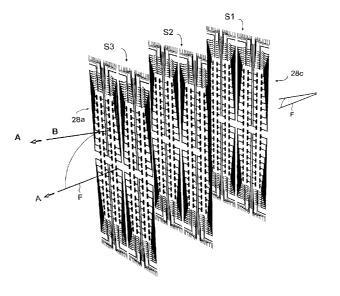
In the illustration of Figures 7a and 7b instead of each stage S 1-S3 having a
corresponding ring 10a-10c of PTs 14, PTs 14 are arranged in grids 28a, 28b
and 28c. In the
example illustrated, which is not intended to be limiting, each grid 28a-28c,
includes four
adjacent and co-planar rectangular grid quadrant arrangements of PTs 14 having
corresponding grid and pin addresses. So for example in the view of Figure 7a
the rectangular
grid quadrant in the upper left hand quadrant of grid 28a includes pin
addresses S1CC1:1-
S1CC1:9, and S1CC2:1-S1CC2:9. Each pin address has its corresponding PT 14
which, when
energized as in the example of Figure 3, ionizes the gas or other plasma fuel
in the
corresponding gap 16 so as to produce a plasma thrust in a direction
substantially
perpendicular to the plane, shown as plane E, containing grid 28a. Again it
will be understood
that the grids illustrated in Figures 7a and 7b are expanded for ease of
viewing, and would
most likely be much more compressed, and each of the stages Si-S3 would be
tightly packed
in a stack along axis F, wherein axis of symmetry F is orthogonal to plane E,
that is orthogonal
to the plane containing stage Sl.
14
CA 02827166 2013-09-12
The pins and corresponding PTs 14 in each grid in each quadrant of grid 28a
are sequentially energized in a progression which cycles around the grids in
each quadrant of
grid 28a and then switched to stage S2 and corresponding grid 28b, and when
the sequential
energizing in the same progression around the quadrants of grid 28b is
completed, the
sequential energizing of the PTs 14 is switched to grid 28c of stage S3, and
then looped back
to stage Si to continue the sequential energizing progression of all of the
PTs 14 so as to
thereby generate a continuous cumulative plasma drive thrust shown
diagrammatically by
direction arrow A. Alternatively, the sequencing algorithm may be altered to
change the
direction of the cumulative thrust, for example, as seen in Figure 7b, so as
to be directed in
direction A' along re-directed thrust axis B. Thus, for example if it was
designed to change
the direction of the thrust axis B, the concentration of PTs 14 being fired
may be increased
through the stages along thrust axis B in the desired direction of thrust A'.
In one experiment, timing of the relays was optimized resulting in a
noticeable
lowering of the power consumption. In the experiment, as the timing became
optimized the
power consumption of a circular array dropped from 14 W to 9 W. In the
experiment the
plasma source, that is, the source of resistance, was air. Sequentially
triggering of the relays in
the array resulted, for lack of a better expression, in a series of bursts of
energy 13. The series
of bursts could for example be used as a plasma turbine as described above for
the
arrangement rings of PTs in multiple sequentially triggered stages, where the
sequential
triggering of the relays (or plasma gates) for each array of PTs and the
sequential triggering of
each stage, is done at high speeds, using relatively little energy input and
no mechanical parts
(with the exception of the relay components in embodiments employing relays).
Using an alternating current power source the plasma resolution of the system
may be very tightly compressed, providing multiple PT resistance points
without having to
provide many corresponding ground locations. The use of plasma gates instead
of relays or
the use of hybrid plasma gates 30, wherein plasma gates are integrated as
shown with the
CA 02827166 2013-09-12
electrodes, increases the resolution, and potentially increasing the number of
PTs 14 per unit
area per stage.
In one experiment multiple relays were positioned around in a non-conductive
cylinder. The wires from the relays extended through the cylinder to a gap
between the
opposing side and the continuation of the electrical circuit. The gap was used
to create plasma
in the chamber.
A micro controller was programmed to throw the relays one after another, and
then release them. The program switched relays every 100 milli-seconds,
although this is not
intended to be limiting. The distance of the arc between the electrodes was
adjusted to
establish a functional optimized resistance.
It was found that, even though using AC power, there was an electrical
magnetic disturbance that affected the micro controller. Doing more research
applicant
developed a shielded relay which was protected from electrical energy. Because
of the size,
speed and function of a relay, a plasma gate switching system as described
below may work
better for a plasma drive application.
It was found that, by having the relays throw and hold (i.e. pause while
energized) for the same amount of time, a better connection resulted. This
allowed the use of
the original relays which then worked without as many of the problems being
caused by
electro magnetic disturbance. However, the shielded relays still however
worked better than
the unshielded ones. Also without shielding, the micro control program that
controlled the
operation of the relays was still affected by the electro magnetic
disturbance.
The relays were successfully operated at interval speeds of approximately four
milliseconds, where all plasma connections were operating. The power
consumption was
16
CA 02827166 2013-09-12
observed when using one plasma connection and a meter to observe the wattage.
The one
connection used 13 watts and when five plasma connections were tested, with
the relay
connections throwing at 6 milliseconds, the power consumption was reduced to 9
watts. Thus,
power savings of approximately 30 percent were obtained. It is anticipated
that semi-
conductor switches may also be used instead of relays.
As seen in Figure 8a, hybrid plasma gate 30 includes conductor 32 for
supplying alternating current or direct current power/ground to electrodes
34a. Plasma gate 36
is mounted behind, so as to cooperate with electrodes 34b. Electrodes 34a are
in opposed
facing relation to electrodes 34b across plasma arc gap 38. Plasma arc's 40
cross gap 38 so as
to energize selected electrodes 34b by operation of force generators 42.
Conductor 44 supplies
ac or de power/ground to plasma gate 36.
As seen in Figure 8b, a plasma drive stage Sn, may be formed by an integrated
side-by-side array of hybrid plasma gates 30. For the illustrated example
stage Sn contains
sixteen side-by-side hybrid plasma gates 30, aligned so that plasma gaps 38
for each hybrid
plasma gate 30 collectively from a plasma cavity 46 from which thrust may be
directed for
example in directions G, H, G' or H'. In Figure 8c two stages, Sn and Sn+1,
are overlapped
one on top of another. Both stages collectively produce thrust for example in
one of the
illustrated directions. Other embodiments (not shown) may employ more than two
overlapped
stages, and each stage may include a grid work of multiple arrays of hybrid
plasma gates 30.
Plasma Gate for Plasma Drive
The plasma gate described herein and illustrated in Figures 9-18 may be
characterized in one aspect as including at least one conductive input line
having a
corresponding at least one terminal end, a plurality of conductive output
lines having a
corresponding plurality of input ends, and a plasma gap having opposite first
and second ends,
where the plasma gap extends between the terminal ends of the input lines and
the input ends
17
CA 02827166 2013-09-12
of the output lines. A plasma-generating gas is resident in the plasma gap. At
least one field
generator having a field-generating distal end is mounted so as to position
the distal end of the
field generator adjacent the plasma gap. The output lines are arrayed along
the plasma gap in a
spaced apart array. The distal end of the field generator is positioned at
least at the first end of
the plasma gap.
In a preferred embodiment the plasma gap is elongate and may be
substantially linear, and wherein the input line is an array of input lines.
Consequently the at
least one teiminal end is a corresponding array of terminal ends con-esponding
to said array of
conductive input lines. The plurality of input ends correspond to, and are
substantially aligned
with, the array of terminal ends. In one embodiment the plasma gap has a
lateral width
dimension which is constant, and another embodiment where it is not constant.
For example
the plasma gap may diverge or converge. In the case where the at least one
field generator is a
single generator field positioned at a first end of the plasma gap, the plasma
gap may diverge
or converge so as to diverge or converge respectively from the first end to
the second end of
the plasma gap.
In a further embodiment the at least one field generator includes a pair of
field
generators in opposed facing relation at the opposite ends of the plasma gap.
The pair of field
generators may be substantially parallel.
Where the at least one conductive input line is an array of conductive input
lines, the at least one terminal end is a corresponding array of teiminal ends
corresponding to
the array of conductive input lines. Preferably the plurality of input ends
correspond to, and
are substantially aligned with, the array of terminal ends.
18
CA 02827166 2013-09-12
The plasma gap may be configured so that it has a center-line extending
substantially equidistant between the terminal ends and the input ends. In one
embodiment the
distal end of at least one field generator is angled relative to the gap
center-line. The distal end
may be offset from the center-line.
In a plasma gating method employing embodiments summarized above, the
method includes the steps of:
a) providing at least one conductive input line having a corresponding at
least one terminal end,
b) providing a plurality of conductive output lines having a corresponding
plurality of input ends,
c) providing a plasma gap having opposite first and second ends, the
plasma gap extending between the at least one terminal end and the
plurality of input ends, and providing a plasma-generating gas in the
plasma gap,
d) providing at least one field generator having a field-generating distal
end mounted so as to position the distal end adjacent the plasma gap,
wherein said plurality of conductive output lines are arrayed along the
plasma gap in a spaced apart array, and the distal end is positioned at
least at the first end of the plasma gap,
e) selectively creating a plasma arc across the plasma gap
from the at least
one terminal end to the plurality of input ends,
19
CA 02827166 2013-09-12
creating a field from the at least one field generator,
g) controlling the field so as to control a position of
the plasma arc.
As illustrated in Figures 9-18, for each plasma gate, junction 110, which may
for example appear on a circuit board as the junction illustrated in Figure
10a, includes at least
one electrically conductive input line 112, wherein each input line 112 has a
corresponding
terminal end 112a, a plurality of electrically conductive output lines 114,
each having a
corresponding input end 114a, and a field generator 116 having a distal end
116a positioned
adjacent a plasma gap 118 between terminal ends 112a and input ends 114a. Thus
a single or
multiple signal paths come into junction 110 on input line(s) 112, and by
selectively
positioning a plasma arc or bridge 120 across plasma gap 118, the signals are
directed to a
desired output path 114. Thus by selectively positioning the plasma arc
bridging across gap
118 by the use of field generator 116, discreet input lines 112 as applicable
and discreet output
lines 114 may be selected for any particular signal. The temi signal as used
herein is intended
to mean, and without intending to be limiting, electrical power and
correspondingly
transmitted data, whether analog or digital. As uses herein the teiiii digital
data is not intended
to be restricted to binary data.
Testing was initially done in an electron chamber using a neon gas as the
plasma gas within the chamber and using an alternating current power source.
Experimentation was also done using a direct current power source and using
ambient air
instead of neon gas. Further experiments confirmed that data from a micro
controller (not
shown) could be sent and received across a plasma gate substantially as
described herein.
Thus for example in Figure 13, an elongate, pointed, electrically conductive
object, such as a
metal nail or spike was successfully employed as a field generator 116. Field
generator 116
was positively charged, and in the experiment of Figure 13, the distal end
116a of the field
CA 02827166 2013-09-12
generator was angled so that the point was off to the side of plasma gap 118,
that is, offset
laterally relative to a centroidal axis AA, wherein axis AA is substantially
centroidally aligned
along and through plasma gap 118. Plasma gap 118 runs between an opposed-
facing pair of
substantially parallel arrays of electrical connection points.
With respect to the embodiments of Figures 9-13, which not intended to be
limiting, with field generator 116 positioned to place distal end 116a
adjacent one end of
plasma gap 118, producing a negative field from field generator 116 repulses
or otherwise
causes to move away plasma arc or bridge 120, shown by way of example in
dotted outline in
Figure 9, from the negative field of the field generator.
It was found advantageous in controlling multiple connections through one
junction point to have the positive circuit, for example input line 112, have
multiple
connection points at ends 112a so as to match the opposing negative electrical
connections of
ends 114a across plasma gap 118. Proper spacing of ends 112a from ends 114a,
that is, the
spacing between the negative and the positive electrical connections on each
side of plasma
gap 118, was adjusted so that only one plasma bridge 120 crossed gap 118 when
the circuit
was energized. The positioning of plasma bridge 120 was accomplished using
either a
negative or a positive field from field generator 116. Thus when a negative
field was
generated, the plasma bridge 120 moved away from the negative field generator.
With the
field turned off the position of the plasma bridge (or arc) 120 was stable and
did not move
along gap 118. Although not intended to be limited to any particular theory of
operation, it is
postulated that in this instance the resistance in the first electrical
connection has been
increased so that the plasma bridge 120 will move to the next path of least
resistance in a
direction away from the field generator. Conversely, the use of a positive
field from field
generator 116, attracts plasma bridge 120 so as to connect to an electrical
connection closer to
field generator 116. Thus manipulating the polarity and strength of the field
from field
CA 02827166 2013-09-12
generator 116, allows the controlled switching of plasma bridge 120 along the
array or arrays
of electrical connections along plasma gap 118.
In the embodiment of Figure 11, the lateral spacing between ends 112a and
ends 114a is increased, that is plasma gap 118 diverges as the distance
increases from field
generator 116 along plasma gap 118. This makes a variable distance between the
positive and
negative connection points across plasma gap 118. Plasma gap 118 diverges in
Figure 11 and
converges in Figure 8, although this is not intended to be limited. Using the
configurations of
Figures 2 or 8 it is postulated that the position of plasma bridge 120 may be
better controlled
because the current will go to the closest spaced connection, because of the
least resistance,
until a field from field generator 116 pushes plasma bridge 120 away or pulls
bridge 120
towards field generator 116 so as to move bridge 120 further away along the
arrays of
connection points or closer in along the arrays of connection points. However,
when no field
is being generated by field generator 116, plasma bridge 120 will return to
its original position
between the laterally closest spaced connection points on ends 112a and 114a,
that is, which
are closest to each other across plasma gap 118. Thus in the illustration of
Figure 11, which is
not intended to be limiting, the return or original position of plasma bridge
120 is the opposed-
facing pair of connection points closest to field generator 116. In Figure 18
it is the pair of
connection points furthest from field generator 116.
In the embodiment of Figure 12, an opposed-facing, aligned pair of field
generators 116 are positioned on centroidal axis AA, with their corresponding
distal ends 116a
directed into plasma gap 118. It is postulated that this results in more
control of the circuit
switching as the stability of the position of plasma bride 120 along plasma
gap 118 may be
improved so that the connected circuits may be stably held in place and when
desired moved
along plasma gap 118 with a stationary power factor.
CA 02827166 2013-09-12
With respect to Figure 13, in testing it was found that the angled side of
distal
end 116a of field generator 116 had a different polarity or otherwise was
different as compared
to the arrangements of field generator 116 shown in Figures 9-12. The angling
of distal end
116a towards inputs 114a of outputs 114 was found to be more effective for
changing the
circuits, as switching the circuits through the various input and output lines
112 and 114
respectively, which were mounted on non-conductive base 18, was accomplished
with greater
ease. The offset point 116a of field generator 116 was aimed at inputs 114a so
as to "push" or
urge the plasma arc 120 where it needed to go, i.e., from outputs 112a to
inputs 114a, thereby
using less power and establishing the plasma arc 120 more quickly.
Systems such as seen in Figures 15a, 15b and 16 may be employed for
switching by first junctions 10 amongst further arrays of junctions 10. Thus
as seen in Figure
15a, a first junction 110a, which is a version of the junction of Figure 12
although this is not
intending to be limiting, controls output to second junctions 110b, 110c, and
110d. Second
junctions 110b, 110c and 110d themselves are each versions of the junction 120
of Figure 12,
although again this is not intended to be limiting as other junctions 110 will
also work as is the
case with junction 110a. Thus second junctions 110b, 110c, and 110d each
switch their
circuits (circuits inputs 112 and corresponding outputs 114) as controlled by
their
corresponding field generators 116. As will be understood, the outputs 114
from junction
110a may go to a lesser or greater number of second junctions being switched.
As seen in Figure 15b, first junction 110e directs its outputs 114 not to the
inputs 112 of second junctions 110f-110h, but to the inputs of the field
generators 116
corresponding to second junctions 110f-110h. In the embodiment of Figure 15b
the output of
junction 110e will, depending on the switch path closed by the operation of
the field
generators of junction 110e, control the switch path which is closed in the
corresponding
second junction 110f, 110g, or 110h. Pairs of output lines from junction 110e
lead to
corresponding single second junctions, that is, either to junction 110f, 110g
or 110h. Each pair
CA 02827166 2013-09-12
of output lines splits so that each output line of the pair powers or
otherwise controls the field
generated by a corresponding field generator from the opposed-facing pair of
field generators
on each of junctions 110f, 110g and 110h which control the circuits for a
regulated power
source 124. Thus it will be appreciated that at any one time, only the field
generator on one
side or the other of junctions 110f, 110g and 110h will be powered. Because
power is supplied
by power source 124 to all three of second junctions 110f, 110g, 110h, while
the field
generators for any one of these three second junctions is controlling/moving
the position of the
corresponding plasma arc 120, the plasma arcs in the other two second
junctions remain stable
and live. It will be understood that more than three second junctions may be
employed.
Figure 15b may be used for counting plus or minus, i.e., counting up or down
(1, 2, etc.) as the circuits sub-divide into time sequences.
In Figure 16 an array of the junction 110 circuits of Figure 15b are provided
to
show how the sub-divided, sequences may be employed. It is understood that one
or more
=
arrays of junctions 110 may be arranged concentrically outwardly (in a
functional sense) of the
illustrated array so that each output 114 branches to its own further junction
110 and so on
creating a network of junctions.
If such a network was to form a building block of for example a digital
processor or plasma drive, the sequence of inter-related connections within
the network could
be programmed, and if any one sequence became damaged for example, then the
sequence
could be re-routed without the damage impairing the functioning of the
network. It is
understood that the arrays of junctions 110 could network in three dimensions,
and that gaps
118 could thus be two-dimensional gaps between a planar or other two-
dimensional array of
inputs 112 and a spaced apart, opposed-facing two-dimensional array of outputs
114.
24
CA 02827166 2013-09-12
The plasma gate could be configured as a counting/time/hertz rate system such
as seen in Figures 17 and 18. This could be done by using an energy bursting-
type device 122
such as a capacitor that stores energy and then releases a burst of energy
into the field
generator 116, which may in one embodiment as seen in Figure 18 be a coil-
shaped field
generator 116b. This energy could be controlled by means of using one of its
own circuits or it
could be energized by a different line or controlled by a separate device.
This could be set up
so that one burst would energize all the circuits, i.e. all of the individual
input lines 112 and
output lines 114, in a numerical sequence sequentially, that is, one at a
time, and then return to
the first circuit (i.e., the first input line 112' and corresponding first
output line 114')
representing zero. In Figure 17a, energy bursting device 122 energizes a
pointed field
generator 116 such as used in the embodiment of Figure 9. In Figure 17b the
energy bursting
device 122 is charging when the closed circuit is between input 112' and
output 114' as
illustrated. Once device 122 is charged and releases its energy as a burst,
plasma arc 120 is
pushed away from filed generator 116, sequentially closing the circuits along
plasma gap 118
in direction of the diverging of plasma gap 118. Once the energy has dispersed
from device
122, the plasma arc 120 returns to its position 112'. 114' closest to field
generator 116 while
device 122 again charges. The cycle repeats with a frequency which depends on
the charge
time and pulse time of device 122 and the response time for the plasma arc to
return to the
home position at 112', 114'. As seen in Figure 18, advantageously a converging
plasma gap
118 may be employed in conjunction with energy burst device 122 and its
associated field
generator 116b, as applicant has observed that a coil-shaped field generator
is better at
"pulling" plasma arc 120 towards the coil 116b than "pushing" plasma arc away
from the coil
116b.
Of relevance to the present invention are the results of testing of a junction
110
using direct current in the presence of neon gas, wherein the neon gas and
junction circuits
were contained within a sealed vessel. The sealed vessel was breached with a
hair-line crack
allowing the escape of some of the neon gas and a small quantity of ambient
air into the vessel,
CA 02827166 2013-09-12
and in particular into the plasma gap. From the appearance of the plasma arc
across the
plasma gap it appeared to applicant that the mixed gas (ambient air mixed with
neon gas)
worked better. The line of the plasma arc became more pronounced and thinner.
Applicant
consequently surmises that this would likely allow for the voltage to be
reduced to still
produce a useful plasma arc.
With respect to the use of magnets 126, seen in Figure 13, they are
illustrated
as merely one example of a means for controlling or lowering the voltage at
the field
generator. Other means for controlling or lowering the voltage may include
coils, capacitors,
etc., which then provide for more controlled switching amongst the circuits of
junction 110.
As will be apparent to those skilled in the art in the light of the foregoing
disclosure, many alterations and modifications are possible in the practice of
this invention
without departing from the spirit or scope thereof. Accordingly, the scope of
the invention is
to be construed in accordance with the substance defined by the following
claims.
26