Note: Descriptions are shown in the official language in which they were submitted.
CA 02827632 2013-08-16
WO 2012/161773
PCT/US2012/025916
ORGANIC PHOTOVOLTAIC CELL INCORPORATING
ELECTRON CONDUCTING EXCITON BLOCKING LAYERS
Cross-Reference to Related Application
[001] This application claims the benefit of priority to U.S. Provisional
Application
No. 61/444,899, filed on February 21, 2011, and U.S. Provisional Application
No.
61/479,237, filed on April 26, 2011, both of which are incorporated herein by
reference in
their entireties.
Statement Regarding Federally Sponsored Research
[002] This invention was made with U.S. Government support under DE-
5C00000957 and DE-5C0001013, both awarded by the U.S. Department of Energy.
The
government has certain rights in the invention.
Joint Research Agreement
[003] The claimed invention was made by, on behalf of, and/or in connection
with
one or more of the following parties to a joint university-corporation
research agreement:
University of Michigan, and Global Photonic Energy Corporation. The agreement
was in
effect on and before the date the invention was made, and the claimed
invention was made as
a result of activities undertaken within the scope of the agreement.
Field of the Disclosure
[004] The present disclosure generally relates to photosensitive
optoelectronic
devices comprising at least one blocking layer, such as electron conducting,
exciton blocking
layers. The present disclosure also relates to methods of increasing power
conversion
efficiency in photosensitive optoelectronic devices using at least one the
blocking layers
described herein. The electron conducting, exciton blocking layers of the
devices presently
disclosed may provide for improved performance characteristics, such as
increased open
circuit voltage, short circuit current, fill factor, or power conversion
efficiency.
1
CA 02827632 2013-08-16
WO 2012/161773
PCT/US2012/025916
Background
[005] Optoelectronic devices rely on the optical and electronic properties of
materials to either produce or detect electromagnetic radiation electronically
or to generate
electricity from ambient electromagnetic radiation.
[006] Photosensitive optoelectronic devices convert electromagnetic radiation
into
electricity. Solar cells, also called photovoltaic (PV) devices, are a type of
photosensitive
optoelectronic device that is specifically used to generate electrical power.
PV devices,
which may generate electrical energy from light sources other than sunlight,
can be used to
drive power consuming loads to provide, for example, lighting, heating, or to
power
electronic circuitry or devices such as calculators, radios, computers or
remote monitoring or
communications equipment. These power generation applications also often
involve the
charging of batteries or other energy storage devices so that operation may
continue when
direct illumination from the sun or other light sources is not available, or
to balance the
power output of the PV device with a specific application's requirements. As
used herein the
term "resistive load" refers to any power consuming or storing circuit,
device, equipment or
system.
[007] Another type of photosensitive optoelectronic device is a photoconductor
cell.
In this function, signal detection circuitry monitors the resistance of the
device to detect
changes due to the absorption of light.
[008] Another type of photosensitive optoelectronic device is a photodetector.
In
operation a photodetector is used in conjunction with a current detecting
circuit which
measures the current generated when the photodetector is exposed to
electromagnetic
radiation and may have an applied bias voltage. A detecting circuit as
described herein is
capable of providing a bias voltage to a photodetector and measuring the
electronic response
of the photodetector to electromagnetic radiation.
- 2 -
CA 02827632 2013-08-16
WO 2012/161773
PCT/US2012/025916
[009] These three classes of photosensitive optoelectronic devices may be
characterized according to whether a rectifying junction as defined below is
present and also
according to whether the device is operated with an external applied voltage,
also known as a
bias or bias voltage. A photoconductor cell does not have a rectifying
junction and is
normally operated with a bias. A PV device has at least one rectifying
junction and is
operated with no bias. A photodetector has at least one rectifying junction
and is usually but
not always operated with a bias. As a general rule, a photovoltaic cell
provides power to a
circuit, device or equipment, but does not provide a signal or current to
control detection
circuitry, or the output of information from the detection circuitry. In
contrast, a
photodetector or photoconductor provides a signal or current to control
detection circuitry, or
the output of information from the detection circuitry but does not provide
power to the
circuitry, device or equipment.
[010] Traditionally, photosensitive optoelectronic devices have been
constructed of
a number of inorganic semiconductors, e.g., crystalline, polycrystalline and
amorphous
silicon, gallium arsenide, cadmium telluride and others. Herein the term
"semiconductor"
denotes materials which can conduct electricity when charge carriers are
induced by thermal
or electromagnetic excitation. The term "photoconductive" generally relates to
the process in
which electromagnetic radiant energy is absorbed and thereby converted to
excitation energy
of electric charge carriers so that the carriers can conduct, L e., transport,
electric charge in a
material. The terms "photoconductor" and "photoconductive material" are used
herein to
refer to semiconductor materials which are chosen for their property of
absorbing
electromagnetic radiation to generate electric charge carriers.
[011] PV devices may be characterized by the efficiency with which they can
convert incident solar power to useful electric power. Devices utilizing
crystalline or
amorphous silicon dominate commercial applications, and some have achieved
efficiencies of
- 3 -
CA 02827632 2013-08-16
WO 2012/161773
PCT/US2012/025916
23% or greater. However, efficient crystalline-based devices, especially of
large surface area,
are difficult and expensive to produce due to the problems inherent in
producing large
crystals without significant efficiency-degrading defects. On the other hand,
high efficiency
amorphous silicon devices still suffer from problems with stability. Present
commercially
available amorphous silicon cells have stabilized efficiencies between 4 and
8%. More recent
efforts have focused on the use of organic photovoltaic cells to achieve
acceptable
photovoltaic conversion efficiencies with economical production costs.
[012] PV devices may be optimized for maximum electrical power generation
under
standard illumination conditions (i.e., Standard Test Conditions which are
1000 W/m2,
AM1.5 spectral illumination), for the maximum product of photocurrent times
photovoltage.
The power conversion efficiency of such a cell under standard illumination
conditions
depends on the following three parameters: (1) the current under zero bias,
i.e., the short-
circuit current /sc, in Amperes (2) the photovoltage under open circuit
conditions, i.e., the
open circuit voltage Voc, in Volts and (3) the fill factor, FF.
[013] PV devices produce a photo-generated current when they are connected
across
a load and are irradiated by light. When irradiated under infinite load, a PV
device generates
its maximum possible voltage, V open-circuit, or Voc. When irradiated with its
electrical
contacts shorted, a PV device generates its maximum possible current, I short-
circuit, or 'sc.
When actually used to generate power, a PV device is connected to a finite
resistive load and
the power output is given by the product of the current and voltage, I xV. The
maximum
total power generated by a PV device is inherently incapable of exceeding the
product, 'Sc x
Voc. When the load value is optimized for maximum power extraction, the
current and
voltage have the values, 'max and Vmax, respectively.
[014] A figure of merit for PV devices is the fill factor, FF , defined as:
FF = 11,,,axV .11 {IscV oc } (1)
- 4 -
CA 02827632 2013-08-16
WO 2012/161773
PCT/US2012/025916
where FF is always less than 1, as 'Sc and Voc are never obtained
simultaneously in actual
use. Nonetheless, as FF approaches 1, the device has less series or internal
resistance and
thus delivers a greater percentage of the product of Isc and Voc to the load
under optimal
conditions. Where Pine is the power incident on a device, the power efficiency
of the device,
may be calculated by:
lip = FF * (Isc* Voc) I Pine
[015] When electromagnetic radiation of an appropriate energy is incident upon
a
semiconductive organic material, for example, an organic molecular crystal
(OMC) material,
or a polymer, a photon can be absorbed to produce an excited molecular state.
This is
represented symbolically as So + hv tP So*. Here So and So* denote ground and
excited
molecular states, respectively. This energy absorption is associated with the
promotion of an
electron from a bound state in the highest occupied molecular orbital (HOMO)
energy level,
which may be a B-bond, to the lowest unoccupied molecular orbital (LUMO)
energy level,
which may be a B*-bond, or equivalently, the promotion of a hole from the LUMO
energy
level to the HOMO energy level. In organic thin-film photoconductors, the
generated
molecular state is generally believed to be an exciton, i.e., an electron-hole
pair in a bound
state which is transported as a quasi-particle. The excitons can have an
appreciable life-time
before geminate recombination, which refers to the process of the original
electron and hole
recombining with each other, as opposed to recombination with holes or
electrons from other
pairs. To produce a photocurrent the electron-hole pair becomes separated,
typically at a
donor-acceptor interface between two dissimilar contacting organic thin films.
If the charges
do not separate, they can recombine in a geminant recombination process, also
known as
quenching, either radiatively, by the emission of light of a lower energy than
the incident
light, or non-radiatively, by the production of heat. Either of these outcomes
is undesirable in
a photosensitive optoelectronic device.
- 5 -
CA 02827632 2013-08-16
WO 2012/161773
PCT/US2012/025916
[016] Electric fields or inhomogeneities at a contact may cause an exciton to
quench
rather than dissociate at the donor-acceptor interface, resulting in no net
contribution to the
current. Therefore, it is desirable to keep photogenerated excitons away from
the contacts.
This has the effect of limiting the diffusion of excitons to the region near
the junction so that
the associated electric field has an increased opportunity to separate charge
carriers liberated
by the dissociation of the excitons near the junction.
[017] To produce internally generated electric fields which occupy a
substantial
volume, the usual method is to juxtapose two layers of material with
appropriately selected
conductive properties, especially with respect to their distribution of
molecular quantum
energy states. The interface of these two materials is called a photovoltaic
heterojunction. In
traditional semiconductor theory, materials for forming PV heterojunctions
have been
denoted as generally being of either n or p type. Here n-type denotes that the
majority carrier
type is the electron. This could be viewed as the material having many
electrons in relatively
free energy states. The p-type denotes that the majority carrier type is the
hole. Such
material has many holes in relatively free energy states. The type of the
background, i.e., not
photo-generated, majority carrier concentration depends primarily on
unintentional doping by
defects or impurities. The type and concentration of impurities determine the
value of the
Fermi energy, or level, within the gap between the highest occupied molecular
orbital
(HOMO) energy level and the lowest unoccupied molecular orbital (LUMO) energy
level,
called the HOMO-LUMO gap. The Fermi energy characterizes the statistical
occupation of
molecular quantum energy states denoted by the value of energy for which the
probability of
occupation is equal to 1/2. A Fermi energy near the LUMO energy level
indicates that
electrons are the predominant carrier. A Fermi energy near the HOMO energy
level indicates
that holes are the predominant carrier. Accordingly, the Fermi energy is a
primary
- 6 -
CA 02827632 2013-08-16
WO 2012/161773
PCT/US2012/025916
characterizing property of traditional semiconductors and the prototypical PV
heterojunction
has traditionally been the p-n interface.
[018] The term "rectifying" denotes, inter alia, that an interface has an
asymmetric
conduction characteristic, i.e., the interface supports electronic charge
transport preferably in
one direction. Rectification is associated normally with a built-in electric
field which occurs
at the heterojunction between appropriately selected materials.
[019] As used herein, and as would be generally understood by one skilled in
the art,
a first "Highest Occupied Molecular Orbital" (HOMO) or "Lowest Unoccupied
Molecular
Orbital" (LUMO) energy level is "greater than" or "higher than" a second HOMO
or LUMO
energy level if the first energy level is closer to the vacuum energy level.
Since ionization
potentials (IP) are measured as a negative energy relative to a vacuum level,
a higher HOMO
energy level corresponds to an IP having a smaller absolute value (an IP that
is less negative).
Similarly, a higher LUMO energy level corresponds to an electron affinity (EA)
having a
smaller absolute value (an EA that is less negative). On a conventional energy
level diagram,
with the vacuum level at the top, the LUMO energy level of a material is
higher than the
HOMO energy level of the same material. A "higher" HOMO or LUMO energy level
appears closer to the top of such a diagram than a "lower" HOMO or LUMO energy
level.
[020] In the context of organic materials, the terms "donor" and "acceptor"
refer to
the relative positions of the HOMO and LUMO energy levels of two contacting
but different
organic materials. This is in contrast to the use of these terms in the
inorganic context, where
"donor" and "acceptor" may refer to types of dopants that may be used to
create inorganic n-
and p- types layers, respectively. In the organic context, if the LUMO energy
level of one
material in contact with another is lower, then that material is an acceptor.
Otherwise it is a
donor. It is energetically favorable, in the absence of an external bias, for
electrons at a
- 7 -
CA 02827632 2013-08-16
WO 2012/161773
PCT/US2012/025916
donor-acceptor junction to move into the acceptor material, and for holes to
move into the
donor material.
[021] A significant property in organic semiconductors is carrier mobility.
Mobility
measures the ease with which a charge carrier can move through a conducting
material in
response to an electric field. In the context of organic photosensitive
devices, a layer
including a material that conducts preferentially by electrons due to a high
electron mobility
may be referred to as an electron transport layer, or ETL. A layer including a
material that
conducts preferentially by holes due to a high hole mobility may be referred
to as a hole
transport layer, or HTL. Preferably, but not necessarily, an acceptor material
is an ETL and a
donor material is a HTL.
[022] Conventional inorganic semiconductor PV cells employ a p-n junction to
establish an internal field. Early organic thin film cell, such as reported by
Tang, AppL Phys
Lett. 48, 183 (1986), contain a heterojunction analogous to that employed in a
conventional
inorganic PV cell. However, it is now recognized that in addition to the
establishment of a p-
n type junction, the energy level offset of the heterojunction also plays an
important role.
[023] The energy level offset at the organic D-A heterojunction is believed to
be
important to the operation of organic PV devices due to the fundamental nature
of the
photogeneration process in organic materials. Upon optical excitation of an
organic material,
localized Frenkel or charge-transfer excitons are generated. For electrical
detection or current
generation to occur, the bound excitons must be dissociated into their
constituent electrons
and holes. Such a process can be induced by the built-in electric field, but
the efficiency at
the electric fields typically found in organic devices (F ¨ 106 V/cm) is low.
The most
efficient exciton dissociation in organic materials occurs at a donor-acceptor
(D-A) interface.
At such an interface, the donor material with a low ionization potential forms
a
heterojunction with an acceptor material with a high electron affinity.
Depending on the
- 8 -
CA 02827632 2013-08-16
WO 2012/161773
PCT/US2012/025916
alignment of the energy levels of the donor and acceptor materials, the
dissociation of the
exciton can become energetically favorable at such an interface, leading to a
free electron
polaron in the acceptor material and a free hole polaron in the donor
material.
[024] Organic PV cells have many potential advantages when compared to
traditional silicon-based devices. Organic PV cells are light weight,
economical in materials
use, and can be deposited on low cost substrates, such as flexible plastic
foils. However,
organic PV devices typically have relatively low external quantum efficiency
(electromagnetic radiation to electricity conversion efficiency), being on the
order of 1 % or
less. This is, in part, thought to be due to the second order nature of the
intrinsic
photoconductive process. That is, carrier generation requires exciton
generation, diffusion
and ionization or collection. There is an efficiency qassociated with each of
these processes.
Subscripts may be used as follows: P for power efficiency, EXT for external
quantum
efficiency, A for photon absorption, ED for diffusion, CC for collection, and
INT for internal
quantum efficiency. Using this notation:
11p ¨11ExT ¨11A *11ED *11cc
11ExT ¨11A *111NT
[025] The diffusion length (LD) of an exciton is typically much less (LD ¨ 5
nm) than
the optical absorption length (-50 nm), requiring a trade-off between using a
thick layer
where generated excitons are too distant to be dissociated at the
heterojunction, or a thin cell
with a low optical absorption efficiency.
= J
sc
[026] The power conversion efficiency may be expressed as 7 7 , = V oc = FF
,
Po
where Voc is the open circuit voltage, FF is the fill factor, J:õ is the short
circuit current, and
Po is the input optical power. One way to improve tip is through the
enhancement of V,,
- 9 -
CA 02827632 2013-08-16
WO 2012/161773
PCT/US2012/025916
which is still 3-4 times less than the typical absorbed photon energy in most
organic PV cells.
The relationship between dark current and Võ may be inferred from:
(V ¨ J R s) V
exp q 1+ ¨} (1)
Rs + Rp nkT
where J is the total current, J, is the reverse dark saturation current, n is
the ideality factor, Rs
is the series resistance, Rp is the parallel resistance, V is the bias
voltage, and Jph is the
photocurrent (Rand et al., Phys. Rev. B, vol. 75, 115327 (2007)). Setting J=0:
T T
kT C V
Voc n- O+1 oc (2)
q R J
p z
when Jph/J, >> 1, Voc is proportional to In(Jph/Js), suggesting that a large
dark current, Js,
results in a reduction in Voc.
[027] Exciton blocking layers that also function as electron blocking layers
have
been developed for polymer Bulk Heterojunction (BHJ) PV cells (Hams et al.,
AppL Phys.
Lett., vol. 92, 023504 (2008)). In polymer BHJ PV cells, blended polymers of
donor and
acceptor materials are used as the active region. These blends can have
regions of donor or
acceptor material extending from one electrode to the other. Therefore, there
can be electron
or hole conduction pathways between the electrodes through one type of polymer
molecule.
[028] Besides polymer BHJ PV cells, other architectures, including planar
PV
devices, also exhibit a significant electron or hole leakage current across
the donor/acceptor
heterojunction when AF L or AFH is small, even though these films may not have
single
material (donor or acceptor) pathways between the two electrodes.
[029] The present disclosure relates to photosensitive optoelectronic
devices
comprising a compound blocking layer located between an acceptor material and
a cathode,
the compound blocking layer comprising: at least one electron conducting
material, and at
least one wide-gap electron conducting exciton blocking layer. This
combination of
- 10 -
CA 02827632 2013-08-16
WO 2012/161773
PCT/US2012/025916
materials serve as efficient electron conductors, leading to an improved fill
factor and
increased power conversion efficiency, compared to an analogous device using a
conventional blocking layers.
Summary of the Disclosure
[030] There is disclosed an organic photosensitive optoelectronic device
comprising: two electrodes comprising an anode and a cathode in superposed
relation; at least
one donor material and at least one acceptor material, wherein the donor
material and the
acceptor material form a photo-active region between the two electrodes; and a
compound
blocking layer located between the acceptor material and the cathode.
[031] In one embodiment, the compound blocking layer comprises: at least one
electron conducting material, and wide-gap electron conducting exciton
blocking layer.
[032] In another embodiment, the at least one acceptor material has a
lowest
unoccupied molecular orbital energy (LUMO-1) and the at least one electron
conducting
exciton blocking layer has a lowest unoccupied molecular orbital energy (LUMO-
2), wherein
LUMO-1 and LUMO-2 are aligned to permit electron transport directly from the
acceptor
material to the cathode. As used herein, LUMO levels aligned to permit
transport directly
from the acceptor material to the cathode means having an energy gap between
the first
lowest unoccupied molecular orbital energy and the second lowest unoccupied
molecular
orbital energy no greater than 0.5 eV, such as no greater than 0.3 eV, or even
less than 0.2
eV.
[033] In one embodiment, the at least one donor material is chosen from
squarine
(SQ), boron subphthalocyanonine chloride (SubPc), copper phthalocyanine
(CuPc), chloro-
aluminum phthalocyanine (C1A1Pc), poly(3-hexylthiophene) (P3HT), tin
phthalocyanine
(SnPc), pentacene, tetracene, diindenoperylene (DIP), and combinations thereof
-11-
CA 02827632 2013-08-16
WO 2012/161773
PCT/US2012/025916
[034] The at least one acceptor material is chosen from C60, C70
fullerenes,
3,4,9,10-perylenetetracarboxylic dianhydride (PTCDA), perfluorinated copper
phthalocyanine (F16-CuPc), PCBM, PC70BM, and combinations thereof
[035] In one embodiment, the at least one electron conducting material
comprises
3,4,9,10 perylenetetracarboxylic bisbenzimidazole (PTCBI).
[036] In another embodiment, the at least one wide-gap electron conducting
exciton blocking layer comprises 1,4,5,8-napthalene-tetracarboxylic-
dianhydride (NTCDA).
[037] Another embodiment used the combination of one electron conducting
material comprising 3,4,9,10 perylenetetracarboxylic bisbenzimidazole (PTCBI),
and at least
one wide-gap electron conducting exciton blocking layer comprising 1,4,5,8-
napthalene-
tetracarboxylic-dianhydride (NTCDA).
[038] The various layers disclosed herein have thicknesses the compound
blocking
layer has a thickness ranging from 10-100 nm, with the at least one electron
conducting
material ranging from 2-10 nm and the at least one wide-gap electron
conducting exciton
blocking layer ranging from 5-100 nm.
[039] It is appreciated that the organic photosensitive optoelectronic
device is an
organic photodetector, such as an organic solar cell. In one embodiment, the
organic solar
cell exhibits at least one of the following properties:
- a fill factor greater than 0.62,
- a spectrally corrected power conversion efficiency of at least 5.0% under
1 sun,
AM1.5G illumination, or
- a short circuit current of at least 7.5 mA/cm2.
[040] In one embodiment, the least one electrode may comprise transparent
conducting oxides, thin metal layers, or transparent conducting polymers. Non-
limiting
examples of the conducting oxides include indium tin oxide (ITO), tin oxide
(TO), gallium
- 12 -
CA 02827632 2013-08-16
WO 2012/161773
PCT/US2012/025916
indium tin oxide (GITO), zinc oxide (ZO), and zinc indium tin oxide (ZITO),
thin metal
layers are comprised of Ag, Al, Au or combinations thereof, and the
transparent conductive
polymers comprise polyanaline (PANT) and 3,4-
polyethylenedioxythiophene:polystyrenesulfonate (PEDOT:PSS).
[041] Non-limiting examples of the at least one electrode include a metal
substitute,
a non-metallic material or a metallic material chosen from Ag, Au, Ti, Sn, and
Al.
[042] In one embodiment, the at least one donor material comprises squarine,
the at
least one acceptor material comprises C60, the at least one electron
conducting material
comprises 3,4,9,10 perylenetetracarboxylic bisbenzimidazole (PTCBI), and the
at least one
wide-gap electron conducting exciton blocking layer comprises 1,4,5,8-
napthalene-
tetracarboxylic-dianhydride (NTCDA).
[043] There is also disclosed a method of making an organic photosensitive
optoelectronic device, the method comprising depositing onto a substrate at
least one
electrode comprising an anode and a cathode in superposed relation; at least
one donor
material and at least one acceptor material, wherein the donor material and
the acceptor
material form a photo-active region between the two electrodes; and depositing
a compound
blocking layer between the acceptor material and the cathode, the compound
blocking layer
comprising: at least one electron conducting material, and at least one wide-
gap electron
conducting exciton blocking layer.
[044] In another embodiment, the method comprises depositing the disclosed
materials, such as the at least one acceptor material having a lowest
unoccupied molecular
orbital energy (LUMO-1) and the at least one electron conducting exciton
blocking layer
having a lowest unoccupied molecular orbital energy (LUMO-2), wherein LUMO-1
and
LUMO-2 are aligned to permit electron transport directly from the acceptor
material to the
cathode.
- 13 -
CA 02827632 2013-08-16
WO 2012/161773
PCT/US2012/025916
[045] In one embodiment, the at least one donor material used in the
disclosed
method is chosen from squarine (SQ), boron subphthalocyanonine chloride
(SubPc), copper
phthalocyanine (CuPc), chloro-aluminum phthalocyanine (C1A1Pc), poly(3-
hexylthiophene)
(P3HT), tin phthalocyanine (SnPc), pentacene, tetracene, diindenoperylene
(DIP), and
combinations thereof
[046] The at least one acceptor material used in the disclosed method is
chosen
from C60, C70 fullerenes, 3,4,9,10-perylenetetracarboxylic dianhydride
(PTCDA),
perfluorinated copper phthalocyanine (F16-CuPc), PCBM, PC70BM, and
combinations
thereof
[047] In one embodiment, at least one electron conducting material used in
the
disclosed method comprises 3,4,9,10 perylenetetracarboxylic bisbenzimidazole
(PTCBI).
[048] In another embodiment, the at least one wide-gap electron conducting
exciton blocking layer used in the disclosed method comprises 1,4,5,8-
napthalene-
tetracarboxylic-dianhydride (NTCDA).
[049] Another embodiment of the disclosed method uses the combination of one
electron conducting material, such as 3,4,9,10 perylenetetracarboxylic
bisbenzimidazole
(PTCBI), and at least one wide-gap electron conducting exciton blocking layer,
such as
1,4,5,8-napthalene-tetracarboxylic-dianhydride (NTCDA).
[050] The method disclosed herein comprises depositing layers having
various
thicknesses, such as a compound blocking layer having a thickness ranging from
10-100 nm,
with the at least one electron conducting material ranging from 2-10 nm and
the at least one
wide-gap electron conducting exciton blocking layer ranging from 5-100 nm.
[051] The disclosed method also comprises depositing at the least one
electrode
that may comprise transparent conducting oxides, thin metal layers, or
transparent conducting
polymers. Non-limiting examples of the conducting oxides include indium tin
oxide (ITO),
- 14 -
CA 02827632 2013-08-16
WO 2012/161773
PCT/US2012/025916
tin oxide (TO), gallium indium tin oxide (GITO), zinc oxide (ZO), and zinc
indium tin oxide
(ZITO), thin metal layers are comprised of Ag, Al, Au or combinations thereof,
and the
transparent conductive polymers comprise polyanaline (PANT) and 3,4-
polyethylenedioxythiophene:polystyrenesulfonate (PEDOT:PSS).
[052] Non-limiting examples of the at least one electrode include a metal
substitute,
a non-metallic material or a metallic material chosen from Ag, Au, Ti, Sn, and
Al.
[053] In one embodiment, the method comprises deposition at least one donor
material comprising squarine, at least one acceptor material comprising C60,
at least one
electron conducting material comprising 3,4,9,10 perylenetetracarboxylic
bisbenzimidazole
(PTCBI), and at least one wide-gap electron conducting exciton blocking layer
comprising
1,4,5,8-napthalene-tetracarboxylic-dianhydride (NTCDA).
[054] The present disclosure is further directed to a method of increasing
the power
conversion efficiency of a photosensitive optoelectronic device comprising
incorporating the
compound blocking layer into the device.
[055] Aside from the subject matter discussed above, the present disclosure
includes
a number of other exemplary features such as those explained hereinafter. It
is to be
understood that both the foregoing description and the following description
are exemplary
only.
Brief Description of the Drawings
[056] The accompanying figures are incorporated in, and constitute a part of,
this
specification.
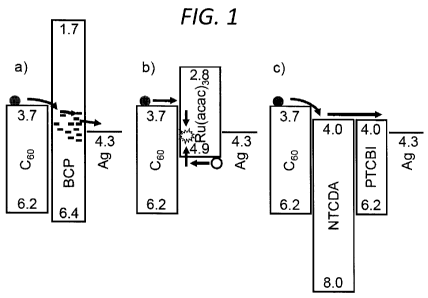
[057] FIG. 1 Shows energy level diagrams of exciton blocking layers that
transport
charge via a) damage-induced trap states, b) electron-hole recombination, and
c) electron
transport through the lowest unoccupied molecular orbital.
- 15 -
CA 02827632 2013-08-16
WO 2012/161773
PCT/US2012/025916
[058] FIG. 2 shows fill factor (FF) under spectrally corrected 1 sun, AM1.5G
illumination for devices with BCP buffer layers (squares), PTCBI (circles),
NTCDA
(triangles), and compound NTCDA/PTCBI (stars) as functions of thickness. Lines
are a guide
to the eye. Inset: the molecular structure of 1-NPSQ.
[059] FIG. 3 shows spectrally corrected short-circuit current (J) under 1 sun,
AM1.5G illumination for devices with BCP buffer layers (squares), PTCBI
(circles), NTCDA
(triangles), and compound NTCDA/PTCBI (stars) as a function of thickness.
Solid lines are a
guide to the eye. The dashed line is Jse modeled based on the optical
intensity in the device
for the case of the NTCDA/PTCBI buffer.
[060] FIG. 4 shows spectrally corrected current density vs. voltage
characteristics in
the 4th quadrant under 1 sun, AM1.5G illumination for optimized devices with
no buffer
(diamond), 5 nm BCP (square), 10 nm PTCBI (circle), 10 nm NTCDA (triangle),
and
compound 15 nm NTCDA/5 nm PTCBI buffers (star).
Detailed Description
[061] Significant progress has been made over the last 25 years in improving
the
efficiency of organic photovoltaic (OPV) cells. An important milestone to
increased
efficiency was the introduction of a buffer layer interposed between the
acceptor layer and
cathode contact, forming a so-called "double heterojunction" solar cell. The
ideal buffer
serves multiple purposes: to protect the underlying acceptor material (e.g.
C60) from damage
due to the evaporation of hot cathode metal atoms, to provide efficient
electron transport to
the cathode, to serve as an exciton blocking layer (EBL) that prevents
excitons generated in
the acceptor from quenching at the cathode, and to act as a spacer that
maximizes the optical
field at the active donor-acceptor heterojunction.
[062] The most commonly used EBLs are wide energy gap (and hence transparent)
semiconductors, such as bathocuproine (BCP), that transport carriers via
cathode metal-
- 16-
CA 02827632 2013-08-16
WO 2012/161773
PCT/US2012/025916
deposition-induced damage that results in a high density of conducting trap
states (Fig. la).
However, as the layer is conductive only in the presence of traps, the
thickness is limited by
the depth of damage (<10 nm), which may not be optimal for achieving a maximum
optical
field intensity in the active region of the device.
[063] One possible route to the use of thicker, wide energy gap EBLs is to
dope the
film to increase its conductivity. A second type of EBL was introduced based
on tris-
(acetylacetonato) ruthenium(III) (Ru(acac)3) and related compounds that have a
small highest
occupied molecular orbital (HOMO) energy. In this case, holes from the cathode
are
transported along the HOMO of Ru(acac)3 and recombine with electrons at the
acceptor/EBL
interface, as shown in Fig. lb.
[064] The inventors have discovered a third type of EBL where the lowest
occupied
molecular orbital (LUMO) is aligned with that of the acceptor, allowing for
low-resistance
transport of electrons directly from acceptor to cathode. It is shown that
3,4,9,10
perylenetetracarboxylic bisbenzimidazole (PTCBI) serves as an efficient
electron conductor
and forms a low energy barrier contact with the Ag cathode. This leads to an
increased fill
factor from FF = 0.60 typical of analogous BCP-based devices, to FF = 0.70.
Additionally,
1,4,5,8-napthalene-tetracarboxylic-dianhydride (NTCDA) is shown to function as
a wide-gap
electron-conducting EBL. By using both NTCDA and PTCBI in a compound blocking
layer
structure as in Fig. lc, an optimal optical spacing is obtained, leading to
increased
photocurrent. This results in a spectrally corrected power conversion
efficiency of lip = 5.1
0.1% under 1 sun, AM1.5G simulated solar illumination, an improvement of >25%
compared
to a conventional device with a BCP blocker.
[065] The HOMO and LUMO energies of C60 are 6.2 and 3.7 eV, respectively,
while BCP has corresponding energies of 6.4 and 1.7 eV, as shown in Fig. 1.
Although the
low LUMO energy of BCP suggests a large barrier to electron extraction at the
cathode,
- 17 -
CA 02827632 2013-08-16
WO 2012/161773
PCT/US2012/025916
transport in BCP occurs through damage-induced trap states created by the
evaporation of hot
metal atoms onto the BCP surface. Because the PTCBI and NTCDA LUMOs
approximately
align with that of C60, electron transport can occur between these materials
in the absence of
damage.
[066] In at least one embodiment, the PV cell is a planar heterojunction cell.
In
another embodiment, is PV cell is a planar-mixed heterojunction cell. In other
embodiments
of the present disclosure, the PV cell is non-planar. For example, the photo-
active region
may form at least one of a mixed heterojunction, planar heterojunction, bulk
heterojunction,
nanocrystalline-bulk heterojunction, and hybrid planar-mixed heterojunction.
[067] Regardless of the type of cell, the organic photosensitive
optoelectronic device
disclosed herein comprises at least one photoactive region in which light is
absorbed to form
an excited state, i.e., "excitons," which may subsequently dissociate in to an
electron and a
hole. Because the dissociation of the exciton will typically occur at the
heterojunction
formed by the juxtaposition of an acceptor layer and a donor layer comprising
the photoactive
region, an exciton barrier layer is typically desired to prevent excitons
generated in the
acceptor from quenching at the cathode.
[068] The device presently disclosed comprises two electrodes comprising an
anode
and a cathode. Electrodes or contacts are usually metals or "metal
substitutes." Herein the
term metal is used to embrace both materials composed of an elementally pure
metal, e.g., Al,
and also metal alloys which are materials composed of two or more elementally
pure metals.
Here, the term "metal substitute" refers to a material that is not a metal
within the normal
definition, but which has the metal-like properties that are desired in
certain appropriate
applications. Commonly used metal substitutes for electrodes and charge
transfer layers
include doped wide bandgap semiconductors, for example, transparent conducting
oxides
such as indium tin oxide (ITO), gallium indium tin oxide (GITO), and zinc
indium tin oxide
- 18-
CA 02827632 2013-08-16
WO 2012/161773
PCT/US2012/025916
(ZITO). In particular, ITO is a highly doped degenerate n+ semiconductor with
an optical
bandgap of approximately 3.2eV rendering it transparent to wavelengths greater
than
approximately 3900 A.
[069] Another suitable metal substitute material is the transparent conductive
polymer polyanaline (PAM) and its chemical relatives. Metal substitutes may be
further
selected from a wide range of non-metallic materials, wherein the term "non-
metallic" is
meant to embrace a wide range of materials provided that the material is free
of metal in its
chemically uncombined form. When a metal is present in its chemically
uncombined form,
either alone or in combination with one or more other metals as an alloy, the
metal may
alternatively be referred to as being present in its metallic form or as being
a "free metal."
Thus, the metal substitute electrodes of the present disclosure may sometimes
be referred to
as "metal-free" wherein the term "metal-free" is expressly meant to embrace a
material free
of metal in its chemically uncombined form. Free metals typically have a form
of metallic
bonding that may be thought of as a type of chemical bonding that results from
a sea of
valence electrons throughout the metal lattice. While metal substitutes may
contain metal
constituents they are "non-metallic" on several bases. They are not pure free-
metals nor are
they alloys of free-metals. When metals are present in their metallic form,
the electronic
conduction band tends to provide, among other metallic properties, a high
electrical
conductivity as well as a high reflectivity for optical radiation.
[070] Herein, the term "cathode" is used in the following manner. In a non-
stacked
PV device or a single unit of a stacked PV device under ambient irradiation
and connected
with a resistive load and with no externally applied voltage, e.g., a solar
cell, electrons move
to the cathode from the adjacent photoconducting material. Similarly, the term
"anode" is
used herein such that in a solar cell under illumination, holes move to the
anode from the
adjacent photoconducting material, which is equivalent to electrons moving in
the opposite
- 19 -
CA 02827632 2013-08-16
WO 2012/161773
PCT/US2012/025916
manner. It will be noted that the terms are used herein anodes and cathodes
may be
electrodes or charge transfer regions.
[071] When a PV cell is operating under illumination, the output photocurrent
is
formed by collecting photo-generated electrons at cathode and photo-generated-
holes at
anode. The dark current flows in the opposite direction due to induced
potential drop and
electric field. Electrons and holes are injected from cathode and anode,
respectively, and can
go to the opposite electrodes if they do not encounter significant energy
barriers. They can
also recombine at the interface to form recombination current. Thermally
generated electrons
and holes inside the active region can also contribute to the dark current.
Although this last
component is dominating when the solar cell is reverse biased, it is
negligible under forward
bias condition.
[072] The dark current of an operating PV cell mainly come from the following
sources: (1) the generation/recombination current /g, due to the electron-hole
recombination
at donor/acceptor interface, (2) the electron leakage current /, due to the
electrons going from
the cathode to the anode through the donor/acceptor interface, and (3) the
hole leakage
current Ih due to the holes going from the anode to the cathode through the
donor/acceptor
interface. In operation a solar cell has no externally applied bias. The
magnitudes of these
current components are dependent on the energy levels. /g, increases with the
decrease of
interfacial gap AEg. le increases with the decrease of AEL, which is the
difference of the
lowest unoccupied molecular orbital (LUMO) energies of the donor and acceptor.
1h increases
with the decrease of AEH, which is the difference of the highest occupied
molecular orbital
(HOMO) energies of the donor and acceptor. Any of these three current
components can be
the dominating dark current depending on the energy levels of the donor and
acceptor
materials.
- 20 -
CA 02827632 2013-08-16
WO 2012/161773
PCT/US2012/025916
[073] In one embodiment, the photo-active region forms at least one of a mixed
heterojunction, bulk heterojunction, nanocrystalline-bulk heterojunction, and
hybrid planar-
mixed heterojunction.
[074] Stacked organic photosensitive optoelectronic devices are further
contemplated herein. The stacked device according to the present disclosure
may comprise a
plurality of photosensitive optoelectronic subcells, wherein at least one
subcell comprises two
electrodes comprising an anode and a cathode in superposed relation; a donor
region between
the two electrodes, the donor region formed of a first photoconductive organic
semiconductor
material; an acceptor region between the two electrodes and adjacent to the
donor region, the
acceptor region formed of a second photoconductive organic semiconductor
material; and at
least one of an electron blocking layer and a hold blocking layer between the
two electrodes,
and adjacent to at least one of the donor region and the acceptor region. Such
stack devices
may be constructed in accord with the present disclosure to achieve high
internal and external
quantum efficiencies.
[075] When the term "subcell" is used hereafter, it refers to an organic
photosensitive optoelectronic construction which may include at least one of
an electron
blocking EBL and a hole blocking EBL in accordance with the present
disclosure. When a
subcell is used individually as a photosensitive optoelectronic device, it
typically includes a
complete set of electrodes, i.e., positive and negative. As disclosed herein,
in some stacked
configurations it is possible for adjacent subcells to utilize common, i.e.,
shared, electrode,
charge transfer region or charge recombination zone. In other cases, adjacent
subcells do not
share common electrodes or charge transfer regions. The term "subcell" is
disclosed herein to
encompass the subunit construction regardless of whether each subunit has its
own distinct
electrodes or shares electrodes or charge transfer regions with adjacent
subunits. Herein the
terms "cell", "subcell", "unit", "subunit", "section", and "subsection" are
used interchangeably
-21-
CA 02827632 2013-08-16
WO 2012/161773
PCT/US2012/025916
to refer a photoconductive region or set of regions and the adjoining
electrodes or charge
transfer regions. As used herein, the terms "stack", "stacked", "multisection"
and "multicell"
refer to any optoelectronic device with multiple regions of a photoconductive
material
separated by one or more electrode or charge transfer regions.
[076] Since the stacked subcells of the solar cell may be fabricated using
vacuum
deposition techniques that allow external electrical connections to be made to
the electrodes
separating the subcells, each of the subcells in the device may be
electrically connected either
in parallel or in series, depending on whether the power and/or voltage
generated by the PV
cell is to be maximized. The improved external quantum efficiency that may be
achieved for
stacked PV cell embodiments of the present disclosure may also be attributed
to the fact that
the subcells of the stacked PV cell may be electrically connected in parallel
since a parallel
electrical configuration permits substantially higher fill factors to be
realized than when the
subcells are connected in series.
[077] In the case when the PV cell is comprised of subcells electrically
connected
in series so as to produce a higher voltage device, the stacked PV cell may be
fabricated so as
to have each subcell producing approximately the same current so to reduce
inefficiency. For
example, if the incident radiation passes through in only one direction, the
stacked subcells
may have an increasing thickness with the outermost subcell, which is most
directly exposed
to the incident radiation, being the thinnest. Alternatively, if the subcells
are superposed on a
reflective surface, the thicknesses of the individual subcells may be adjusted
to account for
the total combined radiation admitted to each subcell from the original and
reflected
directions.
[078] Further, it may be desirable to have a direct current power supply
capable of
producing a number of different voltages. For this application, external
connections to
intervening electrodes could have great utility. Accordingly, in addition to
being capable of
- 22 -
CA 02827632 2013-08-16
WO 2012/161773
PCT/US2012/025916
providing the maximum voltage that is generated across the entire set of
subcells, an
exemplary embodiment the stacked PV cells of the present disclosure may also
be used to
provide multiple voltages from a single power source by tapping a selected
voltage from a
selected subset of subcells.
[079] Representative embodiments of the present disclosure may also comprise
transparent charge transfer regions. As described herein charge transfer
layers are
distinguished from acceptor and donor regions/materials by the fact that
charge transfer
regions are frequently, but not necessarily, inorganic and they are generally
chosen not to be
photoconductiyely active.
[080] The organic photosensitive optoelectronic device disclosed herein may
be
useful in a number of photovoltaic applications. In at least one embodiment,
the device is an
organic photodetector. In at least one embodiment, the device is an organic
solar cell.
Examples
[081] The present disclosure may be understood more readily by reference to
the
following detailed description of exemplary embodiments and the working
examples. It is
understood that other embodiments will become apparent to those skilled in the
art in view of
the description and examples disclosed in this specification.
Example 1
[082] Devices were grown on 150 nm thick layers of indium tin oxide (ITO) pre-
coated onto glass substrates. Prior to deposition, the ITO surface was cleaned
in a surfactant
and a series of solvents and then exposed to ultraviolet-ozone for 10 min
before loading into a
high vacuum chamber (base pressure < 10-7 Ton-) where Mo03 was thermally
evaporated at
0.1 nm/s. Substrates were then transferred to a N2 gloyebox where 2,4-bis[4-(N-
Pheny1-1-
naphthylamino)-2,6-dihydroxyphenyl] squaraine (1-NPSQ, see molecular
structural formula
in Fig. 2, inset) films were spin-coated from heated 6.5 mg/ml solutions in
1,2-
- 23 -
CA 02827632 2013-08-16
WO 2012/161773
PCT/US2012/025916
dichlorobenzene, and thermally annealed on a hot plate at 110 C for 5 min to
promote the
growth of a nanocrystalline morphology.
[083] Substrates were once again transferred into the high vacuum chamber for
deposition of purified organics at 0.1 nm/s, followed by a 100nm thick Ag
cathode deposited
at 0.1 nm/s through a shadow mask with an array of 1 mm diameter openings.
Current density
versus voltage (J- 17)characteristics were measured in an ultra-pure N2
ambient, in the dark
and under simulated AM1.5G solar illumination from a filtered 150 W Xe lamp.
Lamp
intensity was varied using neutral density filters. Optical intensities were
referenced using an
NREL-calibrated Si detector, and photocurrent measurements were corrected for
spectral
mismatch. Errors quoted correspond to the deviation from the average value of
three or more
devices on the same substrate.
[084] Devices were fabricated with the following structure: glass/150 nm
ITO/8
nm Mo03/15 nm 1-NPSQ/40 nm C60/buffer(s)/100 nm Ag. The open-circuit voltage
depended on the interfacial energy gap between the donor and acceptor, and was
found to be
Võ = 0.90 to 0.96 0.01 V, independent of buffer layer composition.
[085] Figure 2 shows FF as a function of buffer layer thickness x for BCP,
PTCBI,
NTCDA, and compound buffers consisting of (x-5) nm NTCDA/5 nm PTCBI. Optimal
performance for devices with BCP occurs at a thickness of 5 nm, with FF = 0.60
0.01,
beyond which there was sharp drop in efficiency due to the limited depth of
damage-induced
transport states extending into the film from the surface. In contrast,
devices with PTCBI
exhibit FF = 0.70 0.01, with only a small reduction as x¨>S0 nm, confirming
the low
resistance transport in this material. The optimum thickness for PTCBI was 10
nm, where lip
decreased for thicker films due to a decrease in short-circuit photocurrent
(J), since PTCBI
absorption overlaped with that of the active acceptor and donor layers.
Devices with NTCDA
buffer layers showed FF = 0.62 0.01. In contrast, devices with a compound 15
nm
- 24 -
CA 02827632 2013-08-16
WO 2012/161773
PCT/US2012/025916
NTCDA/5 nm PTCBI buffer had a FF = 0.68 0.01, which was similar to that of
PTCBI
alone.
[086] The compound NTCDA/PTCBI buffer layer lead to increases in J,õ
compared to PTCBI alone. Unlike PTCBI, the wide energy gap NTCDA was
transparent
across the visible spectrum. Hence, the PTCBI was kept sufficiently thin (5
nm) to provide a
low-barrier cathode contact without introducing excessive optical absorption.
At the same
time, the NTCDA thickness was adjusted to maximize the optical field at the
donor-acceptor
junction without increasing series resistance, contrary to the case with BCP.
The trend in J,õ
as a function buffer layer agreed with optical modeling using the transfer-
matrix approach,
shown by the dashed line in Fig. 3. Optimized devices employing compound
buffers achieve
= 8.0 0.1 mA/cm2 compared to 7.2 0.1 mA/cm2 for BCP and 7.1 0.1 mA/cm2
for
PTCBI, as seen in Fig. 3. For devices without a buffer and with BCP, PTCBI,
NTCDA, and
PTCBUNTCDA buffers, the following values were measured lip = 2.8 0.1, 4.0
0.1, 4.6
0.1, 3.2 0.1, and 5.1 0.1 %, respectively. These results are summarized in
Table 1.
[087] To understand the differences in FF between the several buffer layer
combinations explored, we describe the current density using the ideal diode
equation:
J = J lexp[q(17, ¨ JR,) I nk ¨ 11 ¨ õd(17,)J x , (1)
[088] where 4 is the reverse saturation current, n is the ideality factor, V,
is the
applied voltage, Rs is the series resistance, T is temperature, q is the
electron charge, qppd(17,)
is the field-dependent polaron pair dissociation efficiency, and Jx is the
exciton current
reaching the heterojunction. For optimized BCP, PTCBI, and NTCDA/PTCBI buffer
layer
devices, Rs < 10 n-cm2, indicating efficient transport of electrons to the
cathode. With layers
as thick as 50 nm, Rs for PTCBI and compound buffers does not change
appreciably, while
for BCP it increases to > 10 kn-cm2 for x = 50 nm. Devices with NTCDA-only
buffers have
Rs >100 .Q.-cm2 for all thicknesses, due to an electron extraction barrier
formed at the
- 25 -
CA 02827632 2013-08-16
WO 2012/161773 PCT/US2012/025916
NTCDA/Ag interface, which has been reported to be > 1 eV. However, NTCDA-based
devices that include a 5 nm thick layer of PTCBI have a similar Rs to that of
PTCBI alone, in
good agreement with the previous reports of a < 0.1 eV barrier at the PTCBI/Ag
interface.
One possible mechanism for the difference in FF for devices with BCP or PTCBI
is the effect
of trapped charges on the internal electric field. From Eq. 1, the current
density for a device
under illumination is determined by the field-dependence of Ilppd. Because
electron transport
in BCP occurs through damage-induced traps, their residence in these deep
levels induces an
electric field that is opposite to the field induced by Va, resulting in
increased recombination
at the heterojunction. This appears in the J-V characteristic as an increased
slope at zero bias
(see Fig. 4), leading to a decrease in FF.
[089] The performances of all devices are summarized in Table 1. The values
for
VOC, JSC, fill factor (FF), and power conversion efficiency (ip) were measured
at one sun
standard AM1.5G solar illumination.
Table 1. Performance for devices with different buffer layers under simulated
1
sun (mismatch corrected), AM1.5G illumination.
.Buffer Thickness 1W:n õwr
14yet: (61:Al cat* (%)
:
none 0 0.90 0.59 5.3 2.8 0.1
BCP 5 0.93 0.60 7.2 4.0 0.1
PTCBI 10 0.94 0.70 7.1 4.6 0.1
NTCDA 10 0.94 0.62 5.6 3.2 0.1
NTCDA/PTCBI 15/5 0.95 0.68 8.0 5.1 0.1
[090] As shown, the Inventors have demonstrated the use of electron conducting
EBLs in OPVs. Here, electrons are transported via the LUMO states directly
from that of the
-26-
CA 02827632 2013-08-16
WO 2012/161773
PCT/US2012/025916
acceptor to the cathode. By using PTCBI as a buffer layer, a FF = 0.70 0.01,
compared to
FF = 0.60 0.01 for conventional BCP-based devices. Adding an NTCDA electron-
conducting EBL in combination with PTCBI allows for optimized optical spacing
and
efficient exciton blocking, leading to an increase in lip that is >25 % for an
analogous
squaraine/C60/BCP OPV. The increased stability of PTCBI compared to BCP may
also
potentially extend the operational lifetime of OPVs employing blocking layers.
[091] The specification and examples disclosed herein are intended to be
considered
as exemplary only, with a true scope and spirit of the invention being
indicated in the
following claims.
[092] Other than in the examples, or where otherwise indicated, all numbers
expressing quantities of ingredients, reaction conditions, analytical
measurements, and so
forth used in the specification and claims are to be understood as being
modified in all
instances by the term "about." Accordingly, unless indicated to the contrary,
the numerical
parameters set forth in the specification and attached claims are
approximations that may
vary depending upon the desired properties sought to be obtained by the
present disclosure.
At the very least, and not as an attempt to limit the application of the
doctrine of equivalents
to the scope of the claims, each numerical parameter should be construed in
light of the
number of significant digits and ordinary rounding approaches.
[093] Notwithstanding that the numerical ranges and parameters setting forth
the
broad scope of the disclosure are approximations, unless otherwise indicated
the numerical
values set forth in the specific examples are reported as precisely as
possible. Any numerical
value, however, inherently contains certain errors necessarily resulting from
the standard
deviation found in their respective testing measurements.
-27 -