Note: Descriptions are shown in the official language in which they were submitted.
CA 02827749 2013-08-19
WO 2012/114251 1 PCT/1B2012/050757
DETONATION OF EXPLOSIVES
FIELD OF THE INVENTION
This invention relates to detonation of explosives. More particularly, the
invention
relates to detonator systems for detonating explosives with which they are
arranged
in a detonating relationship. The invention accordingly provides a detonator
system
for detonating an explosive charge with which it is, in use, arranged in a
detonating
relationship. The invention also provides a method of operating a detonator
system.
BACKGROUND TO THE INVENTION
Detonation of explosive charges is generally effected by means of detonators
which
are provided in a detonating relationship with the explosive charges. Such
explosive
charges usually comprise so-called "main" or "secondary" explosives.
In the mining industry, in particular, as well as in a number of other
industries which
rely on the use of explosives, e.g. the demolition industry, accurate control
of
explosives detonation is of great importance, for reasons including safety and
accuracy of blasting operation.
CA 02827749 2013-08-19
WO 2012/114251 2 PCT/1B2012/050757
Generally speaking, one can distinguish between two types of detonators namely
electronic detonators and pyrotechnic detonators.
Electronic detonators, generally, effect detonation of an explosive with which
they are
in a detonating relationship by generating a voltage spark or plasma in
proximity to
the explosive. Such voltage spark or plasma is generated by the breakdown of a
resistive element or bridge which is provided between two conducting
electrodes.
The resistive bridge and the electrodes are generally referred to collectively
as a
"fuse head" which is accommodated within a detonator housing. The plasma
generates a shock wave which is transmitted to the proximate explosive and
initiates
the explosive.
Such electronic detonators generally provide accurate control over detonation,
particularly as regards timing and delay properties thereof. However,
electronic
detonators are expensive to manufacture and difficult to use, requiring a
separate or
external power source and complex electronic transmission wire connections to
allow
transmission of electricity to the detonator and permit remote triggering
thereof. In
the applicant's experience, such connections are, in the Applicant's
experience,
prone to failure and may even result in, or allow for, premature initiation of
the
detonator and thus of the explosive, due to false stimuli, e.g. being provided
by radio-
frequency (rf) interference on the mining/demolition site.
In contrast to electronic detonators operating by means of an electronic delay
system, pyrotechnic detonators employ a series of explosive charges that are
located
within a detonator housing to provide a desired detonating signal to the main
CA 02827749 2013-08-19
WO 2012/114251 3 PCT/1B2012/050757
explosive charge at a required timing and delay. The series of explosive
charges
generally includes (i) an initiating and sealing charge, also known as a
priming
charge, (ii) a timing charge, (iii) a primary charge and, optionally, (iv) a
base charge.
The initiating charge serves to initiate the explosive sequence in response to
a shock
signal transmitted thereto and also functions as a sealing charge which
provides a
seal to prevent blow-back inside the detonator housing. The initiating charge
also
initiates the timing charge which provides a desired burning delay for
detonation.
The timing charge, in turn, initiates the primary charge which either directly
provides
a detonation initiating signal to the main explosive charge, or initiates the
base
charge that, in turn, will provide the desired detonation initiating signal to
the main
explosive charge.
As alluded to above, initiation of the initiating charge of a pyrotechnic
detonator is
generally effected by imparting a shock signal to the detonator, typically
being
provided by one or more shock tubes which are located in an initiating
relationship
with the detonator. The initiating charge then typically comprises a
sensitive
explosive, initiation of which can be effected by a shock wave of sufficient
magnitude.
Shock tube is well known and widely used in the initiation of detonators; it
comprises
a hollow plastic tube lined with a layer of initiating or core explosive,
typically
comprising a mixture of HMX and aluminium metal powder. Upon ignition of the
initiating (core) explosive, a small explosion propagates along the tube in
the form of
an advancing temperature/pressure wave front, typically at a rate of
approximately
7000 ft/s (about 2000m/s). Upon reaching the detonator, the
pressure/temperature
wave triggers or ignites the initiating/sealing charge in the detonator, which
results in
the sequence of ignitions mentioned above and thus eventually causing
detonation of
CA 02827749 2013-08-19
WO 2012/114251 4 PCT/1B2012/050757
the main explosive charge. Although shock tube is economically attractive,
safe and
easy to use, not being readily susceptible to false stimuli, existing
pyrotechnic-based
detonator systems do not at all permit the same extent of control of
detonation timing
and delay which is achieved by using electronic detonators, as the timing and
delay
features are provided by the detonator explosive charge loading, instead of by
electric components.
It will therefore be appreciated that each of electronic and pyrotechnic
detonator
systems has particular disadvantages associated therewith, which disadvantages
impact negatively on the operational reliability, safety and ease of use of
such
systems. More particularly, whilst electronic detonator systems are attractive
from
the perspective of the accuracy of control which they offer, the complex
voltage
transmission wire arrangements and connections which are required present a
concern. As regards pyrotechnic detonator systems, whilst they offer the
ability to
employ shock tube and avoid the use of complex transmission wire, they present
difficulties in achieving detonation delay control and accuracy.
The present invention therefore seeks, broadly, to provide an approach to
operating
explosive detonators which addresses and at least partly alleviates the
disadvantages associated with both pyrotechnic and electronic initiation of
explosive
detonators.
More specifically, the present invention seeks to address the difficulties of
complex
electrical signal transmission wire connections which are associated with the
CA 02827749 2013-08-19
WO 2012/114251 5 PCT/1B2012/050757
operation of electronic detonator systems and also the difficulties of
inaccurate delay
timing and control associated with pyrotechnic detonator systems.
SUMMARY OF THE INVENTION
IN ACCORDANCE WITH ONE ASPECT OF THE INVENTION, there is provided an
explosives detonator system for detonating an explosive charge with which it
is, in
use, arranged in a detonating relationship, the detonator system comprising
a detonator housing;
a detonation circuit inside the detonator housing, the detonation circuit
comprising a conductive pathway;
a fuse head inside the detonator housing, the fuse head comprising at least
two spaced apart conductive electrodes and a resistive bridge spanning a space
between the electrodes, and being integrated with the detonation circuit such
that the
conductive pathway passes along both electrodes and the resistive bridge; and
an uncharged chargeable voltage source inside the detonator housing, the
chargeable voltage source being integrated with the detonation circuit and
being
electrically sensitive to a charging property which is included in a charging
signal that
is, in use, communicated to the detonator, such that exposure to the charging
property charges the voltage source, thereby rendering the voltage source
capable of
generating a potential difference between the electrodes at least to equal the
breakdown voltage of the resistive bridge,
wherein the charging property is any one or more of a charging light pulse, a
charging temperature, a charging pressure and a charging radio frequency of
the
charging signal and the chargeable voltage source is therefore electrically
sensitive
CA 02827749 2013-08-19
WO 2012/114251 6 PCT/1B2012/050757
to any one or more of the charging light pulse, the charging temperature, the
charging pressure and the charging radio frequency.
For continuity with the specification of priority application number
ZA2011/01370 in
particular, it is noted that the detonator system corresponds, broadly, with
the
detonator described in ZA2011/01370. More particularly, the uncharged
chargeable
voltage source comprises, broadly, the integrated voltage source of
ZA2011/01370.
In use, when the generated potential difference between the electrodes equals
or
exceeds the breakdown voltage of the resistive bridge, a voltage spark or
plasma is
generated between the electrodes. This plasma, in turn, generates a shock
signal
which causes, directly or indirectly, initiation and thus detonation of the
explosive
charge with which the detonator system is arranged in a detonating
relationship.
The detonator housing may, in one embodiment of the invention, be of
cylindrical
form.
The detonator may also include a support or substrate on which the detonation
circuit
is provided. In such a case, the support or substrate will thus also be
located inside
the detonator housing. The substrate may typically be a flexible substrate and
may
comprise PET (polyethylene terephtalate), PEN (polyethylene naphthalate), PI
(polyethylene imine) or coated paper.
The conductive pathway of the detonation circuit, and preferably the
detonation
circuit itself, preferably comprises integrated circuitry, thus being
integrated with the
CA 02827749 2013-08-19
WO 2012/114251 7 PCT/1B2012/050757
substrate. In one embodiment of the invention, the conductive pathway may be
etched in to the substrate. Preferably, however, the integrated circuitry is
printed
integrated circuitry, being printed onto the substrate as hereinafter
described in more
detail.
Additionally, at least some, but preferably all, of the components of the
detonation
circuit that are provided along the conductive pathway, i.e. the fuse head
(comprising
both the electrodes and the resistive bridge) and the voltage source, may also
be
printed on the substrate by suitable printing methods as hereinafter described
in
more detail. It is therefore preferred that these components do not comprise
so-
called surface mounted devices (or SMD's).
It will therefore be appreciated that, preferably, the detonation circuit, in
its entirety, is
a printed circuit, not having any SMD's included therein. Printing of the
detonation
circuit, i.e. the conductive pathway and its components, may be by means of
ink jet
printing, gravure, screen printing, off-set lithography, flexography, or any
other
suitable reel to reel method.
The resistive bridge of the fuse head may comprise a resistive element.
Typically,
the resistive element may be a thin-film element, a surface mounted device, or
a
resistive element obtained by chemical-dip a technique. When obtained by a
chemical dip-technique, the resistive element may be applied to the substrate
by
dipping the substrate on which the electrodes are provided in a suitable
chemical, i.e.
oxidizer, fuel and/or explosive, dip and thereafter allowing the chemical to
dry.
Preferably however the resistive element is a printed thin film resistive
element,
CA 02827749 2013-08-19
WO 2012/114251 8 PCT/1B2012/050757
typically being printed with a suitable polymeric or conductive ink, or
metallization
paste which is gold-, copper-, silver-, carbon-, stainless steel- or aluminium-
based.
The paste may also be carbon-based, with the carbon being in the form of
carbon
nanotubes. The energy output from the resistive bridge may be enhanced by
adding
a layer printed in a suitable output enhancement chemical (oxidizer, fuel and
or
explosive). By 'output enhancement', there is referred particularly, but
not
exclusively, to the shock wave that is generated by breakdown of the resistive
bridge.
The electrodes of the fuse head may also be printed on the substrate,
typically also
by using a suitable conductive, e.g. metallic or polymeric, ink or paste as
hereinbefore described.
As will be appreciated, the voltage source is not a pre-charged voltage
source, such
as an electrochemical cell or battery. The detonator system is therefor
provided with
a proviso that the voltage source is not pre-charged and thus not capable, in
the
absence of the charging signal, of generating the breakdown voltage across the
electrodes. The voltage source, and thus the detonator system, can therefore
be
regarded as initially being in a passive state, until it is exposed to the
charging
property of the charging signal.
The detonator system may include shock tube that is provided in initiating
proximity
to the detonator. The charging signal may then be a shock signal which is
provided
by, and propagated along, the shock tube. The shock tube may typically have a
hollow elongate body, inside of which is provided a shock tube explosive,
detonation
of which provides the shock signal. The shock tube may also contain, in
addition to
CA 02827749 2013-08-19
WO 2012/114251 9 PCT/1B2012/050757
the shock tube explosive, a photo-luminescent chemical that provides or
enhances
the charging light pulse. The photo-luminescent chemical may typically be a
fluorescent or phosphorescent chemical or, alternatively, may be a precursor
for a
photo-luminescent chemical, in which case it may be capable of transforming
into a
photo-luminescent chemical under explosive conditions. The photo-luminescent
chemical may, in one embodiment of the invention, be inorganic and comprise a
rare
earth metal salt or combinations of two or more such salts. Typically, the
salts may
be selected from oxide salts, nitrate salts, perchlorate salts, persulphate
salts and
combinations thereof. Alternatively, the photo-luminescent chemical may be a
precursor for such a salt or another luminescent oxide.
Being chargeable in nature, and initially in an uncharged condition, operation
of the
voltage source is dependent on a stimulus provided by an external power or
energy
source. This external energy source is, of course, the charging property of
the
charging signal. It is to be appreciated that such an external power or energy
source
is not regarded as the voltage source, as the generation of the voltage
difference
between the electrodes is achieved by means of the voltage source that is
integrated
with the detonation circuit and not by means of the external power source. The
external power source itself, in the absence of the voltage source, is
therefore not
capable of generating the potential difference across the electrodes.
In one embodiment of the invention, the voltage source may include a
photosensitive
cell, such as a photovoltaic cell. Although the photovoltaic cell may be an
SMD, the
photovoltaic cell preferably is a printed photovoltaic cell that is printed
onto the
substrate. Typically, the photovoltaic cell is an organic photovoltaic (OPV)
cell, such
CA 02827749 2013-08-19
WO 2012/114251 1 PCT/1B2012/050757
0
as a P3HT:PCBM organic photovoltaic cell. The organic photovoltaic cell may be
printed on the substrate, typically with a phenyl-C61-butyric acid methyl
ester
(PCBM)-based ink and a polythiophene-, or more particularly poly(3-
hexylthiophene)
or (P3HT)-based ink.
In another embodiment of the invention, the voltage source may comprise a
passive
electronic component such as a capacitor and a charging component that is
operatively associated with the capacitor along the conductive pathway of the
detonation circuit, thus being capable of charging the capacitor. The charging
component may be electrically sensitive to the charging property, such that
exposure
of the charging component to the charging property results in the charging
component charging the capacitor, thereby rendering the capacitor capable of
generating a potential difference between the electrodes at least equal to the
breakdown voltage of the resistive bridge. The charging component may
therefore
be configured for delivering a charge of sufficient magnitude to the
capacitor, such
that discharge of the capacitor results in the generation of the breakdown
voltage,
unless a voltage booster is employed as hereinafter described. It
is to be
appreciated that, in such an embodiment, the voltage source therefore
comprises
both the capacitor and the charging component. The charging component may
typically comprise one or more transistors that are in electrical
communication with
the voltage source along the conductive pathway of the detonation circuit.
In a further embodiment of the invention, the voltage source may comprise one
or
more transistors, thus in the absence of a passive electrical component such
as a
capacitor and with the transistor itself constituting the voltage source.
CA 02827749 2013-08-19
WO 2012/114251 11 PCT/1B2012/050757
When the charging property comprises the charging light pulse, the transistor,
whether being the charging component or the voltage source, may include a
photosensitive material that is sensitive to the charging light pulse as a
function of its
output voltage, and with a light-activated change in the photosensitive
material at the
charging light pulse resulting in an increase in the transistor output
voltage.
In one embodiment of the invention, the transistor may be operatively
associated, i.e.
form a bulk heterojunction, with an organic photovoltaic cell. For example,
the
transistor may be a pentacene-based organic thin film transistor having a P3HT-
PC61 BM organic photovoltaic cell operatively associated therewith. In such a
case,
photosensitivity is therefore imparted on the transistor by the organic
photovoltaic cell
In another embodiment of the invention, the transistor may comprise a
multilayer
organic thin film transistor, having alternating layers of Cu phthalocyanine
and
3,4,9,10-perylenetetracaboxylic bis-benzimidazole.
In yet a further embodiment of the invention, the transistor may comprise a
bulk
heterojunction, i.e. operative association, of poly(3-octyl thiophene) and
PCBM, being
a derivative of C60.
Still further, the transistor may comprise covalently bonded organic
donor/receptor
dyads.
CA 02827749 2013-08-19
WO 2012/114251 12 PCT/1B2012/050757
When the charging property comprises the charging temperature, the transistor
may
include a temperature sensitive material that is sensitive to the charging
temperature
as a function of its output voltage, with a thermally-activated change in the
temperature sensitive material at the charging temperature thus resulting in
an
increase in the transistor output voltage.
When the charging property comprises the charging pressure, the transistor may
include a pressure sensitive material that is sensitive to the charging
pressure as a
function of its output voltage, with a pressure-activated change in the
pressure
sensitive material at the charging pressure resulting in an increase in the
transistor
output voltage.
As alluded to above, the transistor may, in particular, be an organic thin
film transistor
(OTFT). Alternatively, the transistor may be an organic field effect
transistor (OFET).
The transistor may, in particular, be printed onto the substrate, thus being a
printed
transistor. When the transistor comprises and OTFT or OFET, it may be printed
on
the substrate by means of a suitable organic ink associated with the
components of
the OTFT or OFET.
In yet another embodiment of the invention, the voltage source may comprise an
active of a passive or active radiofrequency identification device (RFID) that
is
sensitive, as a function of its output voltage, to the charging radio
frequency. In such
a case, the charging signal may be a radio signal, having the charging radio
CA 02827749 2013-08-19
WO 2012/114251 13 PCT/1B2012/050757
frequency, which is transmitted to the voltage source, i.e. the RFID, from a
radio
signal transmitter.
In use, the detonator system will initially be in a passive and non-detonable
condition,
with the chargeable voltage source being in the uncharged condition. The
detonator
system is therefore not capable of effecting detonation of an explosive
charge.
However, once the charging signal is transmitted to the voltage source,
whether by
means of a shock signal propagated along the shock tube or by means of a radio
signal transmitted by a radio transmitter, the voltage source becomes charged
and
thus capable of generating the breakdown voltage across the electrodes.
Generation
of an electric detonation signal is thereby achieved through transmission of
an
analogue, or rather pyrotechnic-based, initiating signal (comprising the
charging
signal).
The detonator system may also include, as part of the detonation circuitry, an
electronic delay device that delays generation of the breakdown voltage over
the
electrodes for a desired delay period. Electronic delay is therefore
maintained, whilst
the requirement for complex electric transmission wire connections is obviated
by
enabling the use of shock tube.
The detonator system may typically further include one or more trigger
components
that are sensitive to one or more of the charging properties, typically as a
function of
their conductance or conductivity. Such trigger components may be also be
integrated with the detonation circuitry and may initially obstruct the
generation of the
breakdown voltage, until they are exposed to the charging property to which
they are
CA 02827749 2013-08-19
WO 2012/114251 14 PCT/1B2012/050757
sensitive and which results in their conductance increasing. With their
conductance
increased, the obstruction which they provided is therefore removed and
generation
of the breakdown voltage is allowed. Such trigger components may typically
include
one or more transistors that include materials that are sensitive, as a
function of their
conductance, to one or more of the charging properties of the charging signal.
It is
envisaged that, in this manner, at least one charging property can be used to
charge
the voltage source and at least one other charging property can be used to
trigger
the detonator system for generation of the breakdown voltage.
IN ACCORDANCE WITH ANOTHER ASPECT OF THE INVENTION, there is
provided, in an explosives detonator system comprising a detonator that has a
detonator housing inside which is provided a detonator circuit that comprises
a
conductive pathway, having integrated therewith (i) a fuse head, comprising at
least
two spaced apart conductive electrodes and a resistive bridge spanning a space
between the electrodes, and (ii) an uncharged chargeable voltage source that
is
electrically sensitive to a charging property comprising at least one of a
charging light
pulse, a charging pressure, a charging temperature and a charging radio
frequency,
such that exposure to the charging property charges the voltage source,
thereby
rendering the voltage source capable of generating a potential difference
between
the electrodes at least to equal the breakdown voltage of the resistive
bridge, a
method of operating the detonator system includes
electrically charging the chargeable voltage source by transmitting a charging
signal, having the charging property, to the voltage source; and
generating, by means of the voltage source, a potential difference greater
than
the breakdown voltage of the resistive bridge between two electrodes.
CA 02827749 2013-08-19
WO 2012/114251 15 PCT/1B2012/050757
The detonator system may, in particular, be a detonator system as hereinbefore
described and thus in accordance with the invention.
The charging signal may be provided by shock tube that is arranged in
initiating
proximity to the detonator. In particular, the charging signal may comprise a
shock
signal of the shock tube. When the charging property is a charging radio
frequency,
the charging signal may be a radio signal having the charging radio frequency.
BRIEF DESCRIPTION OF THE DRAWINGS
The invention will now be described by way of illustrative example only with
reference
to the accompanying diagrammatic drawing, which shows, conceptually, a
detonator
system in accordance with the invention.
DETAILED DESCRIPTION OF THE INVENTION
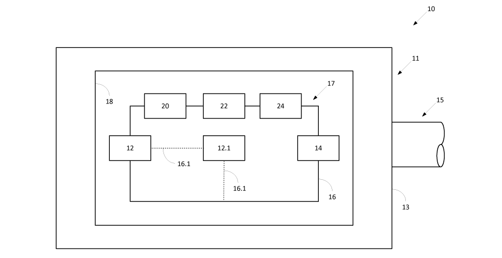
Referring to the drawing, reference numeral 10 generally indicates an
explosive
detonator system in accordance with the invention.
The detonator system 10 comprises an electronic time delay detonator 11 and
shock
tube 15 which is connected to the detonator 11, more particularly to a
cylindrical
housing 13 of the detonator 11. The shock tube 15 is thus in initiating
proximity to
the detonator 11. It is to be appreciated that the shock tube 15 needs not be
physically connected to the detonator 11 in all embodiments.
CA 02827749 2013-08-19
WO 2012/114251 16 PCT/1B2012/050757
The detonator 11 includes a voltage source 12 and a fuse head 14 which are
operatively connected along a conductive pathway 16. The conductive pathway
16,
along with the voltage source 12 and the fuse head 14, provides a detonation
circuit
that is generally indicated by reference numeral 17.
It will be appreciated that the detonator 11 does not include any pyrotechnic
compositions and that the detonator system 10 therefore comprises a
combination of
a pyrotechnic detonator system, being represented by the shock tube 15, and an
electronic detonator system, being represented by the electronic detonator 11.
The detonator 11 includes a support or substrate 18 on which the detonator
circuit is
provided. The substrate 18 is thus located inside the detonator housing 13.
The
substrate is a flexible substrate, being of any one of PET, PEN, PI or coated
paper.
The conductive pathway 16 comprises integrated circuitry, either being etched
into
the substrate 18 or, more preferably, being printed onto the substrate by
means of
ink jet, gravure, screen printing, off-set lithography, flexography and other
reel to reel
methods.
Similarly, at least some, but preferably all, of the components of the
detonation circuit
17 provided along the conductive pathway 16, i.e. the voltage source 12 and
the fuse
head 14 (comprising both the electrodes and the resistive bridge), are also
printed on
the substrate 18. Thus, it is preferred that these components do not comprise
so-
called surface mounted devices (SMD's).
CA 02827749 2013-08-19
WO 2012/114251 17 PCT/1B2012/050757
The fuse head 14 comprises two spaced apart conductive electrodes (not
illustrated)
with a resistive bridge (not illustrated) spanning a space between the
electrodes.
The conductive pathway 16 passes along both electrodes and the resistive
bridge.
The resistive bridge comprises a resistive element. , being either a thin-film
element
or a surface mounted device. Typically, the resistive element may be a thin-
film
element, a surface mounted device, or a resistive element obtained by chemical-
dip
a technique. When obtained by a chemical dip-technique, the resistive element
may
be applied to the substrate by dipping the substrate on which the electrodes
are
provided in a suitable chemical, i.e. oxidizer, fuel and/or explosive, dip and
thereafter
allowing the chemical to dry. Preferably however the resistive element is a
printed
thin film resistive element, being printed on the substrate 18 with a suitable
polymeric
or conductive ink, or metallization paste which is gold-, copper-, silver-,
carbon-,
stainless steel- or aluminium-based. The paste can also be carbon-based, with
the
carbon being in the form of carbon nanotubes. The energy output from the
resistive
bridge can be enhanced by adding an enhancement layer thereto, printed in a
suitable chemical (oxidizer, fuel and or explosive).
The electrodes of the fuse head are also preferably printed on the substrate
18 with a
suitable conductive, e.g. metallic or polymeric, ink or paste as hereinbefore
described.
The shock tube 15 has a hollow elongate body, inside of which is provided a
shock
tube explosive, detonation of which provides a shock signal.
CA 02827749 2013-08-19
WO 2012/114251 18 PCT/1B2012/050757
The voltage source 12 is an uncharged chargeable voltage source which is
electrically sensitive to a charging property which is included in a charging
signal that
is, in use, communicated to the detonator system 10. In particular, exposure
to the
charging property charges the voltage source 12, thereby rendering the voltage
source 12 capable of generating a potential difference between the electrodes
of the
fuse head 14, which potential difference is at least equal to the breakdown
voltage of
the resistive bridge.
Generation of such a potential difference between the
electrodes results in the generation of a voltage spark or plasma between the
electrodes due to breakdown of the resistive bridge. This voltage spark or
plasma is
used then to initiate or detonate an explosive with which the detonator 10 is
arranged
in a detonating relationship.
In accordance with the invention, the charging property comprises any one or
more
of a charging light pulse, a charging pressure, a charging temperature and a
charging
radio frequency. The voltage source 12 is thus electrically sensitive to any
one or
more of the charging light pulse, the charging pressure, the charging
temperature
and the charging radio frequency
In one embodiment of the invention, the voltage source 12 comprises a
photosensitive cell, such as a photovoltaic cell. Although the photovoltaic
cell may
be an SMD, the photovoltaic cell preferably is a printed photovoltaic cell
that is
printed onto the substrate. In
particular, the photovoltaic cell is an organic
photovoltaic cell such as a P3HT:PCBM organic photovoltaic cell. The organic
photovoltaic cell is also preferably printed on the substrate, typically with
a phenyl-
CA 02827749 2013-08-19
WO 2012/114251 19 PCT/1B2012/050757
C61-butyric acid methyl ester (PCBM)-based ink and a polythiophene, or more
particularly poly(3-hexylthiophene) or (P3HT)-based ink.
Alternatively, the voltage source 12 comprises a capacitor and a charging
component
12.1 comprising a transistor that is operatively connected to the capacitor
along the
conductive pathway 16. The charging component 12.1, i.e. the transistor, is
therefore configured for delivering a charge of sufficient magnitude to the
capacitor,
such that discharge of the capacitor results in the generation of the
breakdown
voltage, unless a voltage booster is employed as hereinafter described.
In the drawing, the charging component 12.1 is included in the conductive
pathway
16 along alternative route 16.1. The charging component 12.1 is electrically
sensitive
to the charging property, such that exposure of the charging component 12.1 to
the
charging property results in the charging component 12.1 charging the
capacitor,
thereby rendering the capacitor capable of generating a potential difference
between
the electrodes. Sensitivity of the transistor, as the charging component 12.1,
to the
charging property is achieved in the manner hereinafter described.
In yet a further embodiment of the invention, the voltage source 12 may
comprise
one or more transistors, selected from organic thin film transistors and
organic field
effect transistors. The transistor is, in such an embodiment, therefore
configured for
delivering a charge of sufficient magnitude to the capacitor, such that
discharge of
the capacitor results in the generation of the breakdown voltage, unless a
voltage
booster is employed as hereinafter described.
CA 02827749 2013-08-19
WO 2012/114251 20 PCT/1B2012/050757
Regardless of whether the transistor is the voltage source 12 or the charging
component 12.1, when the charging property comprises the charging light pulse,
the
transistor, in one embodiment includes, for providing sensitivity to the
charging light
pulse, a photosensitive material that is sensitive to the charging light pulse
as a
function of its output voltage such that a light-activated change in the
photosensitive
material at the charging light pulse results in an increase in the transistor
output
voltage. More particularly, the transistor, in one embodiment, includes an
organic
photovoltaic cell that provides a photoconductive material constituting the
photosensitive material. In such an embodiment, the transistor is
operatively
associated, i.e. forms a bulk heterojunction, with the organic photovoltaic
cell. For
example, the transistor can be a pentacene-based organic thin film transistor
having
a P3HT-PC61BM organic photovoltaic cell operatively associated, i.e. forming a
bulk
heterojunction, therewith. In another embodiment of the invention, the
transistor
comprises, for rendering it sensitive to the charging light pulse, a
multilayer organic
thin film transistor, having alternating layers of Cu phthalocyanine and
3,4,9,10-
perylenetetracaboxylic bis-benzimidazole. In yet a further embodiment of the
invention, for rendering it sensitive to the charging light pulse, the
transistor
comprises a bulk heterojunction, i.e. operative association, of poly(3-octyl
thiophene)
and PCBM, being a derivative of C60. Still further, the transistor can
possibly
comprise, for rendering it sensitive to the charging light pulse, covalently
bonded
organic donor/receptor dyads.
When the charging property comprises the charging temperature, the transistor
includes, for providing sensitivity to the charging temperature, a temperature
sensitive material that is sensitive to the charging temperature as a function
of its
CA 02827749 2013-08-19
WO 2012/114251 21 PCT/1B2012/050757
output voltage such that a thermally-activated change in the temperature
sensitive
material at the charging temperature results in an increase in the transistor
output
voltage. The temperature sensitive material is typically a polymeric
ferroelectric
material, preferably a polyvinylidene fluoride (PDVF). In such a case the
temperature
sensitive material is present in the transistor as a piezo- or pyroelectric
polymer thin
film capacitor that has thus been integrated with the transistor.
When the charging property comprises the charging pressure, the transistor
includes,
for providing sensitivity to the charging pressure, a pressure sensitive
material that is
sensitive to the charging pressure as a function of its output voltage and
with a
pressure-activated change in the pressure sensitive material at the charging
pressure
resulting in an increase in the transistor output voltage. The pressure
sensitive
material may include a pressure sensitive rubber, constituting a layer of the
transistor, and/or a pressured sensitive laminate, constituting an external
laminate of
the transistor.
More particularly, the transistor may thus typically comprise an integration
of an
organic thin film transistor (OTFT) with the pressure sensitive material. The
pressure
sensitive material may, in particular, have a variable resistance that is a
function of its
mechanical deformation, thus imparting a change in conductivity to the OTFT at
the
switching pressure that is sufficient for the conductivity to be conducive to
the
generation of the detonation initiating voltage. One example of such a
material is
pressure sensitive rubber that contains carbon particles and a silicon rubber
matrix.
Another example of a device utilising pressure sensitive rubber for pressure
detection
is one based of space-charge limited transistors (SCLT), having P3HT as an
active
CA 02827749 2013-08-19
WO 2012/114251 22 PCT/1B2012/050757
layer. A SCLT is a vertical transistor with a grid electrode inserted between
source
electrode and drain electrode to control the vertical current flow. As
pressure is
applied to the pressure sensitive rubber the resistance and therefore current
in the
source-drain circuit is systematically changed allowing the applied pressure
to be
monitored. Another possibility is the employment of a flexible pressure
sensor,
possibly through employment of transparent plastic foil as both the substrate
and
gate dielectric of the transistor 18.1. When the pressure sensitive material
comprises
a laminate, the laminate may typically be a polydimethylsiloxane (PDMS) mold
with
gold electrodes. It is to be noted, however, that OTFT's have an inherent
sensitivity
to applied pressure, for example pentacene transistors having a solution-
processed
polyvinylphenol gate dielectric on a glass substrate.
In accordance with the invention, the voltage source can also be an active or
a
passive radiofrequency identification device (RFID) that is sensitive, as a
function of
its output voltage, to the charging radiofrequency. In such a case, the
charging
signal comprises a radio signal, having the charging radio frequency.
When the charging property is one or more of the charging light pulse, the
charging
temperature and the charging pressure, the charging signal will be the shock
signal
that is provided by and propagated along the shock tube 15. For the purpose of
providing the charging light pulse, the shock tube 15 can also contain a photo-
luminescent chemical that provides or amplifies the charging light pulse. The
photo-
luminescent chemical is preferably a fluorescent and/or phosphorescent
chemical or
a chemical precursor to a fluorescent and/or phosphorescent chemical.
CA 02827749 2013-08-19
WO 2012/114251 23 PCT/1B2012/050757
When the charging property is the charging radio frequency, the charging
signal will
be a radio signal that is provided by a radio transmitter and has the charging
radio
frequency.
The detonator 11 also optionally includes, as part of the detonation circuit
17, an
electronic delay device 20 that delays generation of the breakdown voltage
across
the electrodes for a desired delay period. Electronic delay is therefore
maintained,
whilst the requirement for complex electric transmission wire connections is
obviated
by use of a non-electronic charging signal.
The detonator 11 further optionally includes, as part of the detonation
circuit 17, one
or more trigger components 22 that are sensitive to one or more of the
charging
properties, typically as a function of their conductance or conductivity. Such
trigger
components 22 are integrated with the detonation circuit 17 and initially
obstruct the
generation of the breakdown voltage, until they are exposed to the charging
property
to which they are sensitive and which results in their conductance increasing.
With
their conductance increased, the obstruction which the trigger components 22
provided is therefore removed and generation of the breakdown voltage is
allowed.
Such trigger components typically include one or more transistors that include
materials that are sensitive, as a function of their conductance, to one or
more of the
charging properties of the charging signal. Such transistors may be
transistors as
hereinbefore described, thus including such electrically sensitive materials
as also
hereinbefore described. With such a configuration, at least one charging
property
can be used to charge the voltage source and at least one other charging
property
can be used to trigger the detonator system for generation of the breakdown
voltage.
CA 02827749 2013-08-19
WO 2012/114251 24 PCT/1B2012/050757
In use, detonator system 10 is arranged such that the detonator 11 is in
detonating
proximity to and thus in a detonating relationship with an explosive that is
to be
detonated thereby. Initially, the voltage source 12 is uncharged and thus not
capable
of generating the breakdown voltage across the electrodes of the fuse head 14.
The
detonator 11 is this not capable, in this condition, of detonating the
explosive. This
situation subsists, and the detonator 11 thus remains in a dormant condition,
until the
voltage source 12 is exposed to the charging property of the charging signal.
In detonating the explosive, the charging signal is transmitted to the
detonator 11,
whether by transmission of the radio signal from the radio transmitter or by
initiating
the shock tube 15. Once the charging property of the charging signal
encounters the
voltage source 12, with the voltage source 12 thus having been exposed to the
charging property, the voltage source 12 becomes charged and thus rendered
capable of generating the breakdown potential difference between the
electrodes of
the fuse head 14 and thus of detonating the explosive.
If no delay device 20 or detonation trigger 22 is provided, the charged
voltage source
will, on becoming fully charged for generation of the breakdown voltage,
immediately
discharge, thus causing breakdown of the resistive bridge and generation of
the
voltage plasma, with the explosive thereby being detonated. When the detonator
11,
however, includes the delay device 20, discharge of the device will be delayed
according to the specification of the device 20. Similarly, when the detonator
11
includes the detonation trigger 22, the charged voltage source 12 will
discharge only
CA 02827749 2013-08-19
WO 2012/114251 25 PCT/1B2012/050757
when the trigger 22 allows the discharge, e.g. on receipt of a charging signal
charging property that only reaches the detonator 11 after another charging
property.
It is to be appreciated that it is envisaged that a voltage booster 24 may be
required
in order to boost the voltage that is provided by the voltage source 12 for
the purpose
of generating the breakdown voltage. Such a voltage booster may, in itself, be
a
transistor.
The applicant expects that a detonator system such as the detonator system 10
according to the present invention, i.e. a detonator incorporating therein a
voltage
source as opposed to a detonator which is reliant on an external voltage
source, will
be particularly useful in obviating the requirement for complex conducting
wire
connections which is usually associated with electronic detonators (as
hereinbefore
described).
The applicant believes in particular that the combination of a non-electronic
or
analogue detonation signal (being the charging signal) with an electronic
detonation
effect, combines the advantages of both the pyrotechnic-based detonator
(safety of
use provided by shock tube) and the electronic detonator (accuracy of timing
and
delay), as hereinbefore described, whilst obviating the difficulties
associated with
both.
The applicant expects that the invention will improve the safety of usage of
explosive
detonators in that the risk of failure will be reduced and greater accuracy of
detonation and timing will be attained. The applicant therefore expects that a
CA 02827749 2013-08-19
WO 2012/114251 26 PCT/1B2012/050757
detonator in accordance with the invention will allow for greater accuracy and
reliability of detonators used in detonating explosives and addresses the
difficulties
and concerns that are associated with purely pyrotechnic and purely electric
detonators respectively.