Note: Descriptions are shown in the official language in which they were submitted.
CA 02827919 2013-08-21
TITLE OF THE INVENTION
Electrode foil, current collector, electrode, and electric energy storage
element
using same
TECHNICAL FIELD
[0001]
The present invention relates to a solid electrolytic capacitor having a solid
electrolyte layer (typically, an electrically conductive polymer layer) formed
thereinside,
and an electrode foil usable in such a type of capacitor. The present
invention further
relates to a current collector, an electrode, and an electric energy storage
element such
as a secondary battery, an electric double layer capacitor or a hybrid
capacitor, using the
electrode.
BACKGROUND ART
[0002]
(Background Art regarding Solid Electrolytic Capacitor)
Late years, operating frequencies of electronic devices have become higher and
higher. Along with this trend, an electrolytic capacitor as one electronic
component
also needs to be provided as a product having excellent impedance properties
in a higher
operating frequency range than before. In order to cope with the need, various
solid
electrolytic capacitors using, as a solid electrolyte, an electrically
conductive polymer
with a high electrical conductivity, have been developed. This type of
solid
electrolytic capacitor is excellent, particularly, in high-frequency
properties, in addition
to life and temperature properties, and thereby widely employed in electric
circuits for
personal computers, and others.
[0003]
In one simplest example, a wound-type solid electrolytic capacitor can be
produced by a process comprising a step (i) of: subjecting a surface of an
anode
aluminum foil to a chemical conversion treatment to form an oxide film
thereon;
laminating the resulting anode aluminum foil to a cathode aluminum foil
through a
1
CA 02827919 2013-08-21
separator sheet; connecting a lead member to each of the two foils; and
winding the
laminate to prepare a capacitor element, and a step (ii) of: placing the
prepared capacitor
element in an aluminum casing; immersing the capacitor element in an
electrically
conductive polymer solution to cause thermal polymerization of an electrically
conductive polymer under heating to form a solid electrically conductive
polymer layer
between the two foils. When the anode aluminum foil is used as an anode, and
the
cathode aluminum foil and the electrically conductive polymer layer
electrically
connected to the cathode aluminum foil are used as a cathode, the anode and
the cathode
are connected through the electrically insulating oxide film, so that it
becomes possible
to achieve charge and discharge between the anode and cathode.
[0004]
In the above solid electrolytic capacitor, the cathode aluminum foil is not
subjected to a chemical conversion treatment, so that no artificially formed
oxide film
exists thereon. However, actually, an oxide film is also formed on the cathode
aluminum foil, due to natural oxidation during production or use. In this
case, the
solid electrolytic capacitor is generally formed in a layered structure
comprising (i) the
anode aluminum foil, (ii) the oxide film on the anode aluminum foil, (iii) the
electrically
conductive layer, (iv) the natural oxide film on the cathode aluminum foil,
and (v) the
cathode aluminum foil. This is equivalent to a state in which two capacitors
are
connected in series to each other, which causes a problem that a capacitance
of the solid
electrolytic capacitor as a whole is reduced.
[0005]
In order to cope with this problem, researches have been conducted to prevent
a
capacitance component from being generated in a cathode to thereby allow an
increase
in capacitance of a capacitor. In this connection, some cathode foils obtained
from the
conventional researches and a problem involved in the conventional cathode
foils will
be described below.
[0006]
JP 2007-036282 A and JP 2007-019542 A disclose a cathode foil obtained by
forming a chemical conversion coating film on a surface of a cathode aluminum
foil,
2
CA 02827919 2013-08-21
and further forming a metal nitride such as TiN, or a metal carbide such as
TiC, on the
chemical conversion coating film by vapor deposition. However, a metal such as
Ti,
and a nitride or carbide thereof, are insufficient in resistance to thermal
oxidation.
Thus, in the cathode foil, a problem occurs that an oxide film will grow
through a heat
treatment included in a capacitor production process, resulting in generation
of a
capacitance component, and increase in ESR (Equivalent Series Resistance).
[0007]
JP 2006-190878 A discloses a cathode foil obtained by forming a carbon film
on a surface of a metal having a valve function. However, when a carbon film
is
directly formed on a metal foil such as an aluminum foil, a problem occurs
that an ESR
is increased due to poor adhesion between the metal foil and the carbon film.
[0008]
JP 2006-100478 A discloses a cathode foil obtained by forming a
carbon-containing layer on a surface of an aluminum foil, wherein an
intervening layer
consisting of fibrous or filamentous aluminum carbide (A14C3, aluminum carbide
whisker) is formed between the surface of the aluminum foil and the carbon-
containing
layer to provide enhanced adhesion therebetween. However, in this cathode
foil, the
carbon-containing layer is a layer consisting of carbon in the form of
particles, so that
the surface of the aluminum foil and the carbon-containing layer come into
point
contact with each other. Thus, there is a problem that an interfacial
resistance is
increased due to the small contact area. Further, the carbon-containing layer
is formed
by a process of applying a carbon-containing substance on the surface of the
aluminum
foil and fixedly attaching carbon particles thereonto through a thermally
drying
treatment, which causes difficulty in forming the carbon-containing layer to
have a
sufficiently small thickness, and also gives rise to a problem that a electron
transfer
distance between the Al layer and a solid electrolyte layer becomes longer,
thereby
causing an increase in ESR. Moreover, this cathode foil is insufficient in
water
resisting property (water resistance), and, particularly in high-temperature
environments,
a problem occurs that the aluminum carbide whisker as an electron transfer
pathway is
cut, causing deterioration in electrical conductivity.
3
[0009]
JP 2009-049376 A discloses a cathode foil obtained by forming, by a vacuum
vapor deposition method, a Ni layer on a roughened surface of an aluminum
foil. The
description of JP 2009-049376 A says that a Ni oxide film formed on a surface
of the Ni
layer is a semiconductor, i.e., has electrical conductivity, which makes it
possible to
realize a lower ESR in a capacitor. However, deterioration in electrical
conductivity
due to formation of the oxide film cannot be negligible, and a semiconductor
is
inadequate as a film component substance. It is desirable that at least a top
layer of the
film is formed using an electrically conductive substance excellent in
oxidation resisting
property (oxidation resistance).
[0010]
As another type of cathode foil for use in an electrolytic capacitor
configured to
operate using a driving electrolytic solution, instead of a solid electrolyte,
JP
2007-095865 A discloses a cathode foil obtained by vapor-depositing a metal
such as Ti
on a roughened surface of an aluminum foil to form a metal film thereon, and
further
applying thereon a binder having carbon fine particles dispersed thereover,
wherein the
applied binder is subjected to a heating treatment to fix the carbon fine
particles on the
metal film. However, in the cathode foil described in JP 2007-095865 A, a
surface of
the Ti film is oxidized by the driving electrolytic solution, so that a large
resistance is
generated in an interface between a layer composed of the Ti film and a layer
consisting
of carbon, causing an increase in ESR of a capacitor (it is mentioned that, in
order to
suppress an influence of the oxidation of Ti, the cathode foil described in JP
2007-095865 A is preferably subjected to a surface roughening treatment such
as
etching). Moreover, supposing that it is used as a solid electrolytic
capacitor, an oxide
film will grow through a heat treatment included in a capacitor production
process,
causing an increase in ESR. Further, when the Ti film is joined to carbon by a
binder
or the like, a large interfacial resistance is also generated in a joined
portion, causing an
increase in ESR of a capacitor.
[0011]
4
CA 2827919 2018-05-11
CA 02827919 2013-08-21
It is generally described that, in a solid electrolytic capacitor, when a
surface of
a cathode foil is appropriately roughened, a contact area with a solid
electrolyte
becomes larger, and thereby the ESR is reduced. However, the effect is small.
Moreover, when a surface of an aluminum substrate is roughened, for example,
by an
etching treatment, a space occurs between the aluminum substrate and a film
formed
inside pores resulting from the surface-roughening, so that the surface
becomes unstable
due to a reaction occurring in the space by a chemical agent and water used in
a
capacitor production process, and an interface between the aluminum substrate
and the
film is more likely to be oxidized by oxygen diffusion, thereby causing
problems such
as an increase in interfacial resistance, and acceleration in degradation of a
capacitor.
Further, there is another problem that the surface roughening treatment leads
to an
increase in capacitor production cost.
[0012]
As above, in the conventional cathode foil where a metal film is formed on an
aluminum foil, there is a problem that a surface of the film is oxidized, so
that, when an
oxidation reaction is progressed due to temporal change or the like, a cathode
will have
a capacitance. Further, in the conventional cathode foil where a carbon layer
is formed
on an aluminum foil directly or through a metal film or the like, if adhesion
between
layers is insufficient, a surface of the aluminum foil or a surface of the
metal layer in
contact with carbon is oxidized, so that a cathode will have a capacitance.
Therefore, a
capacitance of a solid electrolytic capacitor as a whole is reduced, as
previously
mentioned. Moreover, each of the above conventional cathode foils has problems
such
as an increase in ESR and an increase in cost.
[0013]
(Background Art regarding Secondary Battery, Electric Double Layer Capacitor,
Hybrid Capacitor, etc.)
Late years, in view of multi-functionalization of mobile electronic devices,
improvement in fuel economy of automobiles and transport and construction
vehicles,
spread of distributed renewable energy, upgrading and expanding of back-up
power
supply in case of disaster/emergency, etc., demand for an electric energy
storage
element to be mounted thereto has become larger over the years. In the
electric energy
storage element including an electric double layer capacitor, a hybrid
capacitor and a
secondary battery, there is a need for further enhancing a power density
(W/kg, W/L)
and life property.
[0014]
In view of performance such as handling/processing strength and electrical
conductivity, productivity, production cost, etc., a current collector
composed of a metal
foil is used in an electrode constituting the electric energy storage element,
in many
cases. The electrode is constructed by forming, on a current collector, an
electrode
layer which comprises an active substance, an electrically conductive
assistance and a
binder. When adhesion, electrical conductivity and/or chemical stability
between the
current collector and the electrode layer is insufficient, a satisfactory
power density
cannot be obtained due to an increase in contact resistance, thereby causing
difficulty in
rapid charging/discharging. Further, for example, along with a charge-
discharge cycle
of the electric energy storage element, an interface between the current
collector and the
electrode layer is likely to be transformed over time due to a chemical change
such as
oxidation, or the electrode layer is likely to be peeled from the current
collector, thereby
causing an increase in internal resistance and a reduction in usable life.
[0015]
In this connection, for example, JP 11-250900 A describes a battery obtained
by
forming a carbon film layer between a current collector and an active
substance layer.
[0016]
However, when the carbon film layer is directly formed on the metal foil,
adhesion, electrical conductivity and chemical stability between the metal
foil and the
carbon film layer are insufficient, so that a contact resistance between the
current
collector and the electrode layer will be gradually increased, which leads to
problems,
such as a reduction in power density and an increase in internal resistance,
thereby
causing difficulty in rapid charging/discharging. In addition, according to
inventers'
search, there are JP 2011-142100 A, JP 2010-218971 A, JP 2009-283275 A, and JP
6
CA 2827919 2019-02-21
CA 02827919 2013-08-21
2008-270092 A as related prior art document. However, film configurations
disclosed
therein have the same problems.
SUMMARY OF THE INVENTION
[0018]
The present invention has been made to solve the above conventional technical
problems. Specifically, in a cathode foil for a solid electrolytic capacitor,
which is
obtained by forming a film on an aluminum foil, it is an object of the present
invention
to prevent generation of a capacitance in a cathode by enhancing resistance to
oxidation
of each layer constituting the film, and adhesion between respective layers.
In this
type of cathode foil, it is another object of the present invention to prevent
generation of
a large interfacial resistance due to a rapid change in composition within the
film,
thereby allowing a reduction in ESR and LC (Leakage Current) of a capacitor.
[0019]
Further, with a view to solving the problems in the conventional techniques as
disclosed in JP 11-250900 A, JP 2011-142100 A, JP 2010-218971 A, JP 2009-
283275 A,
and JP 2008-270092 A to minimize an increase in internal resistance over a
long period
of time and maintain a high power density, thereby allowing rapid
charging/discharging
and realizing an electric energy storage element excellent in life property,
it is yet
another object of the present invention to enhance adhesion and electrical
conductivity
between a current collector and an electrode layer, and suppress
transformation of an
interface between the current collector and the electrode layer due to a
chemical change.
[0020]
In order to solve the above problems, the present invention provides an
electrode material which is characterized in that it is constructed by
forming, on an
electrode substrate, a first electrically conductive layer, a mixed layer
containing carbon
and a substance composing the first electrically conductive layer in a mixed
state, and a
second electrically conductive layer consisting substantially of carbon,
wherein the
7
CA 02827919 2013-08-21
mixed layer is configured to have a composition which changes from a state
containing
substantially only the substance composing the first electrically conductive
layer to a
state containing substantially only carbon, in a direction from the first
electrically
conductive layer to the second electrically conductive layer.
[0021]
In the electrode material provided by the present invention, the mixed layer
containing respective components of the first and the second electrically
conductive
layers in a mixed state is formed between the two electrically conductive
layers, so that
it becomes possible to enhance adhesion between the substance composing the
first
electrically conductive layer and the carbon. This feature solves the
conventional
technical problem that, due to an insufficient adhesion between the carbon and
the
substance composing the first electrically conductive layer, the substance
composing the
first electrically conductive layer is oxidized, thereby causing the electrode
material to
have a capacitance, and further causing an increase in ESR. In addition, the
second
electrically conductive layer consists substantially of carbon, so that it is
excellent in
oxidation resistance. Further, in a
boundary region with the first electrically
conductive layer, the mixed layer contains substantially only the substance
composing
the first electrically conductive layer, whereas, in a boundary region with
the second
electrically conductive layer, the mixed layer contains substantially only the
carbon.
This precludes the problem that a composition of the electrode material
rapidly changes
in the boundary region, thereby causing generation of a large interfacial
resistance.
[0022]
In the above description, the term "containing substantially only the
substance
composing the first electrically conductive layer" does not necessarily mean
that any
component other than the substance composing the first electrically conductive
layer is
not contained at all. For example, depending on: limitations in production
techniques
concerning control of each component purity in each layer, and mixing of
impurities;
and a level of capacitance as an allowable error of the electrode material in
each product,
an actual composition in the boundary region between the mixed layer and each
of the
8
electrically conductive layers can variously change. The same applies to the
terms
"consisting substantially of carbon" and "containing substantially only
carbon".
[0023]
Further, in the above description, the term "the mixed layer is configured to
have a composition which changes from a state containing substantially only
the
substance composing the first electrically conductive layer to a state
containing
substantially only carbon, in a direction from the first electrically
conductive layer to the
second electrically conductive layer" does not necessarily mean that a content
rate of
carbon in the mixed layer monotonically increases in the direction from the
first
electrically conductive layer to the second electrically conductive layer. For
example,
depending on a variation in each component concentration caused by limitations
in
production techniques, an actual composition at each position within the mixed
layer
can variously change. However, it is preferable that the mixed layer is formed
to allow
the carbon content rate to continuously increase in the direction from the
first
electrically conductive layer to the second electrically conductive layer.
[0024]
The first electrically conductive layer may contain at least one selected from
the group consisting of Ta, Ti, Cr, Al, Nb, V, W, Hf, Cu, nitrides of the
metals and
carbides of the metals. A substance usable in the first electrically
conductive layer
constituting the electrode material of the present invention is not limited to
the above
substances. However, in the case where an aluminum substrate is used as the
electrode
substrate, in view of energy efficiency and adhesion with the aluminum
substrate, it is
preferable to use the above cited substances, and particularly to use a metal
such as Ti
and Al (as long as adhesion with the substrate or electrical conductivity in
the first
electrically conductive layer is not impaired, a plurality of elements such as
an alloy
may be contained). It should be understood that a material usable as the
electrode
substrate is not limited to aluminum, but may be any suitable material, such
as: Ta, Ti or
Nb as a valve-functional metal; or an aluminum alloy prepared by adding any of
such
materials to aluminum.
[0025]
9
CA 2827919 2019-02-21
CA 02827919 2013-08-21
In the electrode material of the present invention, it is not an essential
requirement to roughen a surface of the electrode substrate. As described in
aftermentioned Examples based on performance test data, even if an electrode
substrate
is not subjected to surface roughening during preparation of the electrode
material of the
present invention, a solid electrolytic capacitor using the electrode
substrate has
excellent capacitance, ESR and leakage current properties, than before. In
particular,
the aftermentioned Examples show that the electrode substrate of the present
invention
prepared without subjecting an electrode substrate to surface roughening has
excellent
heat resisting property (heat resistance), as compared to an electrode
material with a
surface-roughened electrode substrate.
[0026]
The present invention also provides a solid electrolytic capacitor which
comprises an anode foil, a cathode foil, a separator provided between the
anode and
cathode foils, and a solid electrolyte layer formed between the anode and
cathode foils.
The solid electrolytic capacitor is characterized in that the aforementioned
electrode
material is used as the cathode foil.
[0027]
The electrode material of the present invention is particularly suitable for
use as
a cathode foil in a wound-type or stacked-type solid electrolytic capacitor.
Other than
that, it is usable in various capacitors including an electrolytic capacitor
configured to
operate using an electrolytic solution, an electric double layer capacitor, a
lithium ion
capacitor, a lithium ion battery, a solar battery and others.
[0028]
Specifically, the electrode material of the present invention may be modified
by
additionally forming a layer consisting of activated carbon, on the second
electrically
conductive layer consisting substantially of carbon. The resulting electrode
material
can be used as a positive or negative electrode for an electric double layer
capacitor (the
modified electrode material having this configuration can be used as a
positive electrode
of a lithium ion capacitor without any change). Further, the electrode
material of the
present invention may be modified by additionally forming a layer consisting
of a
CA 02827919 2013-08-21
Li-containing active substance, on the second electrically conductive layer.
The
resulting electrode material can be used as a positive electrode of a lithium
ion battery.
That is, the electrode material of the present invention may be used as an
electrode as it is, or may be used as an anode or cathode (positive or
negative electrode)
of any storage device in an additionally-modified state, if necessary, such as
in a state
wherein an additional layer is formed as described above.
[0029]
The solid electrolyte layer may contain at least one selected from the group
consisting of manganese dioxide (Mn02), tetracyanoquinoditnethane (TCNQ),
polyethylenedioxythiophene (PEDOT), polyani line (PAN 1) and polypyrro le.
However,
any suitable electrolyte other than them may also be used. As one example,
formation
of a solid electrolyte layer consisting of PEDOT may be performed by heating a
capacitor element while immersing it in a mixed solution of 3,4-
ethylenedioxythiophene
and p-toluenesulfonic acid iron(II) salt, to thermally polymerize an
electrolyte.
[0030]
As one typical embodiment of the electrode material, the present invention
provides a cathode foil for use in a solid electrolytic capacitor having a
capacitor
element which comprises an anode foil, a cathode foil, a separator provided
between the
anode and cathode foils, and a solid electrically conductive polymer layer
formed
between the anode and cathode foils. The cathode foil is characterized in that
it
comprises: an aluminum foil having a non-roughened surface; a metal layer
formed on
the aluminum foil and consisting substantially of Ti or Al; a mixed layer
formed on the
metal layer and containing carbon and Ti or Al in a mixed state; and a carbon
layer
formed on the mixed layer and consisting substantially of carbon, wherein the
mixed
layer is configured to have a composition which changes from a state
containing
substantially only Ti or Al to a state containing substantially only the
carbon, in a
direction from the metal layer to the carbon layer.
[0031]
This cathode foil corresponds to one typical embodiment of the present
invention which will be described in the aftermentioned Examples based on
11
CA 02827919 2013-08-21
performance test data. However, it is apparent that an embodiment for solving
the
aforementioned conventional technical problems is not limited thereto.
[0032]
For example, as is evident from aftermentioned performance tests, even when
an aluminum substrate in the cathode foil of the present invention has a
roughened
surface, a solid electrolytic capacitor using it has excellent properties than
before, in
terms of capacitance, etc., and a material usable as the electrode substrate
is not limited
to aluminum, as previously mentioned. With regard to a material for use in the
metal
layer, it is also preferable to use Ti or Al, in view of adhesion with
aluminum.
However, any other material having excellent adhesion with aluminum, such as
Ta or Cr.
may also be used. Further, when an electrode substrate made of a different
material is
used, the metal layer may be formed using a material suitable for the
substrate. For
example, when a cupper foil is used as the electrode material, a metal layer
consisting of
Cr having excellent adhesion with the cupper foil may be formed, for example,
by ion
plating. In this case, it is assumed that Cr penetrates through a natural
oxide film on a
surface of the copper foil and binds directly to the copper foil, and that
this provides
high electrical conductivity while suppressing generation of a capacitance
component,
whereby it becomes possible to obtain the same properties as those in the case
where the
metal layer consisting of Ti or Al is formed on an aluminum foil.
[0033]
In the cathode foil of the present invention, the mixed layer containing
respective components of the metal layer and the carbon layer in a mixed state
is formed
between the two layers. It is apparent that enhancement in metal-carbon
adhesion
based on introduction of the above mixed layer can be obtained in the same
manner as
that in the case where the metal layer is formed using a material other than
Ti or Al, and
it is assumed that the enhanced adhesion makes it possible to prevent
formation of an
oxide film on the metal and suppress generation of a capacitance in the
cathode foil.
Further, in a boundary region with the metal layer, the mixed layer contains
substantially only Ti or Al, whereas, in a boundary region with the carbon
layer, the
mixed layer contains substantially only the carbon. Thus, it is apparent that
the effect
12
CA 02827919 2013-08-21
of preventing rapid composition changes in the boundary regions to suppress an
interfacial resistance at a low level can be obtained in the same manner as
that in the
case where the metal layer is formed using a material other than Ti or Al.
[0034]
Further, in order to solve the problems in the conventional techniques as
disclosed in JP 11-250900 A, JP 2011-142100 A, JP 2010-218971 A, JP 2009-
283275 A,
and JP 2008-270092 A, the present invention provides a current collector for
an
electrode, which is characterized in that it is constructed by forming, on a
substrate
containing a metal, a first electrically conductive layer containing a metal,
a mixed layer
containing carbon and a substance composing the first electrically conductive
layer
containing a metal in a mixed state, and a second electrically conductive
layer
consisting substantially of carbon, wherein the mixed layer is configured to
have a
composition which changes from a state containing substantially only the
substance
composing the first electrically conductive layer containing a metal to a
state containing
substantially only carbon, in a direction from the first electrically
conductive layer
containing a metal to the second electrically conductive layer.
[0035]
In the current collector provided by the present invention, the first
electrically
conductive layer containing a metal and the mixed layer containing respective
components of the first electrically conductive layer containing a metal and
the second
electrically conductive layer consisting substantially of carbon, in a mixed
state, are
formed between the surface of the substrate containing a metal and the second
electrically conductive layer, so that it becomes possible to enhance adhesion
between
the substrate and the first electrically conductive layer, and adhesion
between the first
electrically conductive layer and the second electrically conductive layer,
thereby
enhancing electrical conductivity and chemical stability in each interface.
This feature
solves the conventional technical problem that, due to insufficiency of
adhesion
between the substrate and the carbon and insufficiency of electrical
conductivity in an
interface and chemical stability in an interface, a contact resistance between
the current
collector and the electrode layer is increased, and, along with repeated use,
an internal
13
CA 02827919 2013-08-21
resistance of the current collector is increased, causing a reduction in power
density of
the electrode. In addition,
the second electrically conductive layer consists
substantially of carbon, so that it is excellent in electrical conductivity
and in resistance
against a chemical change such as oxidation. Further, in a boundary region
with each
of the first and second electrically conductive layers, a region of the mixed
layer on the
side of the first electrically conductive layer contains only the substance
composing the
first electrically conductive layer, whereas, a region of the mixed layer on
the side of the
second electrically conductive layer contains substantially only the carbon.
This
precludes the problem that a rapid composition change occurs in the boundary
region,
thereby causing generation of a large interfacial resistance.
[0036]
In the above description, the term "containing substantially only the
substance
composing the first electrically conductive layer containing a metal" does not
necessarily mean that any component other than the substance composing the
first
electrically conductive layer containing a metal is not contained at all. For
example,
depending on: limitations in production techniques concerning control of each
component purity in each layer, and mixing of impurities; and a level of
adhesion or
contact resistance as an allowable error of the current collector in each
product, an
actual composition in the boundary region between the mixed layer and each of
the
electrically conductive layers can variously change. The same applies to the
terms
"consisting substantially of carbon" and "containing substantially only
carbon".
[0037]
Further, in the above description, the term "the mixed layer is configured to
have a composition which changes from a state containing substantially only
the
substance composing the first electrically conductive layer containing a metal
to a state
containing substantially only carbon, in a direction from the first
electrically conductive
layer containing a metal to the second electrically conductive layer" does not
necessarily
mean that a content rate of carbon in the mixed layer monotonically increases
in the
direction from the first electrically conductive layer to the second
electrically
conductive layer. For example,
depending on a variation in each component
14
concentration caused by limitations in production techniques, an actual
composition at
each position within the mixed layer can variously change. However, it is
preferable
that the mixed layer is formed to allow the carbon content rate to
continuously increase
in the direction from the first electrically conductive layer to the second
electrically
conductive layer.
[0038]
The first electrically conductive layer may contain at least one selected from
the group consisting of Ta, Ti, Cr, Al, Nb, V, W, Hf, Cu, nitrides of the
metals and
carbides of the metals. A substance usable in the first electrically
conductive layer
constituting the current collector of the present invention is not limited to
the above
substances. However, in the case where an aluminum foil is used as the
substrate
containing a metal, in view of energy efficiency and adhesion with the
aluminum foil, it
is preferable to use the above cited substances, and particularly to use a
metal such as Ti
and Al (as long as adhesion with the substrate or electrical conductivity in
the first
electrically conductive layer is not impaired, a plurality of elements such as
an alloy
may be contained).
[0039]
Carbon for use in the second electrically conductive layer is not particularly
limited. However, in view of increasing a power density of an electric energy
storage
element, it is preferable to use graphite-like carbon which is particularly
excellent in
electrical conductivity among carbon materials. It is also preferable to use
it in view of
production cost. As used here, the term "graphite-like carbon" means carbon
having
an amorphous structure in which two types of bonds: diamond bond (carbon-
carbon
bond based on sp3 hybridized orbital); and graphite bond (carbon-carbon bond
based on
sp2 hybridized orbital), exist in a mixed state, wherein a rate of the
graphite bond is over
one-half. However, in addition to the amorphous structure, a phase having a
crystal
structure partially composed of a graphite structure (i.e., hexagonal crystal
structure
composed of sp2 hybridized orbital-based bonds).
[0040]
CA 2827919 2019-02-21
CA 02827919 2013-08-21
A material usable as the substrate containing a metal is not limited to
aluminum,
but may be a metal foil made of any suitable material, such as: Ti, Cu, Ni,
Hf, or
stainless steel, or an aluminum alloy prepared by adding any of such materials
to
aluminum. A metal foil as a current collector for use in a positive electrode
and a
negative electrode of each electric energy storage element is selected in view
of
electrochemical stability, electrical conductivity, weight, processability,
production cost
and others, while considering an electrolyte and an operating potential of an
active
substance. When the electric energy storage element is an electric double
layer
capacitor, it is preferable to use an aluminum foil for both positive and
negative
electrodes. When it is a hybrid capacitor or a secondary battery, it is
preferable to use
an aluminum foil for a positive electrode and use an aluminum or copper foil
for a
negative electrode.
[0041]
In the current collector of the present invention, it is not an essential
requirement to roughen a surface of the substrate containing a metal. However,
as
described in the aftermentioned Examples based on performance test data, when
the
substrate is subjected to surface roughening during preparation of the current
collector
of the present invention, adhesion between the current collector and the
electrode layer
and collection capability are enhanced, which is more advantageous to
enhancement in
power density and life property. This comes largely from enhancement in
adhesion
strength based on a physical anchor effect between the current collector and
the
electrode layer, and a contact resistance reduction effect based on an
increase in contact
area therebetween, in addition to the aforementioned effects of the first
electrically
conductive layer containing a metal, the mixed layer and the second
electrically
conductive layer. Particularly, in a hybrid capacitor and a secondary battery
where an
active substance repeats volume expansion and contraction caused by occlusion
(intercalation) and release (deintercalation) of ions, surface-roughening of
the substrate
is more effective. Means for surface-roughening is not limited. However, when
an
aluminum or copper foil is used as a material for the substrate, as mentioned
above, it is
preferable to perform the surface-roughening, for example, by chemical or
16
CA 02827919 2013-08-21
electrochemical etching using an acid or alkaline solution, which is a method
capable of
facilitating achieving a porous structure effective for enhancing adhesion
based on an
anchor effect with the electrode layer, and excellent in productivity. In a
hybrid
capacitor such as a lithium ion capacitor, and a secondary battery such as a
lithium ion
secondary battery, when it is necessary to perform a pre-dope operation of
allowing
alkali metal ions or alkaline-earth metal ions to be evenly occluded in an
active
substance of a positive electrode and/or a negative electrode in the electric
energy
storage element, a through-hole may be provided in the metal foil, depending
on a type
of production technique, and production convenience.
[0042]
A total thickness of layers including the mixed layer from the first
electrically
conductive layer to the second electrically conductive layer is not
particularly limited.
For example, this thickness may be set to 45 nm or less. In this case, it
becomes
possible to prevent an electron transfer distance between the current
collector and the
electrode layer from becoming longer, thereby further enhancing the internal
resistance
reducing effect. Particularly, when the metal foil is subjected to surface-
roughening,
the current collector may be prepared to allow the total thickness to become
smaller.
This makes it possible to prevent a film formed on the current collector from
filling a
fine and delicate porous structure formed in the metal foil by etching or the
like, and
impairing the anchor effect and the contact area increasing effect, and evenly
form the
first and second electrically conductive layer on an inner wall having the
porous
structure. In the case where the current collector is used in a negative
electrode of a
hybrid capacitor or a secondary battery, carbon itself composing the second
electrically
conductive layer can serve as an active substance capable of occluding and
releasing
alkali metal ions or alkaline-earth metal ions. In this case, in order to
obtain sufficient
energy density (Wh/kg, Wh/L) as an electric energy storage element, an active
substance-containing electrode layer is required to have a layer thickness of
at least 1
um or more. However, in view of productively, production cost, etc., it is
undesirable
to form the second electrically conductive layer to have a thickness of about
1 pm, for
the purpose of using it as an active substance. Preferably, an
active
17
CA 02827919 2013-08-21
substance-containing electrode layer is formed as a separate layer from the
second
electrically conductive layer constituting the current collector of the
present invention.
[0043]
The present invention provides a secondary battery, such as a lithium ion
secondary battery, a sodium ion secondary battery, a magnesium ion secondary
battery
or a calcium ion secondary battery, which comprises: a positive electrode
formed with
an electrode layer comprising an active substance including a transition metal
oxide or
transition metal phosphate compound containing an alkali metal or an alkali
earth metal,
an electrically conductive assistant, and a binder; and a negative electrode
formed with
an electrode layer comprising an active substance including at least one
selected from
the group consisting of a carbon material capable of occluding and releasing
an alkali
metal ion or alkali earth metal ion, Sn, Si or silicon oxide, S or sulfide,
and titanium
oxide, an electrically conductive assistant, and a binder. The secondary
battery is
characterized in that it comprises an electrode using the above current
collector, wherein
the electrode is used as the positive electrode and the negative electrode. In
this case,
for example, the transition metal oxide or transition metal phosphate compound
containing an alkali metal or an alkali earth metal, which is included in the
active
substance of the positive electrode used in the above secondary battery,
includes
LiCo02, LiMn204, LiNi02, Li(Ni-Mn-Co)02, Li(Ni-Co-A1)02, LiFePO4, NaCr02,
NaFe02, MgHf(Mo04)3, Ca3Co206 and Ca3CoMn06.
[0044]
The present invention provides an electric double layer capacitor using: a
positive electrode formed with an electrode layer comprising an active
substance
including activated carbon or carbon nanotube, an electrically conductive
assistant, and
a binder; and a negative electrode formed with the same layered structure. The
electric
double layer capacitor is characterized in that it comprises an electrode
using the above
current collector, wherein the electrode is used as the positive electrode and
the negative
electrode.
[0045]
18
CA 02827919 2013-08-21
Further, the present invention provides a hybrid capacitor, such as a lithium
ion
capacitor, which comprises a positive electrode formed with an electrode layer
comprising an active substance including activated carbon or carbon nanotube,
an
electrically conductive assistant, and a binder; and a negative electrode
formed with an
electrode layer comprising an active substance including at least one selected
from the
group consisting of a carbon material capable of occluding and releasing an
alkali metal
ion or alkali earth metal ion, Sn, Si or silicon oxide, S or sulfide, and
titanium oxide, an
electrically conductive assistant, and a binder. The hybrid capacitor is
characterized in
that it comprises an electrode using the above current collector, wherein the
electrode is
used as the positive electrode and the negative electrode.
[0046]
In the electrode material of the present invention, interlayer adhesion is
enhanced by forming the mixed layer between the first and second electrically
conductive layers formed on the electrode substrate, so that it becomes
possible to
prevent oxidation of the substance composing the first electrically conductive
layer. In
addition, in a boundary region between the mixed layer and each of the first
and second
electrically conductive layers, the mixed layer consists substantially only of
a
component of a respective one of the first and second electrically conductive
layers,
which precludes an increase in interfacial resistance due to a rapid change in
composition of the electrode material in the boundary region. The use or this
electrode
material as a cathode foil allows a solid electrolytic capacitor to achieve an
increase in
capacitance and a reduction in ESR and leakage current.
[0047]
In addition, as shown by the aftermentioned performance test data, the
electrode material of the present invention is extremely excellent in heat
resistance, so
that it is almost free of quality deterioration even after used under high
temperature for a
long period of time. Further, even when a thickness of a film composed of the
first
electrically conductive layer, the mixed layer and the second electrically
conductive
layer and formed on an aluminum substrate is reduced to about 0.02 m, almost
no
19
CA 02827919 2013-08-21
deterioration in properties of a cathode foil in the electrode material of the
present
invention is observed, and, during preparation of the cathode foil, there is
no need for
roughening a surface of the electrode substrate, so that it becomes possible
to reduce a
material to be used, and simplify a production process, thereby significantly
reducing a
production cost. When the film is formed to have such a reduced thickness, it
becomes
to reduce a risk that crack occurs during winding of the cathode foil.
Furthermore,
when the film is formed to have such a reduced thickness, an electron transfer
distance
between the electrode substrate and the solid electrolyte is reduced, so that
it becomes
possible to further reduce the ESR.
[0048]
In the current collector of the present invention, interlayer adhesion and
electrical conductivity, and chemical stability, are enhanced by forming the
mixed layer
between the first and second electrically conductive layers formed on the
electrode
substrate, so that it becomes possible to prevent transformation due to a
chemical
change such as oxidation, in each of the surface of the substrate and the
substance
composing the first electrically conductive layer. In addition, in a boundary
region
between the mixed layer and each of the first and second electrically
conductive layers,
the mixed layer consists substantially only of a component of a respective one
of the
first and second electrically conductive layers, which precludes an increase
in interfacial
resistance due to a rapid change in composition of the electrode material in
the
boundary region. A positive or negative electrode obtained by forming, on the
above
current collector, an electrode layer comprising an active substance, an
electrically
conductive assistant and a binder is excellent in electrical conductivity,
collection
capability from the electrode layer to the current collector, and chemical
stability, and is
capable of maintaining high adhesion between the current collector and the
electrode
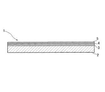
layer over a long period of time. In an electric energy storage element such
as a
secondary battery, an electric double layer capacitor or a hybrid capacitor,
using the
above electrodes, it becomes possible to enhance a power density, while
minimizing a
voltage drop during charging/discharging and suppressing a temperature rise of
the
element during charging/discharging with a large current. Thus, rapid
charging/discharging can be continuously performed for a long period of time
to
achieve a significant extension of a charge-discharge cycle life.
BRIEF DESCRIPTION OF THE DRAWINGS
100491
FIG. 1 is a sectional view illustrating a layered structure of a cathode foil
according to one embodiment of the present invention.
FIG. 2 is an exploded diagram illustrating a structure of a wound-type solid
electrolytic capacitor according to one embodiment of the present invention.
FIG. 3 is a graph for comparing capacitances measured in respective samples of
a solid electrolytic capacitor using a cathode fo.1 according to one
embodiment of the
present invention and a solid electrolytic capacitor using a conventional
cathode foil.
FIG. 4 is a graph for comparing ESRs measured in respective samples of a solid
electrolytic capacitor using a cathode foil according to one embodiment of the
present
invention and a solid electrolytic capacitor using a conventional cathode
foil.
FIG. 5 is a graph for comparing leakage currents measured in respective
samples of a solid electrolytic capacitor using a cathode foil according to
one
embodiment of the present invention and a solid electrolytic capacitor using a
conventional cathode foil.
FIG. 6 is a graph for comparing change rates of capacitances before and after
test measured by subjecting, to a heat resistance test, respective samples of
a solid
electrolytic capacitor using a cathode foil according to one embodiment of the
present
invention and a solid electrolytic capacitor using a conventional cathode
foil.
FIG. 7 is a graph for comparing change rates or ESRs before and after test
measured by subjecting, to a heat resistance test, respective samples of a
solid
electrolytic capacitor using a cathode foil according to one embodiment of the
present
invention and a solid electrolytic capacitor using a conventional cathode
foil.
FIG. 8 is a sectional view illustrating a layered structure of a current
collector
according to one embodiment of the present invention.
21
CA 2827919 2018-05-11
CA 02827919 2013-08-21
FIG. 9 is a sectional view illustrating a layered structure of a positive or
negative electrode according to one embodiment of the present invention.
FIG. 10a is an exploded diagram illustrating a structure of a lithium ion
secondary battery according to one embodiment of the present invention.
FIG. 10b is a diagram illustrating an external structure of a lithium ion
secondary battery according to one embodiment of the present invention.
FIG. 11 illustrates a comparison result of discharge rate properties measured
in
respective samples of a lithium ion secondary battery using a current
collector according
to one embodiment of the present invention and a lithium ion secondary battery
using a
current collector as a comparative sample.
FIG. 12 illustrates a comparison result of charge-discharge cycle lives
measured
in respective samples of a lithium ion secondary battery using a current
collector
according to one embodiment of the present invention and a lithium ion
secondary
battery using a current collector as a comparative sample.
FIG. 13 illustrates a SAICAS test result which compares current
collector-electrode layer adhesion strengths measured in respective samples of
a
positive electrode for a lithium ion secondary battery using a current
collector according
to one embodiment of the present invention and a positive electrode for a
lithium ion
secondary battery using a current collector as a comparative sample.
DESCRIPTION OF EMBODIMENTS
[0050]
As one embodiment of the present invention, a cathode foil in which a first
electrically conductive layer consisting of Ti or Al, a mixed layer containing
carbon and
Ti or Al in a mixed state, and a second electrically conductive layer
consisting of carbon,
are formed on an aluminum foil having a non-roughened surface, and a solid
electrolytic
capacitor prepared using the cathode foil, will now be described. However, as
previously mentioned, each of the aluminum foil used as a substrate and the Ti
or Al for
forming the first electrically conductive layer can be substituted by other
material, and
22
CA 02827919 2013-08-21
the cathode foil of the present invention has excellent properties even when a
surface of
the substrate is roughened, as described later using performance test data.
[0051]
Cathode Foil of the Present Invention
FIG. 1 is a sectional view illustrating a layered structure of a cathode foil
1
according to this embodiment. The cathode foil 1 comprises: a plain aluminum
foil 2
which is not subjected to surface-roughening by an etching treatment or the
like; a metal
layer 3 formed on the plain aluminum foil 2 and composed of a metal film
consisting of
Ti or Al; a mixed layer 4 formed on the metal layer 3 and containing carbon
and the Ti
or Al in a mixed state; and a carbon layer 5 formed on the mixed layer 4.
[0052]
As the plain aluminum foil 2, it is possible to use a commercially available
high-purity aluminum sheet. A thickness of the aluminum sheet is not
particularly
limited. However, when used as a cathode foil for a wound-type solid
electrolytic
capacitor, the aluminum sheet preferably has a thickness of 20 p.m to 50
[0053]
The metal layer 3 is formed by: placing the plain aluminum foil 2 and a metal
material of Ti or Al as a vaporization source, within a vacuum chamber;
vaporizing and
ionizing Ti or Al, for example, by using electron beam and plasma generation
electrodes; and introducing generated positive metal ions to the plain
aluminum foil 2.
In this process, a negative bias voltage is applied to the plain aluminum foil
2, so that
the metal ions directed toward the plain aluminum foil 2 are accelerated to
have high
energy (ion plating method). Thus, Ti or Al ions penetrates through a natural
oxide
film formed on the surface of the plain aluminum foil 2 and strongly adheres
to the plain
aluminum foil 2. In cases where a layer consisting of nitride or carbide of a
metal such
as Ti or Al is formed on the plain aluminum foil 2, the first electrically
conductive layer
may be formed by performing the above process, for example, in a nitrogen gas
or
methane gas atmosphere.
[0054]
23
CA 02827919 2013-08-21
Other than the ion plating method, as a method for forming the metal layer 3,
it
is possible to use a vacuum vapor deposition method, a chemical vapor
deposition
(CVD) method or a sputtering method. However, in view of an advantage of being
able to allow the metal layer 3 and the plain aluminum foil 2 to strongly
adhere to each
other through the natural oxide film, thereby suppressing an ESR of a
capacitor at a
lower level, and an advantage of being able to facilitate formation of a
smooth metal
film, it is preferable to use the ion plating method.
[0055]
The mixed layer 4 can be formed, for example, by an ion plating method, as
with the metal layer 3. That is, in addition to the metal material of Ti or
Al, a carbon
material may be provided as a vaporization source to perform a film formation
process
simultaneously using the two vaporization sources. The introduction of the
mixed
layer 4 makes it possible to enhance adhesion between the metal and the carbon
to
thereby prevent formation of an oxide film.
[0056]
Preferably, the mixed layer 4 is configured such that, in a boundary region
with
the metal layer 3, it contains substantially only Ti or Al, whereas, in a
boundary region
with the carbon layer 5, it contains substantially only carbon, wherein it is
particularly
configured such that a content rate of carbon continuously increases in a
direction from
the metal layer 3 to the carbon layer 5. As one example, the mixed layer 4 can
be
formed by: (i) during an initial stage of film formation for the mixed layer
4, irradiating
only a metal material with an electron beam to form a film consisting only of
Ti or Al;
(ii) along with an elapse of time, gradually reducing an irradiation amount of
electron
beam for the metal material, while increasing an irradiation amount of
electron beam for
a carbon material, to form a mixed film containing the metal and carbon in a
mixed state,
wherein a content rate of carbon gradually increases in a direction toward a
top of the
deposit; and (iii) during a final stage of the film formation, setting the
irradiation
amount of electron beam for the metal material to zero to form a film
consisting only of
carbon. On the other hand, when the mixed layer 4 is formed by a sputtering
method,
the mixed layer 4 having the preferred configuration can be formed by any
suitable
24
CA 02827919 2013-08-21
process, for example, by, along with an elapse of time, gradually reducing a
voltage
applied to a metal target (gradually reducing a sputtering rate of the metal
target), while
gradually increasing a voltage applied to a C target (gradually increasing a
sputtering
rate of the C target).
[0057]
Incidentally, among the aftermentioned performance test data, data of
inventive
samples 7 to 12 is measured using a cathode foil 1 obtained by forming a mixed
layer 4
using the above ion plating method, particularly, in such a manner as to allow
a content
rate of carbon to continuously increase in a direction from the metal layer 3
to the
carbon layer 5. However, it is assumed that, even if the mixed layer 4
partially has a
region where the carbon content rate gradually decreases in the direction
toward the
carbon layer 5 (this situation can occur due to limits of film forming
techniques), it is
possible to obtain excellent properties as compared to a conventional cathode
foil.
This is because, even in such a region, the presence of carbon and Ti or Al in
a mixed
state provides enhanced adhesion between the two component layers, and
therefore
prevents oxidation of the Ti or Al layer to suppress generation of an internal
capacitance
in a cathode. Further, in the cases where the carbon content rate
discontinuously
changes in a partial region of the mixed layers 4, it is considered that the
ESR property
is deteriorated to some extent due to an increase in interfacial resistance in
the partial
region. However, it is assumed that the same properties as a cathode foil can
be
obtained because the adhesion between the two component layers is enhanced by
the
presence of carbon and Ti or Al in a mixed state (with regard to this point,
see data of
inventive samples 1 to 6 among the aftermentioned performance test data).
[0058]
The carbon layer 5 can be formed, for example, by an ion plating method, as
with the metal layer 3 and the mixed layer 4. Typically, the carbon layer 5
can be
formed by, after reducing the irradiation amount of electron beam for the
metal material
to zero in the process of forming the mixed layer 4, continuing the film
formation for a
given time by successively irradiating only the carbon material with an
electron beam.
[0059]
CA 02827919 2013-08-21
Preferably, the carbon layer 5 of the present invention is formed using an ion
plating method or the like, instead of a method of dispersing carbon fine
particles in a
binder, and then applying and heating the obtained mixture, as in a cathode
foil
described in JP 2007-095865 A. This is because a carbon fine particle layer
formed
using a binder comes into point contact with a lower Ti or Al layer, causing
an increase
in interfacial resistance and deterioration in adhesion therebetween. It is
desirable to
form the carbon layer 5 as a smooth and dense carbon film.
[0060]
It is sufficient if each of the metal layer 3, the mixed layer 4 and the
carbon
layer 5 has a thickness of about 0.005 to 0.01 gm. Further, as shown in the
aftermentioned performance test, at least when a total thickness of the three
layers is
0.02 11111 or more, good properties as a cathode foil can be obtained.
However, the
thickness of each of the layers may further be increased.
[0061]
Preferably, each of the metal layer 3, the mixed layer 4 and the carbon layer
5
is formed by the same film forming method. This is because a production
process can
be simplified so as to significantly reduce a production cost. However, each
of the
layers may be formed by a different method.
[0062]
Solid Electrolytic Capacitor of the Present Invention
FIG 2 is an exploded diagram of a wound-type solid electrolytic capacitor 6
prepared using the cathode foil 1. The solid electrolytic capacitor 6 is
prepared by the
following method: (i) after laminating an anode foil 7 obtained by forming an
oxide film
on an anode aluminum foil through a chemical conversion treatment, to a
cathode foil 8
having the layered structure illustrated in FIG 1, through a separator sheet
9, connecting
an anode terminal 11 and a cathode terminal 12, respectively, to the anode
foil 7 and the
cathode foil 8, and winding the laminate to prepare a capacitor element 10;
and
(ii) after inserting the capacitor element 10 in an aluminum casing 13,
immersing the capacitor element 10 in a mixed solution comprising
3,4-ethylenedioxythiophene and p-toluenesulfonic acid iron(II) salt as an
oxidant, and
26
CA 02827919 2013-08-21
containing n-butyl alcohol as a diluent, to form a solid electrolyte layer of
polyethylenedioxythiophene through thermal polymerization under heating.
Alternatively, the solid electrolyte layer may be formed using polypyrrole-
based or
polyaniline-based electrically conductive polymer, or TCNQ complex salt, for
example.
[0063]
Performance Test of Solid Electrolytic Capacitor of the Present Invention
As the cathode foil of the present invention, a cathode foil prepared without
subjecting an aluminum foil to surface-roughening, as mentioned above, a
cathode foil
prepared by subjecting an aluminum foil to surface-roughening, intentionally
for
comparison, a cathode foil prepared by using a Ti layer as a metal layer, a
cathode foil
prepared by using an Al layer as a metal layer, were provided. Further. in
terms of a
thickness of a film consisting of a metal layer, a mixed layer and a carbon
layer, each of
the cathode foils was provided as two types: one having a thickness of 0.5 um;
and the
other having a thickness of 0.02 um. A plurality of wound-type solid
electrolytic
capacitors each having the configuration illustrated in FIG 2 were prepared
using the
various cathode foils of the present invention, and subjected to measurements
of
capacitance, ESR and leakage current. Further, a plurality of wound-type solid
electrolytic capacitors each having the same configuration as that of the
capacitors of
the present invention, except that they were prepared using a plurality of
types of
conventional cathode foils variously different in configuration of a substrate
and a film,
were subjected to the same measurement. Then, both test results were compared
to
each other.
[0064]
A configuration of a cathode foil for use in each of the conventional samples
I
to 16 as solid electrolytic capacitors for comparison and the inventive
samples 1 to 12 as
solid electrolytic capacitors of the present invention, subjected to the
measurements, is
as follows.
(Conventional Sample I)
27
CA 02827919 2013-08-21
A cathode foil obtained by subjecting a plain aluminum foil to an etching
treatment.
(Conventional Sample 2)
A cathode foil obtained by forming a Ti film on a plain aluminum foil to have
a
thickness of 0.5 rim.
(Conventional Sample 3)
A cathode foil obtained by forming a Ti film on a plain aluminum foil to have
a
thickness of 0.02 gm.
(Conventional Sample 4)
A cathode foil obtained by forming a TiN film on a plain aluminum foil to have
a thickness of 0.5 gm.
(Conventional Sample 5)
A cathode foil obtained by forming a TiN film on a plain aluminum foil to have
a thickness of 0.02 gm.
(Conventional Sample 6)
A cathode foil obtained by forming a TiC film on a plain aluminum foil to have
a thickness of 0.5 gm.
(Conventional Sample 7)
A cathode foil obtained by forming a TiC film on a plain aluminum foil to have
a thickness of 0.02 gm.
(Conventional Sample 8)
A cathode foil obtained by forming a carbon film on a plain aluminum foil to
have a thickness of 0.5 gm.
(Conventional Sample 9)
A cathode foil obtained by forming a carbon film on a plain aluminum foil to
have a thickness of 0.02 gm.
(Conventional Sample 10)
A cathode foil obtained by forming aluminum carbide on a plain aluminum foil,
and then fixedly attaching carbon fine particles thereonto (a thickness of the
resulting
28
CA 02827919 2013-08-21
film varies in the range of 0.5 vim to 1 pm, depending on positions in a
surface of the
cathode foil).
(Conventional Sample 11)
A cathode foil obtained by subjecting a plain aluminum foil to an etching
treatment, and forming a Ti film and a carbon film thereon in this order to
have
respective thicknesses of 0.25 pm and 0.25 pm.
(Conventional Sample 12)
A cathode foil obtained by subjecting a plain aluminum foil to an etching
treatment, and forming a Ti film and a carbon film thereon in this order to
have
respective thicknesses of 0.01 p.m and 0.01 pm.
(Conventional Sample 13)
A cathode foil obtained by forming a Ti film and a carbon film on a plain
aluminum foil in this order to have respective thicknesses of 0.25 pm and 0.25
pm.
(Conventional Sample 14)
A cathode foil obtained by forming a Ti film and a carbon film on a plain
aluminum foil in this order to have respective thicknesses of 0.01 p.m and
0.01 pm.
(Conventional Sample 15)
A cathode foil obtained by forming an Al film on a plain aluminum foil to have
a thickness of 0.25 i.tm, and further forming a carbon film thereon to have a
thickness of
0.25 m.
(Conventional Sample 16)
A cathode foil obtained by forming an Al film on a plain aluminum foil to have
a thickness of 0.01 gm, and further forming a carbon film thereon to have a
thickness of
0.01 gm.
(Inventive Sample 1)
A cathode foil obtained by subjecting a plain aluminum foil to an etching
treatment, and forming a Ti film, a Ti and carbon mixed layer a, and a carbon
film,
thereon in this order to have respective thicknesses of 0.2 1.1m, 0.1 p.m and
0.2 pm.
(Inventive Sample 2)
29
CA 02827919 2013-08-21
A cathode foil obtained by subjecting a plain aluminum foil to an etching
treatment, and forming a Ti film, a Ti and carbon mixed layer a, and a carbon
film,
thereon in this order to have respective thicknesses of 0.008 p.m, 0.004 nm
and 0.008
pm.
(Inventive Sample 3)
A cathode foil obtained by forming a Ti film, a Ti and carbon mixed layer a,
and a carbon film, on a plain aluminum foil in this order to have respective
thicknesses
of 0.2 gm, 0.1 gm and 0.2 pm.
(Inventive Sample 4)
A cathode foil obtained by forming a Ti film, a Ti and carbon mixed layer a,
and a carbon film, on a plain aluminum foil in this order to have respective
thicknesses
of 0.008 am, 0.004 am and 0.008 pm.
(Inventive Sample 5)
A cathode foil obtained by forming an Al film, an Al and carbon mixed layer a,
and a carbon film, on a plain aluminum foil in this order to have respective
thicknesses
of 0.2 pm. 0.1 pm and 0.2 pm.
(Inventive Sample 6)
A cathode foil obtained by forming an Al film, an Al and carbon mixed layer a,
and a carbon film, on a plain aluminum foil in this order to have respective
thicknesses
of 0.008 gm, 0.004 pm and 0.008 pm.
(Inventive Sample 7)
A cathode foil obtained by subjecting a plain aluminum foil to an etching
treatment, and forming a Ti film, a Ti and carbon mixed layer b, and a carbon
film,
thereon in this order to have respective thicknesses of 0.2 m, 0.1 pm and 0.2
pm.
(Inventive Sample 8)
A cathode foil obtained by subjecting a plain aluminum foil to an etching
treatment, and forming a Ti film, a Ti and carbon mixed layer b, and a carbon
film,
thereon in this order to have respective thicknesses of 0.008 pm, 0.004 pm and
0.008
gm.
(Inventive Sample 9)
CA 02827919 2013-08-21
A cathode foil obtained by forming a Ti film, a Ti and carbon mixed layer b,
and a carbon film, on a plain aluminum foil in this order to have respective
thicknesses
of 0.2 gm, 0.1 ixm and 0.2 gm.
(Inventive Sample 10)
A cathode foil obtained by forming a Ti film, a Ti and carbon mixed layer b,
and a carbon film, on a plain aluminum foil in this order to have respective
thicknesses
of 0.008 gm, 0.004 gm and 0.008 p.m.
(Inventive Sample 11)
A cathode foil obtained by forming an Al film, an Al and carbon mixed layer b,
and a carbon film, on a plain aluminum foil in this order to have respective
thicknesses
of 0.2 gm, 0.1 gm and 0.2 gm.
(Inventive Sample 12)
A cathode foil obtained by forming an Al film, an Al and carbon mixed layer b,
and a carbon film, on a plain aluminum foil in this order to have respective
thicknesses
of 0.008 pm, 0.004 pm and 0.008 pm.
[0065]
Except for the cathode foil of the conventional sample 10, film formation on
the substrate in all of the remaining samples was performed by the
aforementioned ion
plating method. Particularly, formation of titanium nitride and titanium
carbide films
in the conventional samples 4 to 7 was performed in nitrogen gas and methane
gas
atmosphere respectively, and using titanium as a vaporization source, and
formation of a
carbon film in the conventional samples 8 and 9 was performed using carbon as
a
vaporization source. Film formation in the inventive samples 1 to 12 was
performed
by the ion plating method, as previously mentioned. Among them, the mixed
layer a
in the inventive samples 1 to 6 is formed to allow a ratio between carbon and
Ti or Al to
become constant, whereas the mixed layer b in the inventive samples 7 to 12 is
formed
to allow a content rate of carbon to become higher in a direction toward a top
of the film.
In the conventional sample 10, a commercially available product was used.
[0066]
A result of the performance test is presented in the following Table 1.
31
CA 02827919 2013-08-21
TABLE 1
Substrate Film Film Cap. ESR LC
Configuration thickness [1.4F] frnS21 0.tA1
[1-IM1 .
Conventional Etched foil (No film) (No film) 175.4
12.32 27.5
Sample 1 .
Conventional Plain Ti 0.5 258.3 8.73 26.5
Sample 2 aluminum
foil
Conventional Plain Ti 0.02 257.1 10.09 24.8
Sample 3 aluminum
foil
Conventional Plain TiN 0.5 267.1 5.27 25.5
Sample 4 aluminum
foil
Conventional Plain TiN 0.02 264.3 6.81 23.8
Sample 5 aluminum
foil
Conventional Plain TiC 0.5 265.2 5.24 25.5
Sample 6 aluminum
foil
Conventional Plain TiC 0.02 264.8 5.72 23.6
Sample 7 aluminum
foil
Conventional Plain Carbon 0.5 264.3 5.81 26.8
Sample 8 aluminum
, foil
Conventional Plain Carbon 0.02 263.1 6.12 25.2
Sample 9 aluminum
foil
Conventional Plain Carbon on 0.5- l 275.4 4.77
24.5
Sample 10 aluminum aluminum
foil carbide
32
CA 02827919 2013-08-21
Conventional Etched foil Ti and Carbon 0.5 264.1 6.43
27.9
Sample 11
Conventional Etched foil Ti and Carbon 0.02 258.1 7.10
28.1
Sample 12
Conventional Plain Ti and Carbon 0.5 268.3 5.4! ,
26.5
Sample 13 aluminum
foil
Conventional Plain Ti and Carbon 0.02 265.2 6.08
23.6
Sample 14 aluminum
foil
Conventional Plain Al and Carbon 0.5 264.2 5.73
27.8
Sample 15 aluminum
foil
Conventional Plain Al and Carbon 0.02 263.3 6.02
25.6
Sample 16 aluminum
foil
Inventive Etched foil Ti, 0.5 279.1 4.76 23.1
Sample 1 Mixed layer a,
and Carbon
Inventive Etched foil Ti, 0.02 277.3 4.82 22.5
Sample 2 Mixed layer a,
and Carbon
Inventive Plain Ti, 0.5 281.5 4.56 22.1
Sample 3 aluminum Mixed layer a,
foil and Carbon
Inventive Plain Ti, 0.02 279.2 4.39 21.4
Sample 4 aluminum Mixed layer a,
foil and Carbon .
Inventive Plain Al, 0.5 281.1 4.5! 22.2
Sample 5 aluminum Mixed layer a,
foil and Carbon
33
CA 02827919 2013-08-21
Inventive Plain Al. 0.02 282.1 437 ! 20.8
Sample 6 aluminum .. Mixed layer a,
foil and Carbon
Inventive Etched foil Ti, 0.5 282.1 4.6 I 1 22.8
Sample 7 Mixed layer b,
and Carbon
Inventive Etched foil Ti. 0.02 280.1 4.73 21.3
Sample 8 Mixed layer b,
and Carbon
Inventive Plain Ti. 0.5 283.1 4.32 21.5
Sample 9 aluminum .. Mixed layer b,
foil and Carbon
Inventive Plain Ti, 0.02 281.2 4.11 20.0
Sample 10 aluminum Mixed layer b,
foil and Carbon
Inventive Plain Al, 0.5 284.1 4.3 I 21.9
Sample 11 aluminum Mixed layer b,
foil and Carbon
Inventive Plain Al, 0.02 285.2 4.10 19.9
Sample 12 aluminum Mixed layer b,
foil and Carbon
[0067]
In Table 1, "cap.", "ESR" and "LC" mean capacitor capacitance (unit: F),
equivalent series resistance (unit: rnfl) and leakage current (unit: A),
respectively.
The capacitance was measured at a frequency of 120 Hz. The equivalent series
resistance was measured at a frequency of 100 kHz. A value of leakage current
was
measured when 3 minutes have elapsed after applying a DC voltage rated at 4 V
to each
solid electrolytic capacitor. Respective measurement results on the
capacitance, ESR
and leakage current presented in Table 1 are illustrated in graph form in
FIGS. 3 to 5.
34
[0068]
As shown in Table 1 and the graph in FIG. 3, a measured capacitance vanie in
each of the inventive samples 1 to 12 is greater than measured capacitance
values in the
conventional samples 1 to 16. As compared to the measured value (175.4 pF) in
the
conventional sample 1 using as a cathode foil an etched foil on which a film
such as a
metal film is not formed, it is found that the capacitance in each of the
inventive
samples 1 to 12 is increased by about 60%. Further, the capacitors in each of
the
conventional samples 11 and 12 and each of the inventive samples I, 2, 7 and 8
are
different from each other only in terms of whether the mixed layer is formed
between
the Ti layer and the carbon layer in the cathode foil (the capacitors in each
of the
inventive samples 1 and 2 and each of the inventive samples 7 and 8 are
different from
each other only in terms of whether a gradient is given to a content rate of
each
component in the mixed layer of the cathode foil). However, it is found that
the
measured values (279.1 F, 277.3 F) in the inventive samples 1 and 2 and the
measured values (282.1 [LI', 280.1 pp in the inventive samples 7 and 8 are
greater than
the measured values (264.1 pf, 258.1 uF) in the conventional samples 11 and
12. It is
also found that as compared to the measured values in the conventional samples
13 to
16, the measured values in the inventive samples 3 to 6 and 9 to 12 each newly
provided
with the mixed layer become greater. Particularly, it is found that the
measured values
in the inventive samples 7 to 12 where a gradient is given to a content rate
of each
component in the mixed layer in the aforementioned manner are greater than the
measured values in the inventive samples 1 to 6 where no gradient is given to
a content
rate of each component in the mixed layer.
[0069]
As shown in Table 1 and the graph in FIG. 4, a measured ESR value in each of
the inventive samples 1 to 12 is less than measured ESR values in the
conventional
samples 1 to 16. As compared to the measured value (12.32 mS2) in the
conventional
sample 1 using as a cathode foil an etched foil on which a film such as a
metal film is
not formed, it is found that the ESR in each of the inventive samples Ito 12
is reduced
by about 60 to 65%. Further, the capacitors in each of the conventional
samples 11
CA 2827919 2018-05-11
CA 02827919 2013-08-21
and 12 and each of the inventive samples 1, 2, 7 and 8 are different from each
other only
in terms of whether the mixed layer is formed between the Ti layer and the
carbon layer
in the cathode foil, as previously mentioned. However, it is found that the
measured
values (4.76 mf2, 4.82 m52) in the inventive samples 1 and 2 and the measured
values
(4.61 mtl, 4.73 mn) in the inventive samples 7 and 8 are less than the
measured values
(6.43 mQ., 7.10 m5-2) in the conventional samples 11 and 12. It is also found
that as
compared to the measured values in the conventional samples 13 to 16, the
measured
values in the inventive samples 3 to 6 and 9 to 12 each newly provided with
the mixed
layer become smaller. Particularly, it is found that the measured values in
the
inventive samples 7 to 12 where a gradient is given to a content rate of each
component
in the mixed layer in the aforementioned manner are less than the measured
values in
the inventive samples I to 6 where no gradient is given to a content rate of
each
component in the mixed layer.
[0070]
Further, the conventional samples 11 and 12 (13 and 14; 15 and 16) are an
example of two capacitors which have the same film configuration in each
cathode foil
and respective different film thicknesses of 0.5 gm and 0.02 gm. As shown in
Table 1
and the graph in FIG. 4, it is found that the ESR is increased when the film
thickness is
reduced in either example (the increment is in the range of 0.3 mg/ to 0.7
me). In
contrast, comparing the measured ESR values in the inventive samples 1 and 2
(3 and 4;
and 6) which are two inventive samples different only in film thicknesses,
although
the measured value (4.76 mQ) in the inventive sample 1 and the measured value
(4.82
mS2) in the inventive sample 2 are almost the same (it is assumed that such
measurement results have a relationship with the surface-roughening of the
aluminum
foil in the inventive samples 1 and 2), the measured value (4.39 mf1) in the
inventive
sample 4 is less than the measured value (4.56 int2) in the inventive sample
3, and the
measured value (4.37 mf2) in the inventive sample 6 is less than the measured
value
(4.51 mC2) in the inventive sample 5. This tendency is also observed in the
inventive
samples 7 to 14 where a gradient is given to a content rate of each component
in the
mixed layer. Therefore, it is understood that the cathode foil of the present
invention is
36
CA 02827919 2013-08-21
superior to the conventional cathode foils in that, even if a film is formed
to have a
relatively small thickness, the ESR property can be adequately maintained, at
least in an
embodiment where an aluminum foil is used without being subjected to
surface-roughening.
[0071]
As shown in Table 1 and the graph in FIG 5, a measured leakage current value
in each of the inventive samples 1 to 12 is less than measured leakage current
values in
the conventional samples 1 to 16. Further, the measured values in the
inventive
samples 7 to 12 each formed with the mixed layer b are less than the measured
values in
the inventive samples I to 6 each formed with the mixed layer a. As compared
to the
measured values in the conventional samples 11 to 16 with the measured values
in the
inventive samples 1 to 6, it is found that the leakage current is reduced by
about 20%,
based on providing the mixed layer. Further, as compared to the measured
values in
the inventive samples 7 to 12 each provided with the mixed layer b with the
measured
values in the inventive samples 1 to 6 each provided with the mixed layer a,
it is found
that the leakage current is reduced by about several %.
[0072]
Heat Resistance Test of Solid Electrolytic Capacitor of the Present Invention
Next, the capacitors of the conventional samples and the capacitors of the
inventive samples were subjected to a heat resistance test. The heat
resistance test was
performed by applying a rated voltage of 4 V to each capacitor of the
conventional
samples 1 to 16 and the inventive samples 1 to 12, at a temperature of 125 C
for 1000
hours, and measured capacitance and ESR values before and after the test were
compared.
[0073]
Respective values of capacitance and ESR measured after the test in each
capacitor, and a change rate of the measured values before and after the test,
are
presented in the following Table 2.
37
CA 02827919 2013-08-21
TABLE 2
Cap. after test Change Rate ESR after test Change
Rate
[j.I.F] A C/C [mS2] A ESRJESR
[ /01 rol
Conventional 164.5 - 6.2 15.52 26.0
Sample 1
Conventional 245.3 - 5.0 10.04 22.0
Sample 2
Conventional 242.1 -5.8 12.78 26.7
Sample 3
Conventional 256.2 - 4.1 6.47 22.8
Sample 4
Conventional 252.1 -4.6 8.51 25.0
Sample 5
Conventional 257.3 - 3.0 6.14 17.2
Sample 6
Conventional 256.5 - 3.2 7.13 24,7
Sample 7
Conventional 253.1 -4.2 6.31 8.6
Sample 8
Conventional 252.3 - 4.1 7.22 18.0
Sample 9
Conventional 272.1 - 1.2 4.87 2.1
Sample 10
Conventional 254.1 -3.8 7.64 18.8
Sample 11
Conventional 246.5 - 4.5 8.90 25.4
Sample 12
Conventional 263.2 - 1.9 6.12 13.1
Sample 13
Conventional 258.2 - 2.6 7.28 19.7
Sample 14
38
CA 02827919 2013-08-21
Conventional 252.9 -4.3 6.23 8.7
Sample 15
Conventional 251.8 -4.4 7.12 18.3
Sample 16
Inventive Sample 1 274.5 - 1.6 4.88 2.5
Inventive Sample 2 271.8 - 2.0 4.93 2.3
Inventive Sample 3 279.1 -0.9 4.61 1.1
Inventive Sample 4 277.9 - 0.5 4.41 0.5
Inventive Sample 5 279.1 -0.7 4.55 0.9
Inventive Sample 6 280.3 - 0.6 4.39 0.5
Inventive Sample? 279.5 - 0.9 4.71 2.2
Inventive Sample 8 276.5 - 1.3 4.83 2.1
Inventive Sample 9 281.2 -0.7 4.34 0.5
Inventive Sample 280.3 -0.3 4.12 0.2
Inventive Sample 282.8 - 0.5 4.33 0.5
11
Inventive Sample 284.3 -0.3 4.11 0.2
12
[0074]
In Table 2, "A C/C" means a change rate of measured capacitance values before
and after the test, and a value: [(measured value after test) - (measured
value before
test)] / (measured value before test), expressed in percentage. Similarly, "A
ESR/ESR"
means a value of a change rate of measured ESR values before and after the
test,
expressed in percentage. In calculation for each change rate, the value
presented in
Table I was used as the measured value before the test. Respective change
rates of
capacitance and ESR presented in Table 2 are illustrated in graph form in
FIGS. 6 and 7.
[0075]
Firstly, in regard to a capacitance after the heat resistance test, as shown
in
Table 2, a measured capacitance value in each of the inventive samples 1 to 12
is greater
39
CA 02827919 2013-08-21
than measured capacitance values in the conventional samples 1 to 16.
Particularly.
the measured capacitance values in the inventive samples 7 to 12 are greater
than the
measured capacitance values in the inventive samples 1 to 6. It is found that
the
capacitor of the present invention has a larger capacitance than that of the
conventional
capacitor even after the heat resistance test. Further, in regard to the
change rate of
measured capacitance values before and after the test, as is evident from
Table 2 and
FIG. 6, the conventional samples 1 to 16 are largely different from the
inventive samples
1 to 12 in terms of the change rate. That is, in the capacitors of the
conventional
samples 11 and 12, through the heat resistance test, the measured capacitance
values are
reduced by 3.8% and 4.5%, respectively. In contrast, in the capacitors of the
inventive
samples 1 and 2 each provided with the mixed layer, the reduction rates of the
measured
capacitance values due to the heat resistance test are 1.6% and 2.0%,
respectively.
Further, in the capacitors of the inventive samples 7 and 8, the reduction
rates are only
0.9% and 1.3%, respectively. Similarly, as compared to the reduction rates of
the
measured capacitance values in the conventional samples 13 to 16, the
reduction rates in
the inventive samples 3 to 6 and 9 to 12 each newly provided with the mixed
layer are
smaller, and particularly, the reduction rates in the inventive samples 9 to
12 are smaller
than those of the inventive samples 3 to 6, which shows that the cathode foil
of the
present invention is superior to the conventional cathode foils in heat
resisting
property concerning a capacitance property.
[0076]
The capacitance reduction rates in the inventive samples 7 and 8 are,
respectively, 0.9% and 1.3%, whereas the capacitance reduction rates in the
inventive
samples 9 and 10 where the cathode foil is prepared using a plain aluminum
foil are,
respectively, 0.7% and 0.3%. That is, it can be said that, in view of heat
resistance, it
is desirable to avoid subjecting an aluminum foil to an etching treatment.
[0077]
Further, as is evident from the graphs for the inventive samples 3 to 6 and 9
to
in FIG. 6, in these inventive samples, the reduction rate of the measured
capacitance
values is suppressed at a lower level when the film thickness is set to 0.02
gm than
CA 02827919 2013-08-21
when the film thickness is set to 0.5 um. That is, it can be said that, when
the cathode
foil of the present invention is prepared without subjecting an aluminum foil
to an
etching treatment, it is preferable to form the film so that the film has a
small thickness,
in view of heat resistance.
[0078]
Next, in regard to an ESR after the heat resistance test, as shown in Table 2,
a
measured ESR value in each of the inventive samples 1 to 12 is less than
measured ESR
values in the conventional samples 1 to 16. Particularly, the measured ESR
values in
the inventive samples 7 to 12 are less than the measured capacitance values in
the
inventive samples 1 to 6. It is found that the capacitor of the present
invention has a
smaller ESR than that of the conventional capacitor even after the heat
resistance test.
Further, in regard to the change rate of measured ESR values before and after
the test, as
is evident from Table 2 and FIG. 7, the conventional samples 1 to 16 are
largely
different from the inventive samples 1 to 12 in terms of the change rate. That
is, in the
capacitors of the conventional samples 11 and 12, through the heat resistance
test,
increase rates of the measured ESR values are 18.8% and 25.4%, respectively.
In
contrast, in the capacitors of the inventive samples 1 and 2 each provided
with the
mixed layer a, the increase rates of the measured ESR values due to the heat
resistance
test are 2.5% and 2.3%, respectively. Further, in the capacitors of the
inventive
samples 7 and 8 each provided with the mixed layer b, the increase rates of
the
measured ESR values due to the heat resistance test are only 2.2% and 2.1%,
respectively. Similarly, as compared to the increase rates of the measured ESR
values
in the conventional samples 13 to 16, the increase rates in the inventive
samples 3 to 6
and 9 to 12 each newly provided with the mixed layer become smaller. Further,
as
compared to the increase rates of the measured ESR values in the inventive
samples 1 to
6, the increase rates in the inventive samples 7 to 12 become smaller, which
shows that
the cathode foil of the present invention is superior to the conventional
cathode foils in
terms of an ESR property.
[0079]
41
In this regard, the ESR increase rates in the inventive samples 7 and 8 are,
respectively, 2.2% and 2.1%, whereas the ESR increase rates in the inventive
samples 9
and 10 where the cathode foil is prepared using a plain aluminum foil are,
respectively,
0.5% and 0.2%. That is, it can be said that, in view of heat resistance, it is
desirable to
avoid subjecting an aluminum foil to an etching treatment.
[0080]
As another embodiment of the present invention, a current collector in which a
first electrically conductive layer consisting of Ti or Al, a mixed layer
containing
graphite-like carbon (hereinafter occasionally noted as "GLC") and Ti or Al in
a mixed
state. and a second electrically conductive layer Consisting of GLC, are
formed on an
aluminum foil having a roughened surface, and a lithium ion secondary battery
prepared
using the current collector, will now be described. However, as previously
mentioned,
each of the aluminum foil used as a substrate of the current collector and the
Ti or Al for
forming the first electrically conductive layer can be substituted by other
material, and
the current collector of the present invention has excellent properties even
when a
surface of the substrate is not roughened, as described later using
performance test data.
However, as previously mentioned, application of the current collector of the
present
invention is not limited to a lithium ion secondary battery, but the current
collector may
be used for an electrode of any electric energy storage element, such as any
other type
of secondary battery, an electric double layer capacitor or a hybrid
capacitor.
[0081]
Current Collector of the Present Invention
FIG. 8 is a sectional view illustrating a layered structure of a current
collector
19 according to this embodiment. The current collector 19 comprises: a metal
foil 15
as an aluminum foil subjected to surface-roughening by performing an
electrochemical
etching treatment in an acid solution; a metal layer 16 formed on the metal
foil 15 and
composed of a metal film consisting of Ti or Al; a mixed layer 17 formed on
the metal
layer 16 and containing GLC and the Ti or Al in a mixed state; and a carbon
layer 18
formed on the mixed layer 17 and consisting of GLC.
[0082]
42
CA 2827919 2018-05-11
CA 02827919 2013-08-21
As the aluminum foil, it is possible to use a commercially available high-
purity
aluminum foil. A thickness of the aluminum foil is not particularly limited.
However,
in view of processability, electrical conductivity, weight, volume, cost and
others, the
aluminum foil preferably has a thickness of 5 gm to 50 gm.
[0083]
The metal layer 16 is formed by: placing the metal foil 15 and a metal
material
of Ti or Al as a vaporization source, within a vacuum chamber; vaporizing and
ionizing
Ti or Al. for example, by using electron beam and plasma generation
electrodes; and
introducing generated positive metal ions to the metal foil 15. An example of
a film
forming method includes a physical vapor deposition (PVD) method, such as an
ion
plating method. In cases where a layer consisting of nitride or carbide of a
metal such
as Ti or Al is formed on the metal foil 15, the first electrically conductive
layer may be
formed by performing the above process, for example, in a nitrogen gas or
methane gas
atmosphere.
[0084]
Other than the ion plating method, a physical vapor deposition method for
forming the metal layer 16 includes a vacuum vapor deposition method, a
sputtering
method, and the like. It is also possible to use a chemical vapor deposition
(CVD)
method such as a thermal CVD, optical CVD, plasma CVD or organic vapor-phase
epitaxial method.
[0085]
The mixed layer 17 can be formed, for example, by an ion plating method, as
with the metal layer 16. That is, in addition to the metal material of Ti or
Al, a carbon
material may be provided as a vaporization source to perform a film formation
process
simultaneously using the two vaporization sources. The introduction of the
mixed layer
17 makes it possible to enhance adhesion between the metal and the GLC to
thereby
prevent transformation due to a chemical reaction of the metal.
[0086]
Preferably, the mixed layer 17 is configured such that, in a boundary region
with the metal layer 16, it contains substantially only Ti or Al, whereas, in
a boundary
43
region with the carbon layer 18, it contains substantially only carbon (GLC),
wherein it
is particularly configured such that a content rate of GLC continuously
increases in a
direction from the metal layer 16 to the carbon layer 18. As one example, the
mixed
layer 17 can be formed by: (i) during an initial stage of film formation for
the mixed
layer 17, irradiating only a metal material with an electron beam to Form a
film
consisting only of Ti or Al; (ii) along with an elapse of time, gradually
reducing an
irradiation amount of electron beam for the metal material, while increasing
an
irradiation amount of electron beam for a graphite material, to form a mixed
film
containing the metal and GLC in a mixed state, wherein a content rate of GLC
gradually
increases in a direction toward a top of the deposit; and (iii) during a final
stage of the
film Formation, setting the irradiation amount of electron beam for the metal
material to
zero to form a film consisting only of GLC. On the other hand, when the mixed
laver
17 is formed by a sputtering method, the mixed layer 17 having the preferred
configuration can be formed by any suitable process, for example, by, along
with an
elapse of time, gradually reducing a voltage applied to a metal target
(gradually
reducing a sputtering rate of the metal target), while gradually increasing a
voltage
applied to a graphite target (gradually increasing a sputtering rate of the
graphite target).
[0087]
Incidentally, among the aftermentioned performance test data, data of
inventive
samples 1 to 4 is measured using a current collector 19 obtained by forming a
mixed
layer 17 using the above ion plating method, particularly, in such a manner as
to allow a
content rate of GLC to continuously increase in a direction from the metal
layer 16 to
the carbon layer 18. However, it is assumed that, even if the mixed layer 17
partially
has a region where the G1C content rate gradually decreases in the direction
toward the
carbon layer 18 (this situation can occur due to limits of film forming
techniques), it is
possible to obtain excellent properties as compared to a conventional current
collector.
This is because, even in such a region, the presence of GLC and Ti or Al in a
mixed
state provides enhanced adhesion between the two components, and therefore
prevents
transformation due to a chemical reaction such as oxidation of the Ti or Al
layer, so that
44
CA 2827919 2018-05-11
CA 02827919 2013-08-21
a contact resistance between the current collector and an electrode layer can
be
suppressed at a lower level over a long period of time.
[0088]
The carbon layer 18 can be formed, for example, by an ion plating method, as
with the metal layer 16 and the mixed layer 17. Typically, the carbon layer 18
can be
formed by, after reducing the irradiation amount of electron beam for the
metal material
to zero in the process of forming the mixed layer 17, continuing the film
formation for a
given time by successively irradiating only the graphite material with an
electron beam.
[0089]
Preferably, the carbon layer 18 of the present invention is formed using a
vapor
deposition method such as an ion plating method, as with the metal layer 16
and the
mixed layer 17, instead of a method of dispersing carbon particles in a binder
such as a
resin binder, and then applying the obtained mixture. This is because. in a
layer of
carbon particles formed by kneading them together with a binder, a content
rate of
carbon is reduced substantially by an amount corresponding to the binder, and
the
carbon particles come into point contact with a lower Ti or Al layer.
Moreover, in the
applying method, it is difficult to increase electrical conductivity in the
interface,
causing an increase in interfacial resistance and deterioration in adhesion
therebetween,
and it is also difficult to form a film thinly and evenly. It is desirable to
form the
carbon layer 18 as a smooth and dense GLC film.
[0090]
It is sufficient if each of the metal layer 16, the mixed layer 17 and the
carbon
layer 18 has a thickness of about 0.1 nm to 15 nm. Further, at least when a
total
thickness of the three layers is 0.3 nm or more, good properties as a current
collector
can be obtained. As long as electrical conductivity and economic performance
are not
impaired, the thickness of each of the layers may further be increased.
Ilowever, when
the metal foil is surface-roughened, it is preferable that the total thickness
of the three
layers is set to fall within 45 nm, in view of even coatability onto a porous
inner wall.
[0091]
CA 02827919 2013-08-21
Preferably, each of the metal layer 16, the mixed layer 17 and the carbon
layer
18 is formed by the same film forming method. This is because a production
process
can be simplified so as to enhance productivity and significantly reduce a
production
cost. However, as long as economic performance is not impaired, each of the
layers
may be formed by a different method.
[0092]
Secondary Battery of the Present Invention
FIG. 9 is a sectional view of a positive electrode 21 (or a negative electrode
23)
prepared using the current collector 19 (the current collector used in a
positive electrode
and the current collector used in a negative electrode will hereinafter be
referred to
respectively as "positive-side current corrector 19a" and "negative-side
current corrector
19b"). FIGS. 10a and 10b are, respectively, an exploded diagram and an
appearance
diagram of a lithium ion secondary battery 30 as one example of a secondary
battery
prepared using the electrodes 21, 23. The lithium ion secondary battery 30 is
prepared
by the following method: (i) providing a positive electrode 21 in which an
electrode
layer 20 obtained by kneading lithium iron phosphate (LiFePO4) as an active
substance,
acetylene black as an electrically conductive assistance, styrene-butadiene
rubber as a
binder and ammonium salt of carboxymethyl cellulose as a thickener together
with
water, is formed on the current collector 19a, and an negative electrode 23 in
which an
electrode layer 22 obtained by kneading graphite as an active substance,
acetylene black
as an electrically conductive assistance, styrene-butadiene rubber as a binder
and
ammonium salt of carboxymethyl cellulose as a thickener together with water,
is formed
on the current collector 19b; and laminating the positive electrode 21 to the
negative
electrode 23 through a separator, whereafter a positive tab terminal 26 and a
negative
tab terminal 27 are connected, respectively, to the positive-side current
collector 19a and
the negative-side current collector 19b, and a plurality of the laminates are
stacked to
prepare a battery element 28; and (ii) after inserting the battery element 28
in a casing
29, injecting, into the casing, an electrolytic solution obtained by
dissolving lithium
hexafluorophosphate (LiPF6) as an electrolyte 25 in a mixed solution of
ethylene
carbonate and diethyl carbonate as organic solvents, and then sealing the
casing. It
46
should be understood that respective materials of the active substance, the
electrically
conductive assistant, the binder and the electrolytic solution, a combination
thereof, and
a structure of the element (coin-type, wound-type or stacked-type) are not
limited to the
above example.
[0093]
Performance Test of Current Collector of the Present Invention
A performance test of the current collector of the present invention was
performed for a current collector prepared using as a substrate an aluminum
foil
subjected to surface-roughening by performing an electrochemical etching
treatment in
an acid solution, as mentioned above, and a current collector prepared using
as a
substrate an aluminum foil which is not subjected to surface-roughening. In
each of
the current collectors, a Ti or Al layer was used as the metal layer, and a
total thickness
of the metal layer, the mixed layer and the carbon layer was set to 25 nm. In
order to
enhance accuracy of evaluation, a coin-type battery for performance test was
prepared
by, as for a lithium ion secondary battery element for performance evaluation,
using, as
a positive electrode, an electrode having the above electrode layer formed on
the current
collector, and using a lithium plate as a counter electrode. By using the coin-
type
battery, a discharge rate property of the positive electrode and a charge-
discharge cycle
life property were measured and evaluated.
[0094]
The discharge rate property of the positive electrode was evaluated by:
performing (i) a charge operation of charging the coin-type battery up to 4.2
V at a
given charge rate (charge current value) in a constant current charge mode,
and then
charging the coin-type battery in a constant voltage charge mode until the
charge current
value becomes 0.01C, once, and then performing (ii) a discharge operation of
discharging the coin-type battery to 3.0V at a particular discharge rate
(discharge current
value) in a constant current discharge mode, once; and calculating a capacity
maintenance ratio ("discharge capacity [mAh/g] at each discharge rate
(discharge
current value)" / "discharge capacity [mAh/g] at a discharge rate (discharge
current
value) of 0.2C" x 100), from a discharge capacity ratio of the coin type
battery
47
CA 2827919 2019-02-21
CA 02827919 2013-08-21
measured at each discharge rate (discharge current value) on the basis of a
discharged
capacity at a discharge rate (discharge current value) of 0.2C. The discharge
rate
property was evaluated by stetting an environmental temperature at 25 C. and
changing
the discharge rate (discharge current value) in the range of 0.2 C to 10C, and
the
capacity maintenance ratios at the respective discharge rates (discharge
current values)
were compared with each other. When the discharge rate (discharge current
value) is
less than IC, the given charge rate (charge current value) was set to the same
value as
the discharge rate (discharge current value). When the discharge rate
(discharge
current value) is equal to or greater than IC, the given charge rate (charge
current value)
was fixed to IC. In this regard, a discharge rate (discharge current value) IC
represents a current value for discharging the entire capacity of a battery by
taking one
hour, and a discharge rate (discharge current value) 10C represents a current
value for
rapidly discharging the entire capacity of a battery by taking 6 minutes.
[0095]
The charge-discharge cycle life characteristic of the positive electrode was
evaluated by: stetting an environmental temperature at 25 C; fixing each of
the charge
rate (charge current value) and the discharge rate (discharge current value)
to IC;
repeating the above charge-discharge cycle 20 times; and calculating a
capacity
maintenance ratio on the basis of an initial discharge capacity (in the first
cycle), every
time one cycle was completed.
[0096]
In order to verify an effect of surface-roughening of the metal foil with
respect
to adhesion strength between the current collector and the electrode layer, a
test was
performed using a SAICAS (Surface And Interfacial Cutting Analysis System) as
an
oblique cutting apparatus. A cutting blade having a diamond cutting edge with
a width
of 1 mm was cut into the battery from a surface of the electrode at a constant
speed
(horizontal component: 6 m/s, vertical component: 0.6 m/s). After reaching
to a
joint interface between the current collector and the electrode layer, a
horizontal stress
imposed on the cutting blade when horizontally moving the cutting blade at a
constant
48
speed (horizontal component: 6 m/s) was measured and compared as a peeling
strength.
[0097]
A configuration of a current collector for use in each of the comparative
samples 1 to 7 as secondary batteries for comparison and the inventive samples
1 to 4 as
secondary batteries of the present invention, subjected to the measurements,
is as
follows.
(Comparative Sample 1)
A current collector composed of a plain aluminum foil.
(Comparative Sample 2)
A current collector obtained by subjecting a plain aluminum foil to an etching
treatment.
(Comparative Sample 3)
A current collector obtained by forming a graphite-like carbon film to have a
thickness of 20 nm on a plain aluminum foil.
(Comparative Sample 4)
A current collector obtained by forming a Ti film to have a thickness of 12.5
nm on a plain aluminum foil, and forming a graphite-like carbon film thereon
to have a
thickness of 12.5 nm.
(Comparative Sample 5)
A current collector obtained by subjecting a plain aluminum foil to an etching
treatment, and forming a Ti film and a graphite-like carbon film thereon in
this order to
have respective thicknesses of 12.5 nm and 12.5 nm.
(Comparative Sample 6)
A current collector obtained by forming an Al film to have a thickness of 12.5
nm on a plain aluminum foil, and forming a graphite-like carbon film thereon
to have a
thickness of 12.5 nm.
(Comparative Sample 7)
49
CA 2827919 2019-02-21
CA 02827919 2013-08-21
A current collector obtained by subjecting a plain aluminum foil to an etching
treatment, and forming an Al film and a graphite-like carbon film thereon in
this order
to have respective thicknesses of 12.5 nm and 12.5 nm.
(Inventive Sample 1)
A current collector obtained by forming a Ti film, a Ti and graphite-like
carbon
mixed layer, and a graphite-like carbon film, on a plain aluminum foil in this
order to
have respective thicknesses of 10 nm, 5 nm and 10 nm.
(Inventive Sample 2)
A current collector obtained by subjecting a plain aluminum foil to an etching
treatment, and forming a Ti film, a Ti and graphite-like carbon mixed layer,
and a
graphite-like carbon film, thereon in this order to have respective
thicknesses of 10 nm,
nm and 10 nm.
(Inventive Sample 3)
A current collector obtained by forming an Al film, an Al and graphite-like
carbon mixed layer, and a graphite-like carbon film, on a plain aluminum foil
in this
order to have respective thicknesses of 10 nm, 5 nm and 10 nm.
(Inventive Sample 4)
A current collector obtained by subjecting a plain aluminum foil to an etching
treatment, and forming an Al film, an Al and graphite-like carbon mixed layer,
and a
graphite-like carbon film, thereon in this order to have respective
thicknesses of 10 nm,
5 nm and 10 nm.
[0098]
In this regard, film formation on the metal foil in all of the samples was
performed by the aforementioned ion plating method.
[0099]
Test results on the discharge rate property for the comparative and inventive
samples are presented in the following Tables 3 to 13. Further, the
capacity
maintenance ratio determined at each discharge rate (discharge current value)
is
illustrated in graph form in FIG 11.
CA 02827919 2013-08-21
[0100]
TABLE 3
Substrate Film Film Discharge Discharge Capacity
Configuration thickness Rate Capacity Maintenance
[nin] (Discharge [mAh/g1 Ratio
Current PA]
Value)
Comparative Plain (No film) (No film) (0.2C) 150.0 100
Sample 1 aluminum
foil
(0.5C) 136.5 91.0
(1.0C) 120.8 80.5
(2.0C) 81.5 1 54.3
(3.0C) 43.7 29.1
(4.0C) 0.5 0.3
(5.0C) 0.2 0.1
(10.0C) 0.0 0.0
51
CA 02827919 2013-08-21
[0101]
TABLE 4
Substrate Film Film Discharge Discharge
Capacity
Configuration thickness Rate Capacity Maintenance
[nm] (Discharge [mAh/g] Ratio
Current
Value)
Comparative Etched foil (No film) (No film) (0.2C) 150.3
100
Sample 2
(0.5C) 142.9 95.1
(1.0C) 135.7 90.3
(2.0C) 121.0 80.5
(3.0C) 109.7 73.0
(4.0C) 98.0 65.2
(5.0C) 87.0 57.9
(10.0C) 28.7 19.1
52
CA 02827919 2013-08-21
[0102]
TABLE 5
Substrate Film Film Discharge Discharge
Capacity
Configuration thickness Rate Capacity Maintenance
[nm] (Discharge [mAh/g] Ratio
Current 1%1
Value)
Comparative Plain GLC 20 (0.2C) 149.9 100
Sample 3 aluminum
foil
(0.5C) 143.2 95.5
(1.0C) 138.8 92.6
(2.0C) 127.9 85.3
(3.0C) 115.6 77.1
(4.0C) 104.8 69.9
(5.0C) 93.9 62.6
(10.0C) 44.7 29.8
53
CA 02827919 2013-08-21
[0103]
TABLE 6
Substrate Film Film Discharge Discharge
Capacity
Configuration thickness Rate Capacity Maintenance
[nm1 (Discharge [mAh/g1 Ratio
Current CY01
Value)
Comparative Plain Ti and 25 (0.2C) 150.2 100
Sample 4 aluminum GLC
foil
(0.5C) 143.9 95.8
(1.0C) 139.8 93.1
(2.0C) 129.3 86.1
(3.0C) 120.0 79.9
(4.0C) 109.1 72.6
(5.0C) 99.2 66.0
(10.0C) 57.0 37.9
54
CA 02827919 2013-08-21
[0104]
TABLE 7
Substrate Film Film Discharge Discharge
Capacity
Configuration thickness Rate Capacity Maintenance
[nm] (Discharge [mAhig] Ratio
Current P/01
Value)
Comparative Etched foil Ti and 25 (0.2C) 150.3 100
Sample 5 GLC
(0.5C) 144.3 96.0
(1.0C) 141.4 94.1
(2.0C) 132.3 88.0
(3.0C) 122.0 81.2
(4.0C) 112.1 74.6
(5.0C) 102.8 68.4
(10.0C) 64.3 42.8
CA 02827919 2013-08-21
[0105]
TABLE 8
Substrate Film Film Discharge Discharge Capacity
Configuration thickness Rate Capacity Maintenance
[nm] (Discharge [mAh/g] Ratio
Current 1%1
Value)
Comparative Plain Al and 25 (0.2C) 150.1 100
Sample 6 aluminum GLC
foil
(0.5C) 144.1 96.0
(1.0C) 139.9 93.2
(2.0C) 129.4 86.2
(3.0C) 120.2 80.1
(4.0C) 110.1 73.4
(5.0C) 100.1 66.7
(10.0C) 58.3 38.8
56
CA 02827919 2013-08-21
[0106]
TABLE 9
Substrate Film Film Discharge Discharge
Capacity
Configuration thickness Rate Capacity Maintenance
[nm] (Discharge [mAh/g] Ratio
Current Wol
Value)
Comparative Etched foil Al and 25 nm (0.2C) 150.2 100
Sample 7 GLC
(0.5C) 145.5 96.9
(1.0C) 142.4 94.8
(2.0C) 133.1 88.6
(3.0C) 123.6 82.3
(4.0C) 113.0 75.2
(5.0C) 103.7 69.0
(10.0C) 66.0 43.9
57
CA 02827919 2013-08-21
[0107]
TABLE 10
Substrate Film Film Discharge Discharge
Capacity
Configuration thickness Rate Capacity Maintenance
[rim] (Discharge [mAh/g] Ratio
Current
Value)
Inventive Plain Ti, 25 (0.2C) 150.1 100
Sample 1 aluminum Mixed layer,
foil and GLC
(0.5C) 145.7 97.1
(1.0C) 141.4 94.2
(2.0C) 136.6 91.0
(3.0C) 130.7 87.1
(4.0C) 126.5 84.3
(5.0C) 121.7 81.1
(10.0C) 103.6 69.0
58
CA 02827919 2013-08-21
[0108]
TABLE 11
Substrate Film Film Discharge Discharge
Capacity
Configuration thickness Rate Capacity Maintenance
[ntl)] (Discharge [mAh/g] Ratio
Current 1/0]
Value)
Inventive Etched foil Ti, 25 (0.2C) 150.2 100
Sample 2 Mixed layer,
and GLC
(0.5C) 148.7 99.0
(1.0C) 146.4 97.5
(2.0C) 141.9 94.5
(3.0C) 136.8 91.1
(4.0C) 132.6 88.3
(5.0C) 129.8 86.4
(10.0C) 113.1 75.3
59
CA 02827919 2013-08-21
[0109]
TABLE 12
Substrate Film Film Discharge Discharge
Capacity
Configuration thickness Rate Capacity Maintenance
(rim] (Discharge [mAh/g] Ratio
Current
Value)
Inventive Plain Al, 25 (0.2C) 150.1 100
Sample 3 aluminum Mixed layer,
foil and GLC
(0.5C) 146.9 97.9
(1.0C) 142.7 95.1
(2.0C) 138.1 92.0
(IOC) 131.9 87.9
(4.0C) 127.6 85.0
(5.0C) 123.4 82.2
(10.0C) 106.4 70.9
CA 02827919 2013-08-21
[0110]
TABLE 13
Substrate Film Film Discharge Discharge
Capacity
Configuration thickness Rate Capacity Maintenance
[nm] (Discharge [mAh/g} Ratio
Current 1%1
Value)
Inventive Etched foil Al, 25 (0.2C) 150.2 100
Sample 4 Mixed layer,
and GLC
(0.5C) 148.8 99.1
(1.0C) 147.3 98.1
(2.0C) 143.1 95.3
(3.0C) 138.2 92.0
(4.0C) 133.8 89.1
(5.0C) 131.7 87.7
(10.0C) 114.6 76.3
[0111]
As seen in FIG. 11, it is apparent that the inventive samples 1 to 4 each
using
the current collector of the present invention is enhanced in the discharge
rate property
as compared to the current collectors in the comparative samples 1 to 7.
[0112]
Further, the capacity maintenance ratios determined as test results on the
charge-discharge cycle life property, every time one charge-discharge cycle in
each of
61
CA 02827919 2013-08-21
the comparative samples 1 to 7 and the inventive samples 1 to 4 was completed,
are
presented in the following Tables 14 and 15, and further illustrated in graph
form in FIG.
12.
62
CA 02827919 2013-08-21
[0113]
TAB LE 14
Comparative Comparative Comparative Comparative Comparative Comparative
Comparative
Sample 1 Sample 2 Sample 3 Sample 4 Sample 5 Sample 6
Sample 7
1
(n-th cycle) 100 100 100 100 100 100 100
2 95.5 , 99.2 , 99.5 99.6 99.7 99.7 99.8
3 89.7 98.4 99.2 99.0 99.3 99.1 99.4
4 82.5 97.1 98.8 98.6 98.9 98.8 99.0
75.3 95.4 97.8 97.0 97.8 97.1 97.9
6 68.6 93.3 95.0 ' 96.1 97.0 96.0 97.2
7 , 61.8 90.9 93.1 ' 95.2 96.1 95.2 96.4
_
8 55.5 88.4 92.3 94.3 95.2 94.4 95.6
9 49.7 85.6 90.1 92.5 93.4 92.6 94,0
44.3 82.2 87.8 90.8 91.7 91.0 92.1
11 38.8 79.4 85.3 88.9 89.9 89.2 90.2
12 33.4 76.8 82.9 , 87.9 89.0 88.1 89.3
13 28.6 74.0 80.1 87.0 88.3 87.2 88.7
14 24.3 71.6 77.0 85.1 86.8 85.5 87.0
20.6 69.0 74.8 83.9 84.9 84,0 85.2
16 17.3 65.9 70.4 82.7 83.8 82.8 84.1
17 14.4 62.4 66.7 81.0 82.1 81.3 82.5
18 , 11.8 60.0 64.8 79.1 80.8 79.2 81.2
19 9.9 57.9 61.9 78.0 79.3 78.3 80.1
7.4 55.5 58.9 75.9 78.6 76.1 79.6
63
CA 02827919 2013-08-21
[0114]
TABLE 15
Inventive Inventive Inventive Inventive
Sample 1 Sample 2 Sample 3 Sample 4
1
( n-th cycle) 100 100 100 100
2 100.1 100.2 100.1 100.3
3 100.1 100.4 100.3 100.4
4 100.4 100.5 100.1 100.3
100.2 100.5 100.3 100.4
6 100.3 100.4 100.4 100.5
7 100.1 100.7 100.2 100.6
8 100.4 100.8 100.3 100.6
9 100.2 100.4 100.3 100.4
100.3 100.5 100.4 100.3
11 100.2 100.8 100.3 100.5
12 100.3 100.9 100.4 100.8
13 100.4 101.3 100.2 100.9
14 100.5 101.2 100.3 101.0
100.3 101.1 100.4 101.0
16 100.2 101.2 100.1 100.9
17 100.3 101.2 100.2 101.0
18 100.5 100.9 100.3 100.9
19 100.6 100.9 100.2 101.0
100.1 101.1 100.3 100.9
[0115]
In FIG. 12, as compared to the charge-discharge cycle life property in the
battery using the current collectors of comparative samples 1 to 7, wherein a
reduction
in the capacity maintenance ratio occurs along with an increase in the number
of cycles,
in any of the inventive samples 1 to 4 each using the current collector of the
present
64
CA 02827919 2013-08-21
invention, no reduction in the capacity occurs before 20 cycles, which clearly
shows
enhancement in the charge-discharge cycle life property.
[0116]
A result of the SAICAS test for evaluating the effect of surface-roughening of
the metal foil with respect to adhesion strength between the current collector
and the
electrode layer, for the comparative samples 1 and 2, and the inventive
samples 1 and 2,
is illustrated in FIG 13. It is evident that the effect of surface-roughening
of the metal
foil with respect to adhesion strength with the electrode layer is present,
irrespective of
the presence or absence of a film thereon.
[0117]
As above, it was verified that an electrode prepared using the current
collector
of the present invention exhibits significantly small deterioration in quality
due to usage
at a high discharge rate and a large number of repetitive usages. It is
believed that
such an effect is created based on high electrical conductivity and chemical
stability in
the interface obtained by the previously mentioned film configuration of the
current
collector of the present invention. It is evident
that enhancement in electrical
conductivity and chemical stability coming from the film configuration of the
present
invention does not depend on a specific application of the current collector.
In view of
this, it is assumed that, when the current collector of the present invention
is used in a
negative electrode of a lithium ion secondary battery, or in a positive or
negative
electrode of an electric double layer capacitor or a hybrid capacitor, quality
deterioration
can be suppressed in the same manner.
[0118]
The electrode material of the present invention can be utilized as a cathode
foil
of a wound-type or stacked-type solid electrolytic capacitor. The electrode
material of
the present invention is also usable in various capacitors including an
electrolytic
capacitor which operates using an electrolytic solution, an electric double
layer
capacitor, a lithium ion capacitor, a lithium ion battery, a solar battery and
others.
[0119]
CA 02827919 2013-08-21
The current collector of the present invention can be utilized as an electrode
of
a secondary battery, an electric double layer capacitor or a hybrid capacitor.
The
current collector of the present invention is also usable in a solar battery
or the like
which is driven using an electrolyte.
EXPLANATION OF CODES
[0120]
1: cathode foil
2: plain aluminum foil
3: metal layer
4: mixed layer
5: carbon layer
6: wound-type solid electrolytic capacitor
7: anode foil
8: cathode foil
9: separator sheet
10: capacitor element
11: anode terminal
12: cathode terminal
13: aluminum casing
14: sealing rubber
15: metal foil
16: metal layer
17: mixed layer
18: carbon layer
19: current collector (19a: positive-side current collector, 19b: negative-
side current
collector)
20: positive electrode layer
21: positive electrode
22: negative electrode layer
66
CA 02827919 2013-08-21
23: positive electrode
24: separator
25: electrolyte
26: positive terminal
27: negative terminal
28: lithium ion secondary battery element
29: battery casing
30: lithium ion secondary battery
67