Note: Descriptions are shown in the official language in which they were submitted.
,
,
CA 02828263 2013-08-26
52966-92
1
Title
Hearing Aid with an H-Bridge Output Stage and a Method of Driving an Output
Stage
Field of the Invention
This application relates to hearing aids. More specifically, it relates to
hearing aids comprising
digital output stages for driving acoustic output transducers. The invention
further relates to a
method for driving a digital output stage of a hearing aid.
Background of the Invention
In this context, a hearing aid is defined as a small, battery-powered device,
comprising a
microphone, an audio processor and an acoustic output transducer, configured
to be worn in
or behind the ear by a hearing-impaired person. By fitting the hearing aid
according to a
prescription calculated from a measurement of a hearing loss of the user, the
hearing aid may
amplify certain frequency bands in order to compensate the hearing loss in
those frequency
bands. In order to provide an accurate and flexible amplification, most modern
hearing aids
are of the digital variety.
Contemporary digital hearing aids incorporate a digital signal processor for
processing audio
signals from the microphone into electrical signals suitable for driving the
acoustic output
transducer according to the prescription. In order to save space and improve
efficiency, some
digital hearing aid processors use a digital output signal to drive the
acoustic output transducer
directly without performing a digital-to-analog conversion of the output
signal. If the digital
signal is delivered to the acoustic output transducer directly as a digital
bit stream with a
sufficiently high frequency, the coil of the acoustic output transducer
performs the duty as a
low-pass filter, allowing only frequencies below e.g. 15-20 kHz to be
reproduced by the
acoustic output transducer. The digital output signal is preferably a pulse
width modulated
signal, a sigma-delta modulated signal, or a combination thereof.
An H-bridge is an electronic circuit for controlling inductive loads such as
electric motors or
loudspeakers. It operates by controlling the direction of a flow of current
through a load
,
,
CA 02828263 2013-08-26
52966-92
2
connected between the output terminals of the H-bridge by opening and closing
a set of
electronic switches present in the H-bridge. The switches may preferably be
embodied as
semiconductor switching elements such as BJT transistors or MOSFET
transistors. This
operating principle permits a direct digital drive output stage to be employed
in order to
enable a suitably conditioned digital signal to drive a loudspeaker directly,
thus eliminating
the need for a dedicated digital-to-analog converter and at the same time
reducing the power
requirements for the output stage.
A sigma-delta modulator is an electronic circuit for converting a signal into
a bit stream. The
signal to be converted may be digital or analog, and the sigma-delta modulator
is typically
used in applications where a signal of a high resolution is to be converted
into a signal of a
lower resolution. In this context, a sigma-delta modulator is used for driving
the H-bridge
output stage in the hearing aid.
The diaphragm of a loudspeaker has a resting or neutral position assumed
whenever no
current flows through the loudspeaker coil and two extreme positions assumed
whenever the
maximal allowable current flows in either direction through the loudspeaker.
By applying a
sufficiently fast-changing bit stream from an H-bridge represented by positive
and negative
voltage impulses to the loudspeaker terminals, any position between the two
extreme
diaphragm positions of the loudspeaker may be attained. The higher the number
of positive
impulses in the bit stream is, the more the loudspeaker diaphragm will move
towards the first
extreme position, and the higher the number of negative impulses in the bit
stream is, the
more the loudspeaker diaphragm will move towards the second extreme position.
Due to the
low-pass filtering effect of the loudspeaker coil, no audible switching noise
will emanate from
the loudspeaker when driven in this way, provided the switching period of the
bit stream is
well above the reproduction frequency limit of the loudspeaker. Thus, a
digital bit stream may
control a loudspeaker directly.
From EP-B1-1716723 is known a digital output stage for a hearing aid, said
output stage
comprising a sigma-delta converter and an H-bridge for driving an acoustic
output transducer
for a hearing aid. The output stage is denoted a three-state output stage
because it is capable of
,
CA 02828263 2013-08-26
52966-92
3
delivering a bit stream consisting of three individual signal levels to the
acoustic output
transducer. In the following, these levels are denoted "+1", " ¨1" and "0",
where "+1" equals
the maximum positive voltage across the acoustic output transducer, " ¨1"
equals the
maximum negative voltage across the acoustic output transducer, and "0" equals
no voltage.
This utilizes the fact that a positive voltage pulse makes the diaphragm of
the acoustic output
transducer move in one direction, and a negative voltage pulse makes the
diaphragm of the
acoustic output transducer move in the other direction. By delivering a
clocked bit stream
consisting of "+1"-levels and " ¨1"-levels interspersed with "0"-levels as
voltage pulses to the
acoustic output transducer, any position deviation within the confinements of
the mechanical
suspension of the acoustic output transducer diaphragm may thus be obtained,
as the
loudspeaker coil acts as an integrator of the voltage pulses. The digital
output stage of the
prior art generates the "0"-level by applying a "+1"-level and a " ¨1"-level
simultaneously to
both terminals of the acoustic output transducer.
This way of generating the "0"-level for the acoustic output transducer has
the advantages of
being very easy to implement, as no extra components are needed to provide the
"0"-level,
and to save power, as the "0"-level uses no extra current and the provision of
three separate
levels effectively doubles the possible voltage swing across the acoustic
output transducer.
However, it also has some inherent drawbacks, which will be explained in
greater detail in the
following.
The "+1"-levels and " ¨1"-levels both generate differential voltages over the
wires and
terminals of the acoustic output transducer. This is not the case with the "0"-
level. With the
"0"-level, both wires carry the same voltage simultaneously, and since this is
a rapidly
switching voltage it radiates more common mode signal to its immediate
surroundings. This
radiation results in increased crosstalk to nearby surroundings, such as
telecoils or wireless
transmission receiver coils typically present in the hearing aid. Since this
crosstalk has
frequencies above 1 MHz, it does not possess a problem to the telecoil, since
a telecoil is
configured to convey frequencies below 8-10 kHz. The wireless receiver coil,
however,
suffers a very considerable reduction in signal-to-noise ratio from the
capacitive interference
CA 02828263 2013-08-26
52966-92
4
resulting from this crosstalk phenomenon, often to a degree where reliable
signal reception
becomes impossible.
This capacitive interference emanates mainly from electrically exposed parts
of the output
circuit, primarily the wires connecting the output pads of the electronic
circuit chip of the
hearing aid to the input terminals of the acoustic output transducer. It is
not possible to shorten
these wires further for mechanical reasons, but some reduction in the
capacitive coupling
between these wires and sensitive electronic circuits in the vicinity may be
achieved by
twisting the wires and keeping them physically close together.
The voltage pulses are presented to the output transducer at a frequency of 1-
2 MHz, and the
resulting noise components may thus disturb the operation of electronic
circuits sensitive to
capacitive interference at high frequencies. In cases where the afflicted
electronic equipment
incorporates a wireless remote control for the hearing aid the problems caused
by
electromagnetic interference are exceptionally severe, as the effective
operating range of the
wireless remote control is limited considerably by the capacitive interference
emanating from
the output stage and masking the remote control signals from proper reception.
WO-A1-03/047309 discloses a digital output driver circuit for driving a
loudspeaker for a
mobile device such as a hearing aid or a mobile phone. The digital driver
circuit comprises an
input, a modulator and a three-level H-bridge and is integrated into the
loudspeaker enclosure
in order to shield the driver circuit from electromagnetic interference and to
keep the wires
connecting the driver output to the loudspeaker short. The driver circuit
further comprises a
feedback circuit connected to the loudspeaker for regulating the supply
voltage for the driver
circuit.
An output driver integrated into a loudspeaker in the way described in WO-A1-
03/047309 is
not interchangeable with dynamic standard loudspeakers of the kind used in
hearing aids. If,
for example, a hearing aid housing and circuitry may be adapted for use with a
range of
different loudspeakers having different impedance values, e.g. for treating
different degrees of
hearing loss, a loudspeaker having an integrated output driver would not be
well suited for
this configuration. In cases where this type of flexibility is desired, long
wires between the
CA 02828263 2013-08-26
52966-92
output stage terminals of the hearing aid circuit and the terminals of the
loudspeaker of the
hearing aid are unavoidable. An extra set of long wires for the signal from
the loudspeaker to
the feedback circuit would also be required by the prior art output driver,
which would further
increase capacitive interference noise.
5 Summary of the Invention
The invention, in a first aspect, provides a hearing aid comprising an input
transducer, an
analog-to-digital converter, a digital signal processor, a three-level output
modulator
connected to a three-level output driver, a first voltage source, a second
voltage source, a
common voltage node and an acoustic output transducer, wherein the output
driver comprises
an H-bridge output stage configured to control the connection of a first and a
second terminal
of the acoustic output transducer, the H-bridge being configured to connect
the first voltage
source to the first terminal of the acoustic output transducer and the common
voltage node to
the second terminal of the acoustic output transducer when the output
modulator generates a
first level, to connect the second voltage source to both the first and the
second terminal of the
acoustic output transducer when the output modulator generates a second level,
and to connect
the first voltage source to the second terminal of the acoustic output
transducer and the
common voltage node to the first terminal of the acoustic output transducer
when the output
modulator generates a third level.
It is a feature of the present invention to devise an output stage for a
hearing aid having an
output converter capable of providing the benefits of a three-stage output
converter without
having the capacitive noise and interference problems associated with output
converters of the
prior art, regardless of having long wires connecting the output stage to the
loudspeaker of the
hearing aid.
The invention, in a second aspect, provides a method of driving an output
stage of a hearing
aid, said method comprising providing a single-bit digital signal representing
an audio signal
to be reproduced by the hearing aid, providing a first voltage source for
generating a first
voltage, providing a second voltage source for generating a second voltage,
providing an
acoustic output transducer, converting the single-bit digital signal into a
three-level control
,
CA 02828263 2013-08-26
52966-92
6
signal comprising a positive level, a negative level, and a zero level,
connecting the first
voltage source to a first terminal of the acoustic output transducer, and
connecting a second
terminal of the acoustic output transducer to ground, whenever the control
signal produces a
negative level, connecting the first voltage source to the second terminal of
the acoustic output
transducer, and connecting the first terminal of the acoustic output
transducer to ground,
whenever the control signal produces a positive level, and connecting the
second voltage
source to both the first terminal and the second terminal of the acoustic
output transducer
whenever the control signal produces a zero level.
Brief Description of the Drawings
Embodiments of the invention will now be described in further detail with
respect to the
drawings, where
Figure 1 is a schematic of an output stage for a hearing aid according to the
prior art,
Figure 2 is a schematic of an output stage for a hearing aid according to an
embodiment of the
invention,
Figure 3 is a schematic illustrating a first condition in the output stage of
figure 2,
Figure 4 is a schematic illustrating a second condition in the output stage of
figure 2,
Figure 5 is a schematic illustrating a third condition in the output stage of
figure 2,
Figure 6 is a graph illustrating a typical input signal to the output stage of
figure 2, and
Figure 7 is a schematic of a hearing aid with an output stage according to an
embodiment of
the invention.
Detailed Description
Figure 1 shows a schematic of a three-state digital H-bridge output stage 1 of
a hearing aid
according to the prior art. The output stage 1 comprises a control input 2, a
supply voltage
node 3 carrying a positive voltage Vbb, an acoustic output transducer shown as
a
=
CA 02828263 2013-08-26
52966-92
7
loudspeaker 4, a ground node 5, a delay element 6, and four controllable
switches Si, S2, S3
and S4, shown as MOSFET transistor elements. The supply voltage node 3
provides electrical
power to the H-bridge output stage 1, and the control input 2 is capable of
delivering a bit
stream for controlling the four controllable switches Si, S2, S3 and S4. The
purpose of the
delay element 6 is to perform a delay of the bit stream for the switches S2
and S4 by one
clock pulse. This function may also be performed by an inverter. In the
following, the three
different conditions produced by the output stage from the bit stream are
denoted " ¨1", "0"
and "+1". The purpose of the switches Si, S2, S3 and S4 is to provide a
current flow from the
supply voltage node 3 and through the loudspeaker 4, controlled by the bit
stream from the
control input 2, to the ground terminal 5.
The switches are controlled in the following manner. Whenever the bit stream
produces a bit
sequence comprising a "0" followed by a "0", the switches S2 and S3 close, and
the switches
Si and S4 open, corresponding to the condition " ¨ 1" in the output stage.
This condition
causes a current to flow from the supply voltage node 3 through S2, the
loudspeaker 4 and S3,
respectively, to ground. The current flow causes the membrane or diaphragm of
the
loudspeaker 4 to move in one direction, e.g. inwards.
Whenever the bit stream produces a bit sequence comprising a "0" followed by a
"1", or a "1"
followed by a "0", the switches Si and S2 close, and the switches S3 and S4
open, or vice
versa, corresponding to the condition "0" in the output stage. This condition
causes the
voltage potential of the supply voltage node 3 to be present on both sides of
the loudspeaker 4
due to Si and S2 being closed. If S3 and S4 are closed instead, the ground
potential will be
present on both sides of the loudspeaker 4. Since the same voltage potential
is present on both
sides of the loudspeaker 4, the diaphragm of the loudspeaker 4 will now move
towards its
neutral position.
Whenever the bit stream produces a bit sequence of a "1" followed by a "1",
The switches Si
and S4 close, and the switches S2 and S3 open, corresponding to the condition
"+1" in the
output stage. This condition causes a current to flow from the supply voltage
node 3 through
Si, the loudspeaker 4 and S4, respectively, to ground. The current flow causes
the diaphragm
CA 02828263 2013-08-26
52966-92
8
of the loudspeaker 4 to move in the opposite direction with respect to the
condition "¨ 1" in
the output stage, e.g. outwards.
This design does provide a very power-efficient output stage when compared to
earlier
two-level output stage designs. However, it also has the inherent drawback of
producing a
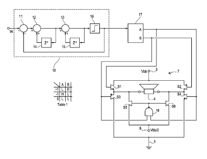
Figure 2 is a schematic showing a sigma-delta modulator 10, a decoder network
17 and an
controllable switch S5, and a sixth controllable switch S6. Also shown in
figure 2 is a table
illustrating the operation of the decoder network 17, denoted Table 1.
The input of the sigma-delta modulator 10 is connected to an output of a
digital signal
processor of a hearing aid (not shown), and the output of the sigma-delta
modulator 10 is
CA 02828263 2013-08-26
52966-92
9
The first supply voltage node 3 and the second supply voltage node 8 provides
electrical
power to the H-bridge output stage 7, and four of the eight controllable
switches, Si, S2, S3
and S4, are controlled by the decoder network 17 for controlling three
different conditions of
the output stage 7, denoted " ¨1", "0" and "+1", respectively. The NAND-gate
18 has a first
input connected to the first output A of the decoder network 17, and a second
input connected
to the second output B of the decoder network 17. The operation of the decoder
network 17 is
illustrated in Table 1, where L denotes a LOW logical level, and H denotes a
HIGH logical
level.
The first supply voltage node 3 preferably carries the nominal supply voltage
Vbb of the
hearing aid in order to maximize the output of the loudspeaker 4, but other
voltages may be
used for driving the loudspeaker 4, e.g. a voltage delivered by a voltage-
doubler being
powered by the battery of the hearing aid. The second supply voltage node 8
preferably
carries half the voltage of the first supply voltage node 3. The reasoning
behind this
preference will be explained in greater detail in the following.
The four controllable switches Si, S2, S3 and S4 operate in a fashion
generally similar to the
prior art output stage 1 shown in figure 1 regarding generation of the output
conditions " ¨ 1"
and "+l", but the output stage 7 has a novel way of generating the output
condition "0". The
NAND-gate 18 outputs a logical HIGH if, and only if, both the first output A
and the second
output B of the decoder network 17 are LOW. The two controllable switches S5
and S6 are
controlled by the NAND-gate 18.
When activated by a logical HIGH level, the fifth controllable switch S5
connects the first
loudspeaker terminal to the second supply node 8, and the sixth controllable
switch S6
connects the second loudspeaker terminal to the second supply node 8. When
deactivated by a
logical LOW level, the fifth controllable switch S5 and the sixth controllable
switch S6,
respectively, disconnects both the loudspeaker terminals from the second
supply node 8. In
other words, whenever the NAND-gate 18 outputs a logical HIGH, the first and
the second
loudspeaker terminal are both connected to the second supply node 8.
CA 02828263 2013-08-26
52966-92
If the voltage potential on the second supply voltage node 8 were configured
to equal either
the voltage potential on the first supply voltage node 3 or the ground
potential, the output
stage 7 would operate in essentially the same way as the output stage of the
prior art,
including the problems with capacitive interference discussed earlier.
However, if the voltage
In this configuration, the acoustic output transducer has an effective voltage
swing about the
potential Vbb/2 of the second voltage supply node 8 of the difference between
the ground
with respect to figures 3, 4 and 5, which are simplified schematic diagrams of
the output
stage 7 shown in figure 2, illustrating how the output stage 7 handles the
conditions " ¨1", "0"
and "+1". The first voltage supply node 3 and the second voltage supply node 8
are shown in
figure 3, figure 4 and figure 5. The six switches Si, S2, S3, S4, S5 and S6
are only suggested
In figure 3 it is illustrated how the output stage 7 generates the condition
"+1". The
switches Si and S4 are closed, while the switches S2, S3, SS and S6 are open.
Due to the
CA 02828263 2013-08-26
52966-92
11
voltage difference between the first supply voltage node 3 and ground, an
electrical current II
flows from the first supply voltage node 3 through Si, through the loudspeaker
4 and through
S4 to ground, exerting an electromotive force on the loudspeaker coil, thus
forcing the
membrane of the loudspeaker 4 to move in one direction, e.g. inwards.
In figure 4 is illustrated how the output stage 7 generates the condition "
¨1". The switches S2
and S3 are now closed, while the switches Si, S4, S5 and S6 are open. An
electrical current 12
flows from the first supply voltage node 3 through S2, through the loudspeaker
4 in the
opposite direction, and through S3 to ground, exerting an electromotive force
on the
loudspeaker coil, thus forcing the membrane of the loudspeaker 4 move in the
opposite
direction, e.g. outwards.
In figure 5 is illustrated how the output stage 7 generates the condition "0".
The switches S5
and S6 are now closed, while the switches Si, S2, S3 and S4 are open. The
voltage potential
of the second supply voltage node 8 is now applied on both terminals of the
loudspeaker 4
simultaneously. Unless the membrane of the loudspeaker 4 is at its resting
position, it is now
forced to move towards this resting position. This movement causes an
electrical current 13 to
flow in the closed circuit formed by the switch S5, the loudspeaker 4 and the
switch S6. As
the same voltage potential is applied to both terminals of the loudspeaker 4
by the second
supply voltage node 8, the current 13 originates solely from the electromotive
force induced in
the loudspeaker coil by the resilient force provided by the loudspeaker
suspension. When the
loudspeaker is in its resting position, and not in motion, the current 13 is
zero. By generating
the condition "0" in the three-level output converter of the invention in this
way, capacitive
interference is reduced.
The voltage potential provided by the second supply voltage node 8 may, in an
embodiment,
be generated by dividing the voltage potential of the first supply voltage
node 3 by two, e.g.
by providing a simple voltage divider having a sufficiently high output
impedance and
eventually being decoupled by a small capacitor. In another embodiment, a
switched-capacitor
voltage divider is provided for generating the voltage potential for the
second supply voltage
node 8 from the voltage potential of the first supply voltage node 3. A
switched-capacitor
CA 02828263 2013-08-26
52966-92
12
voltage divider is a choice in clocked, integrated circuit designs, and has
the added advantage
of having inherently high input impedance.
As stated in the foregoing, a three-level digital output stage has the
advantage of performing
fewer shifts for reproduction of the same signal when compared with a two-
level digital
converter according to the invention. The H-bridge output signal is a series
of equidistant,
clocked signal pulses representing the audio signal to be reproduced. This
signal may take one
of three distinct values, " ¨1", "0" or "+1". Also shown in the graph in
figure 6 is the resulting
loudspeaker movement. "+1" corresponds to the innermost extreme position
attainable by the
Figure 7 is a schematic of a hearing aid 20 having a digital output stage 7
according to the
invention. The hearing aid 20 comprises a microphone 21, an A/D converter 22,
a digital
signal processor 23, a sigma-delta converter 24, the output stage 7 and the
loudspeaker 4.
Acoustic signals are picked up by the microphone 21 and converted into an
analog electrical
CA 02828263 2013-08-26
52966-92
13
signal takes place in the hearing aid 20. From the output of the digital
signal processor 23, the
processed digital output signal is used as an input signal for the sigma-delta
converter 24.
The sigma-delta converter 24 uses the processed, digital output signal from
the digital signal
processor 23 as an input signal for generating a three-level bit stream
suitable as a digital
input signal for the H-bridge output stage 7. The H-bridge output stage 7 is
configured to
drive the loudspeaker 4 directly, controlled by the three-level bit stream.
The hearing aid
output stage according to the invention has significantly reduced capacitive
interference
without tradeoffs in the form of increased power consumption or added
complexity.