Note: Descriptions are shown in the official language in which they were submitted.
5-6 7-2- /
CA 02828396 2013-08-27
INDUCTION HEATING DEVICE
Technical Field
[0001] The present invention relates to an induction heating device
including a plurality of inverters, and having a control function to switch
and drive the respective inverters, individually.
Background Art
[0002] A conventional induction heating device will be described with
reference to the drawing.
[0003] Fig. 8 shows a circuit configuration of the conventional
induction heating device. In circuits shown in Fig. 8, a rectifying circuit
22 rectifies an AC power supply 21, and a smoothing circuit 23 smooths the
rectified output to obtain a DC power supply. An inverter 31a is carposed
of a heating coil 24a, a resonance capacitor 25a, and a switching element
26a. An inverter 31b is composed of a heating coil 24b, a resonance capacitor
25b, and a switching element 26b. An oscillating circuit 27a drives the
switching element 26a included in the inverter 31a. An oscillating circuit
27b drives the switching element 26b included in the inverter 31b. An input
current detecting circuit 28 detects a value of an input current, and a power
supply voltage detecting circuit 29 detects a voltage of the AC power supply.
A microcomputer 30 controls oscillations of the inverters 31a and 31b, based
on the values detected by the input current detecting circuit 28 and the
1
CA 02828396 2013-08-27
power supply voltage detecting circuit 29.
[0004] In the above configuration, the microcomputer 30 controls the
oscillating circuits 27a and 27b so that the oscillating circuits 27a and
27b are alternately driven. Further, the microcomputer 30 calculates a power
value based on a current value detected by the input current detecting circuit
28 and a voltage value detected by the power supply voltage detecting circuit
29 while controlling the oscillating circuit 27a, and uses the calculated
power value in correcting a power of the inverter 31a or the like. Similarly,
the microcorrputer 30 calculates a power value based on the current value
input by the input current detecting circuit 28 and the voltage value input
by the power supply voltage detecting circuit 29 while controlling the
oscillating circuit 27b, and uses the calculated power value in correcting
the power of the inverter 31b or the like (refer to patent document 1, for
example).
Prior Art Documents
Patent Documents
[0005]
Patent Document 1: JP 2001-196156 A
Surrunary of Invention
Problems to be Solved by the Invention
[0006] In the above-described induction heating device, it will be
considered a case in which, while the inverters 31a and 31b are intermittently
2
CA 02828396 2013-08-27
driven by the oscillating circuits 27a and 27b as described above, for
instance, alternately driven every half cycle, the inverter 31a outputs a
power of 2 kW, and the inverter 31b outputs a power of 1 kW, as one exarrple.
In this case, the inverter 31a needs to output a power of 4 kW in the half
cycle to output an average power of 2 kW. Similarly, the inverter 31b needs
to output a power of 2 kW in the half cycle to output an average power of
1 kW. Thus, every time the oscillating circuits 27a and 27b alternately drive
the inverters 31a and 31b every half cycle, the output power of the induction
heating device largely changes between 4 kW and 2 kW. Further, in a case
where the inverters 31a and 31b are driven so that the output power of the
induction heating device does not largely change even when the oscillating
circuits 27a and 27b are alternately driven, the output of the inverter
(either one of the inverters 31a and 31b) on which a small-diameter pan or
a non-magnetic stainless pan is put is reduced in some arts to protect the
switching elements when the small-diameter pan or the non-magnetic stainless
pan is heated. In this case also, the output power of the induction heating
device largely changes periodically. When such induction heating device is
used in a home, an AC voltage in the home changes in synchronization with
the output power of this induction heating device, and a lighting flicker
could be generated, for example.
[0007] In order
to solve the above conventional problem, the present
invention provides an induction heating device capable of preventing a
flicker phenomenon such as a flicker of a lighting equipment, caused by a
3
CA 02828396 2013-08-27
change of an output power generated due to alternate drive of two inverters.
Means for solving the problem
_ [0008] In order to solve the above conventional problem, an
induction
heating device according to the present invention includes a rectifying
circuit that rectifies an AC power supply; a smoothing capacitor that smooths
the rectified output to obtain a DC power supply; a first and a second
inverters each composed of a heating coil, a resonance capacitor, and a
switching element, and connected to the smoothing capacitor in parallel;
a first and a second oscillating circuits that supply drive signals to the
switching elements; and a controller that controls drive of the first and
second oscillating circuits. The controller alternately drives the first
and second oscillating circuits, and controls a drive time ratio of the first
and second oscillating circuits so that a power change amount generated every
time the drive is switched between the first and second oscillating circuits
is not more than a predetermined amount.
[0009] Further, when one output power of the first or second
inverter
is limited to a power smaller than a power required to obtain a set power,
the controller may limit the other output power of the first or second
inverter
so that a difference between the output power of the first inverter and the
output power of the second inverter is not more than the predetermined amount.
Effects of the Invention
[0010] According to the above configuration, the power change
amount
4
CA 02828396 2013-08-27
generated due to the alternate drive of the two inverters is reduced. As
a result, the flicker phenomenon (such as the flicker of the lighting
equipment) can be prevented from being generated, or kept at a level in which
a user does not feel strangeness.
Brief Description of Drawings
[0011] Fig. 1
is a view showing a circuit configuration of an induction
heating device according to a first or second embodiment of the present
invention.
Figs. 2A to 2G are views showing control timing of two
oscillating circuits according to the first or second embodiment of the
present invention.
Figs. 3A to 3G are views showing operations of switching
elements and an output power of the induction heating device when the two
oscillating circuits are alternately driven in a cycle of five ZVPs in the
first embodiment of the present invention.
Figs. 4A to 4G are views showing operations of switching
elements and an output power of the induction heating device when the two
oscillating circuits are alternately driven in a cycle of six ZVPs in the
first embodiment of the present invention.
Figs. 5A to 5E are views showing a change of the output power
of the induction heating device when set powers of the two inverters are
1.5 kW and 1 kW, respectively in the second embodiment of the present
CA 02828396 2013-08-27
invention.
Figs. 6A and 6E are views showing a change of the output power
_
of the induction heating device when a first inverter heats a small-diameter
pan or non-magnetic stainless pan in the second embodiment of the present
invention.
Figs. 7A to 7E are views showing a change of the output power
of the induction heating device when an output power of a second inverter
is limited based on a reference value of a power change in the second
embodiment of the present invention.
Fig. 8 is a view showing a circuit configuration of a
conventional induction heating device.
Mode for Carrying Out the Invention
[0012] An induction heating device according to a first
invention
includes a rectifying circuit that rectifies an AC power supply; a smoothing
capacitor that smooths the rectified output to obtain a DC power supply;
a first and a second inverters each composed of a heating coil, a resonance
capacitor, and a switching element, and connected to the smoothing capacitor
in parallel; a first and a second oscillating circuits that supply drive
signals to the switching elements; and a controller that controls drive of
the first and second oscillating circuits. The controller alternately
drives the first and second oscillating circuits, and controls a drive time
ratio of the first and second oscillating circuits so that a power change
6
CA 02828396 2013-08-27
amount generated every time the drive is switched between the first and second
oscillating circuits is not more than a predetermined amount. Thus, the
power change amount generated due to the alternate drive of the two inverters
can be limited. As a result, the flicker of the lighting equipment or the
like can be prevented from being generated, or kept at a level in which a
user does not feel strangeness.
[0013] According to an induction heating device in a second invention,
in the induction heating device according to the first invention especially,
the controller alternately drives the first and second oscillating circuits,
and when one output power of the first or second inverter is limited to a
power smaller than a power required to obtain a set power, the controller
reduces the other output power of the first or second inverter so that a
difference between the output power of the first inverter and the output
power of the second inverter is not more than the predetermined amount. Thus,
the power change amount generated due to the alternate drive of the two
inverters can be limited. As a result, the flicker of the lighting equipment
or the like can be prevented from being generated, or kept at the level in
which the user does not feel strangeness.
[0014] According to an induction heating device in a third invention,
in the induction heating device according to the first or second invention
especially, the predetermined amount is not more than a power amount
corresponding to a voltage change rate of the AC power supply in which a
short-time flicker value Pst is one. Thus, the power change amount generated
7
CA 02828396 2013-08-27
due to the alternate drive of the two inverters can be limited below or equal
to a border line whether people feel the flicker terrible. As a result, the
flicker of the lighting equipment or the like can be prevented from being
_
generated, or kept at the level in which the user does not feel strangeness.
[0015] According to an induction heating device in a fourth
invention,
in the induction heating device according to any one of the first to third
inventions especially, the controller performs control such that a cycle
time of the alternate drive of the first and second oscillating circuits
is not more than 300 milliseconds, and number of drive switching operations
between the first and second oscillating circuits per minute is not less
than 400. Thus, when the first and second oscillating circuits are
controlled by an intermittent operation in which heating and stopping are
alternately performed, an off-and-on boiling state which is likely to be
generated in an object to be heated particularly in boiling water or the
like can be kept at a level in which a user does not notice or does not feel
strangeness. As a result, the above state can be prevented from being falsely
recognized as a failure of an equipment.
[0016] According to an induction heating device in a fifth
invention,
in the induction heating device according to any one of the first to fourth
inventions especially, a zero-volt detecting circuit that detects a zero
point of the AC power supply is included. The controller switches the drive
between the first and second oscillating circuits, based on timing at which
the zero point of the AC power supply is detected by the zero-volt detecting
8
CA 02828396 2013-08-27
circuit. Thus, an instantaneous value of the AC power supply at the time
of switching the drive between the first and second oscillating circuits
is a lower voltage, compared with a time when the instantaneous value of
the AC power supply is high, so that a charge voltage to the smoothing
capacitor can be low. As a result, a rush current generated at the time of
an initial operation of each of the first and second inverters can be lowered,
so that an abnormal sound such as a pan rap or growl sound can be prevented
from being generated.
[0017] Hereinafter, embodiments of the present invention will be
described with reference to the drawings. Note that the present invention
is not limited to the embodiments.
[0018]
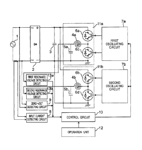
1. First Embodiment
1-1. Configuration of Induction Heating Device
Fig. 1 is a view showing a circuit configuration of an induction
heating device according to a first embodiment of the present invention.
[0019] As for circuits shown in Fig. 1, a rectifying circuit 2 is
a rectifying circuit that rectifies an AC power supply 1. A smoothing
capacitor 3 smooths the rectified output to obtain a DC power supply. A first
inverter lla is composed of a first heating coil 4a, a first resonance
capacitor Sa, and first switching elements 6a and 6c. A second inverter llb
is composed of a second heating coil 4b, a second resonance capacitor 5b,
and second switching elements 6b and 6d. The first and second inverters lla
9
CA 02828396 2013-08-27
and llb are connected to the smoothing capacitor 3 in parallel, and invert
the DC power supply to an alternate current. A first oscillating circuit
7a drives the first switching elements 6a and 6c in the first inverter lla.
A second oscillating circuit 7b drives the second switching elements 6b and
6d in the second inverter 11b. An input current detecting circuit 8 detects
a value of an input current. A zero-volt detecting circuit 9 detects a timing
(zero point) of positive and negative voltage inversion of an AC power supply
voltage. A first resonance voltage detecting circuit 13a detects a value
of a resonance voltage of the first resonance capacitor 5a. A second
resonance voltage detecting circuit 13b detects a value of a resonance
voltage of the second resonance capacitor 5b. An operation unit 12 receives
operations such as selection of heat / stop and a power adjustment (heating
power) for an object to be heated (cooking object) from a user. A control
circuit 10 includes a microcomputer. The control circuit 10 controls
oscillations of the first and second inverters lla and 11b, based on values
detected by the input current detecting circuit 8, the zero-volt detecting
circuit 9, and the first and second resonance voltage detecting circuits
13a and 13b, and a heat setting set in the operation unit 12. The induction
heating device (electromagnetic cooker represented by an TH cooking heater)
according to the present embodiment with the above configuration can
inductively heat objects to be heated such as a pan put on the first or second
heating coils 4a or 4b via a top panel, by an eddy current generated due
to magnetic coupling to the first and second heating coils 4a and 4b.
CA 02828396 2013-08-27
[0020] The control circuit 10 controls the first and second
oscillating circuits 7a and 7b so that each of the first and second inverters
lla and llb outputs a power corresponding to a heat power setting received
_
by the operation unit 12. Hereinafter, the output power of each of the first
and second inverters lla and llb corresponding to the heat power setting
set by the user is referred to as "set power".
[0021] Figs. 2A to 2G are views showing control timing of the
two
oscillating circuits 7a and 7b according to the present embodiment.
[0022] Referring to Fig. 2A indicates a voltage level of the
AC power
supply 1, Fig. 2B indicates a detection signal (output signal) of the
zero-volt detecting circuit 9, Figs. 2C and 2D indicate operation states
of the first and second oscillating circuits 7a and 7b, respectively, Figs.
2E and 2F indicate drive signals of the first and second switching elements
6a and 6b, respectively, and Fig. 2G indicates an output power of the
induction
heating device.
[0023] Note that each of the first switching elements 6a and
6c, and
the second switching elements 6b and 6d according to the present embodiment
is driven by a predetermined switching cycle (for example, high-frequency
cycle of 16 kHz or more which is not audible to the human ear) , regardless
of the set powers of the first and second inverters lla and 11b. An upper
limit of an on-time of each of the first and second switching elements 6a
and 6b is set to a half time of the switching cycle. Further, the first
switching element 6c and the second switching element 6d are exclusively
11
CA 02828396 2013-08-27
driven with respect to the first switching element 6a and the second switching
element 6b, respectively. Thus, a lower limit of an on-time of each of the
first and second switching elements 6c and 6d is the half time of the
switching
cycle. Therefore, when the on-time of each of the first switching elements
6a and 6c and the second switching elements 6b and 6d is the half of the
switching cycle, the output power of each of the inverters lla and llb is
maximum.
[0024]
1-2. Operation of Induction Heating Device
Hereinafter, an operation and a mechanism of the induction
heating device configured as described above will be described.
[0025]
1-2-1. Outline of Operation
First, a description will be given of an outline of switching
timing between the first and second oscillating circuits 7a and 7b, and
operation timing of the first switching elements 6a and 6c and the second
switching elements 6b and 6d.
[0026] When the
heating operation of the first and second inverters
lla and 11b is selected in the operation unit 12, the control circuit 10
which received the signal from the operation unit 12 starts to send respective
control signals to the first and second oscillating circuits 7a and 7b so
that the first and second oscillating circuits 7a and 7b drive the first
switching elements 6a and 6c, and the second switching elements 6b and 6d.
12
CA 02828396 2013-08-27
[0027] As shown in Fig. 2C, a drive period of the first oscillating
circuit 7a by the control circuit 10 is a period Tl. As shown in Fig. 2D,
a drive period of the second oscillating circuit 7b is a period T2. As shown
in Fig. 2E, the first switching elements 6a and 6c are driven by the first
oscillating circuit 7a in the period Tl, according to the above-described
predetermined switching cycle which is shorter than the periods T1 and T2.
As shown in Fig. 2F, the second switching elements 6b and 6d are driven by
the second oscillating circuit 7b in the period T2, according to the
above-described predetermined switching cycle which is shorter than the
periods T1 and T2. That is, the first and second oscillating circuits 7a
and 7b are operated intermittently in the periods T1 and T2, respectively,
and alternately in a predetermined cycle T (T1 + T2) . Thus, the first
switching elements 6a and 6c and the second switching elements 6b and 6d
are also driven intermittently in the periods T1 and T2, respectively, and
alternately in the predetermined cycle T, according to the predetermined
switching cycle which is shorter than the periods T1 and T2.
[0028] A description will be given of the timing to switch the
operation between the first and second oscillating circuits 7a and 7b by
the control circuit 10. As shown in Figs. 2A and 2B, the zero-volt detecting
circuit 9 outputs a high-level signal when a voltage level of the AC power
supply 1 is in a positive side, and outputs a low-level signal when the
voltage
level of the AC power supply 1 is on a negative side. Then, the zero-volt
detecting circuit 9 outputs a falling edge from the high level to the low
13
CA 02828396 2013-08-27
level and a rising edge from the low level to the high level when the voltage
level of the AC power supply 1 is in the vicinity of a zero point. Therefore,
the detection signal (output signal) of the zero-volt detecting circuit 9
is a pulse signal of the cycle of the AC power supply.
[0029] The control circuit 10 detects the zero point of the AC power
supply 1 with the output signal of the zero-volt detecting circuit 9, and
switches the operation between the first and second oscillating circuits
7a and 7b in the vicinity of the zero point of the AC power supply 1. For
exatrple, in the case where the operation is switched from the first
oscillating circuit 7a to the second oscillating circuit 7b, when the
zero-volt detecting circuit 9 outputs the rising or falling edge, the control
circuit 10 stops the operation of the first operating oscillating circuit
7a in operation at first and then starts the operation of the second
oscillating circuit 7b. That is, when the voltage level of the AC power supply
1 reaches the zero point, the operation of the first oscillating circuit
7a is stopped, and after a time of the zero point, the operation of the second
oscillating circuit 7b is started. The same is true for the switching from
the operation of the second oscillating circuit 7b to the operation of the
first oscillating circuit 7a.
[0030] Further, since the operations between the first and second
oscillating circuits 7a and 7b are switched in the vicinity of the zero point
of the AC power supply 1, the operation period T1 of the first oscillating
circuit 7a and the operation period T2 of the second oscillating circuit
14
CA 02828396 2013-08-27
7b are set in units of the half cycle of the AC power supply cycle (that
is, each of the operation period T1 of the first oscillating circuit 7a and
the operation period T2 of the second oscillating circuit 7b is set to the
integral multiple of the half cycle of the AC power supply cycle) .
Hereinafter, a length of the half of the AC power supply cycle is referred
to as "ZVP (zero volt pulse)". As shown in Figs. 23 to 2D, the period T1
corresponds to three pulses of the ZVP (three ZVPs) , and the period T2
corresponds to two pulses of the ZVP (two ZVPs) . Thus, the first and second
oscillating circuits 7a and 7b are alternately operated in a cycle of five
ZVPs.
[0031] When the
first and second oscillating circuits 7a and 7b are
operated in this way, as shown in Fig. 2G, the output power of the induction
heating device is an output power P1 from the first inverter lla in the period
Tl, and is an output power P2 from the second inverter llb in the period
T2. Therefore, the output power of the induction heating device changes
between the output power P1 and the output power P2 every time the first
and second oscillating circuits 7a and 7b are alternately operated. Since
the intermittent operation is performed such that the first inverter lla
is operated in the three ZVPs of the cycle of five ZVPs, the output power
for one cycle of the induction heating device from the first inverter 11a
is an average power of 3 / 5 time of the output power Pl. Further, since
the intermittent operation is performed such that the second inverter llb
is operated in the two ZVPs of the cycle of five ZVPs, the output power for
CA 02828396 2013-08-27
one cycle of the induction heating device from the second inverter llb is
an average power of 2 / 5 time of the output power P2.
[0032]
_
1-2-2. Operation to Determine Switching Cycle of Oscillating Circuit
Next, a description will be given of a case in which the set
powers of the first and second inverters lla and llb are both set to 1 kW,
with reference to Figs. 3A to 3G and Figs. 4A and 4G. Fig. 3A to 3G are views
showing operations of switching elements and an output power of the induction
heating device when the two oscillating circuits according to the present
embodiment are alternately driven in the cycle of five ZVPs. Figs. 4A and
4G are views showing operations of switching elements and an output power
of the induction heating device, when the two oscillating circuits according
to the present embodiment are alternately driven in a cycle of six ZVPs.
[0033] Referring to Figs. 3A to 3G and Fig. 4A and 4G, Figs.
3A and
4A indicate a voltage level of the AC power supply, Figs. 3B and 4B indicate
a detection signal (output signal) of the zero-volt detecting circuit 9,
Figs. 3C and 4C, and 3D and 4D indicate operation states of the first and
second oscillating circuits 7a and 7b, respectively, Figs. 3E and 4E, and
3F and 4F indicate drive signals of the first and second switching elements
6a and 6b, respectively, and Figs. 3G and 4G indicate an output power of
the induction heating device.
[0034] As described above, the first and second oscillating
circuits
7a and 7b are operated intermittently in the periods T1 and T2, respectively,
16
CA 02828396 2013-08-27
and alternately in the predetermined cycle T. The control circuit 10
controls the first and second oscillating circuits 7a and 7b so that the
first and second inverters lla and llb are operated in the cycle of five
ZVPs or six ZVPs, regardless of the set power of each of the first and second
inverters lla and 11b. Further, the periods T1 and T2 are changed based on
the set power of each of the first and second inverters lla and 11b.
[0035] The cycle T needs to be determined so that a time for one cycle
is 300 milliseconds or less, and number of the switching operations between
the first and second oscillating circuits 7a and 7b per minute is 400 or
more. The purpose of determining the cycle T as described above is to control
a degree of an off-and-on boiling state which is likely to be generated in
the object to be heated in boiling water or the like especially, while the
induction heating device performs the intermittent operation in which the
heating operation and the stop are alternately performed.
[0036] Hereinafter, a concrete method for determining the cycle T
will be described. Here, a frequency of the AC power supply 1 is 50 Hz or
60 Hz. Therefore, length of the half cycle (ZVP) of the output of the AC
power supply 1 is 10 milliseconds when the frequency is 50 Hz, and is 8.3
milliseconds when the frequency is 60 Hz. Therefore, the cycle T of five
ZVPs is 50 milliseconds when the frequency is 50 Hz, and is 42 milliseconds
when the frequency is 60 Hz. Further, the cycle T of six ZVPs is 60
milliseconds when the frequency is 50 Hz, and is 50 milliseconds when the
frequency is 60 Hz. Therefore, both of the cycle T of six ZVPs and the cycle
17
CA 02828396 2013-08-27
T of five ZVPs satisfies the above condition. The same is true for the number
of the switching operations between the first and second oscillating circuits
7a and 7b per minute. When the fact that the two switching operations are
generated every cycle is taken into account, the number of the switching
operations per minute in the case where the cycle T is five ZVPs is 2400
when the frequency is 50 Hz, and is 2880 when the frequency is 60 Hz. Further,
the number of the switching operations per minute in the case where the cycle
is six ZVPs is 2000 when the frequency is 50 Hz, and is 2400 when the
frequency
is 60 Hz. Thus, as for the number of the switching operations per minute
also, both of the cycle T of five ZVPs and cycle T of six ZVPs satisfies
the condition.
[0037] Note that the cycle T is not limited to five ZVPs and six ZVPs,
and there is no problem even when the cycle T is set to any value except
for five ZVPs and six ZVPs as long as the above-described condition is
satisfied. Since the time of the one cycle is set to 300 milliseconds or
less, the cycle T can be set to any value within a range of up to 30 ZVPs
when the frequency of the AC power supply 1 is 50 Hz, and the cycle T can
be set to any value within a range of up to 36 ZVPs when the frequency of
the AC power supply 1 is 60 Hz,
[0038] The periods Tl and T2 are determined as follows. The operation
period T1 of the first oscillating circuit 7a is calculated based on a
following formula.
[0039]
18
CA 02828396 2013-08-27
(Period T1) = (cycle T) x (set power of first inverter 11a)
/ (total of set powers of first and second inverters lla and 11b)
[0040] Since the periods T1 and T2 are determined with the half cycle
of the AC power supply using as the minimum unit as described above, when
the calculation result is indivisible, the calculation result is rounded
off to the whole number. The operation period T2 of the second oscillating
circuit 7b is calculated based on a following formula.
[0041]
(Period T2) = (cycle T) - (period T1)
[0042] In the above configuration, first, a description will be given
of the case where the first and second oscillating circuits 7a and 7b are
alternately operated in the cycle of five ZVPs, with reference to Figs. 3A
to 3G. When the set powers of the first and second inverters lla and llb
are both set to 1 kW, the total of the set powers is 2 kW. Therefore, the
operation periods T1 and T2 of the first and second oscillating circuits
7a and 7b are calculated such that T1 = three ZVPs and T2 = two ZVPs, based
on the above formulas, respectively. Since the intermittent operation is
performed such that the first inverter lla is operated in the period of three
ZVPs of the cycle of five ZVPs, and the average of the output power in the
cycle T (that is, the set power) of the first inverter lla is 1 kW, the output
power needs to be 5 / 3 times the set power. Therefore, the output power
of the first inverter lla needs to be 1.7 kW in the period T1. Further, since
the intermittent operation is performed such that the second inverter lib
19
CA 02828396 2013-08-27
is operated in the period of two ZVPs of the cycle of five ZVPs, and the
average of the output power in the cycle T (that is, the set power) of the
second inverter llb is 1 kW, the output power needs to be 5 / 2 times the
_
set power. Therefore, the output power of the second inverter llb needs to
be 2.5 kW in the period T2. Therefore, as shown in Fig. 3G, the output power
of the induction heating device changes between 1.7 kW and 2.5 kW every time
the first and second oscillating circuits 7a and 7b are alternately operated
in the cycle of five ZVPs. Hereinafter, a difference between the output power
of the first inverter lla in the period T1 and the output power of the second
inverter llb in the period T2 is referred to as "power change amount". The
power change amount in this case is 800 W (2.5 kW - 1.7 kW) .
[0043]
Next, a description will be given of the case where the first
and second oscillating circuits 7a and 7b are alternately operated in the
cycle of six ZVPs, with reference to Figs. 4A to 4G. The operation periods
T1 and T2 of the first and second oscillating circuits 7a and 7b are
calculated
such that T1 = three ZVPs and T2 = three ZVPs, based on the above formulas,
respectively. Since the intermittent operation is performed such that the
first inverter lla is operated in the period of three ZVPs of the cycle of
six ZVPs, and the average of the output power of the first inverter lla is
1 kW in the cycle T, the output power needs to be 6 / 3 times the set power.
Therefore, the output power of the first inverter lla needs to be 2 kW in
the period T1. The output power of the second inverter llb is similarly
calculated. Since the intermittent operation is performed such that the
CA 02828396 2013-08-27
second inverter llb is operated in the period of three ZVPs of the cycle
of six ZVPs, the output power of the second inverter llb needs to be 2 kW
in the period T2. Therefore, as shown in Fig. 4E, the output power of the
induction heating device is constant at 2 kW while the first and second
oscillating circuits 7a and 7b are alternately operated in the cycle of six
ZVPs. That is, the power change amount in this case is zero W.
[0044] According to the present embodiment, the control circuit 10
sets the cycle T to five ZVPs or six ZVPs, based on whether the power change
amount generated when the first and second oscillating circuits 7a and 7b
are switched is a reference amount or lower. That is, the control circuit
alternately drives the first and second oscillating circuits 7a and 7b,
and controls a drive time ratio (T1 : T2) of the first and second oscillating
circuits 7a and 7b so that the power change amount generated every time the
drive is switched between the first and second oscillating circuits 7a and
7b is the reference amount or less. As a result, a flicker phenomenon such
as a flicker of a lighting equipment can be prevented.
[0045] Here, the "reference amount" for the power change amount used
in determining the cycle T is previously determined, in view of a flicker
of a light caused by the power change generated when the first and second
oscillating circuits 7a and 7b are switched. For example, the reference
amount is determined as a maximum amount in a range of the power change amount
which corresponds to a flicker whose degree is not felt terrible to the human
eyes.
21
CA 02828396 2013-08-27
[0046] According to the present embodiment, a short-time flicker
indicator is used as an index to determine this reference amount.
[0047] Hereinafter, a specific description will be given of the
reference amount for the power change amount used in determining the cycle
T. When an equipment having a relatively high load such as the induction
heating device or the like is operated, a light such as an incandescent lamp
is dimmed in some cases. This is because a large current flows due to the
operation of the equipment and thus the AC power supply voltage is lowered.
To prevent such flicker of the light, there is an international standard
to limit the change in the current consumption of an equipment.
Particularly, there is an index called the short-time flicker indicator Pst
in which severity of the flicker is quantified based on characteristics of
the human eyes. The short-time flicker indicator Pst is a graph in which
a border line indicating whether the human feels the flicker terrible is
defined as one. In general, the abscissa axis of the graph of the short-time
flicker indicator Pst indicates number of step-shaped voltage changes per
minute, and the ordinate axis indicates a magnitude of a voltage change when
a rated voltage is set to 100%. When the AC power supply 1 according to the
present embodiment is 240 V / 50 Hz, and the cycle T is five ZVPs, the number
of the switching operations between the first and second oscillating circuits
7a and 7b per minute is 2400, as described above. Thus, the number of the
voltage changes is also 2400. Here, according to the short-time flicker
indicator Pst, when the number of the voltage changes per minute is 2400,
22
CA 02828396 2013-08-27
the magnitude of the voltage change on the border line (Pst = 1) is 0.75 96.
Therefore, the power change amount corresponding to the magnitude of the
voltage change of 0.75 96 which satisfies that Pst = 1 is calculated from
impedance Zref = 0.47 f2 (= 0.4 SI + jn 0.25 12) to be about 920 W through
a following calculation.
[0048]
(Voltage change amount) = (rated voltage) x (magnitude of
voltage change satisfying that Pst = 1) = 240 (V) x 0.75 (%) / 100 = 1.8
On
(Current change amount) = (voltage change amount) / Zref =
1.8 Op / 0.47 (12) = 3.83 (IQ
(Power change amount) = (rated voltage) x (current change
amount) = 240 On x 3.83 (I) = 919 (W)
[0049] The
power change amount which satisfies that Pst = 1 in the
case where the cycle T is six ZVPs is similarly calculated. When the cycle
T is six ZVPs, the number of the switching operations between the first and
second oscillating circuits 7a and 7bperminute is 2000, and thus the voltage
change number is also 2000. Further, according to the short-time flicker
indicator Pst, the magnitude of the voltage change on the border line (Pst
= 1) is 0.5 %. Therefore, the power change amount which satisfies that Pst
= 1 is calculated to be about 610 W. The reference amount is set to be not
more than the power change amount calculated based on the flicker indicator
Pst in each of the cases where the cycle T is five ZVPs and six ZVPs. In
23
CA 02828396 2013-08-27
the present embodiment, in each of the cases where the cycle T is five ZVPs
and six ZVPs, the reference amount is set to a value of 70 % of the calculated
power change amount. Therefore, when the cycle T is five ZVPs, the reference
amount is set to about 650 W, and when the cycle T is six ZVPs, the reference
amount is set to about 430 W. Note that, the reference amount is set to 70 %
of the calculated power change amount in the present embodiment, but the
present invention is not limited to this embodiment. The same effect can
be provided as long as the reference amount is set to an allowable power
change amount (power change amount satisfying Pst = 1) or less.
[0050] As
described above, when the first and second oscillating
circuits 7a and 7b are alternately operated in the cycle of five ZVPs, the
output power of the induction heating device changes between 1.7 kW and 2.5
kW, and thus the power change amount is 800 W. Further, when the cycle T
is six ZVPs, the output power is constant at 2 kW, and thus the power change
amount is zero W. When these power change amounts are cotrpared with the above
reference amount, the power change in the operation of the induction heating
device in the cycle of five ZVPs exceeds the reference value, and the power
change in the operation of the induction heating device in the cycle of six
ZVPs is not more than the reference amount. Therefore, the control circuit
determines that the alternate operations of the first and second
oscillating circuits 7a and 7b in the cycle of six ZVPs in which the power
change is not more than the reference amount are approved, and that the
alternate operations in the cycle of five ZVPs in which the power change
24
CA 02828396 2013-08-27
exceeds the reference amount are disapproved.
[0051] Note that, depending on the set powers of the first and second
inverters lla and 11b, the power change amount in the operation in the cycle
of five ZVPs and the power change amount in the operation in the cycle of
six ZVPs are both not more than the reference amount. In this case, there
is no problem in suppressing the flicker of the light or the like in each
operation. Thus, in the present embodiment, the induction heating device
is operated in the cycle T in which the power change amount is smaller.
Further, in the present embodiment, the set power is provided so that the
power change amount is surely the reference amount or less, in either or
both of the operations in the cycle of five ZVPs and in the cycle of six
ZVPs, in all possible combinations of the set powers of the first and second
inverters lla and llb . Therefore, a case where both of the power change
amount
in the operation in the cycle of five ZVPs and the power change amount in
the operation in the cycle of six ZVPs exceed the reference amount does not
occur.
[0052] Further, in the present embodiment, to control the drive time
ratio (T1 : T2) of the first and second oscillating circuits 7a and 7b, the
drive cycle T of the first and second oscillating circuits 7a and 7b is
adjusted. However, the present invention is not limited to this. The drive
times T1 and T2 may be adjusted while the cycle T is fixed.
[0053]
1-3. Conclusion of the Present Embodiment
CA 02828396 2013-08-27
As described above, the induction heating device according
to the present embodiment includes the rectifying circuit 2 that rectifies
an AC power supply; the smoothing capacitor 3 that smooths the rectified
output to obtain a DC power supply; the first and a second inverters that
invert the DC power supply to an alternate current by the first and second
switching elements 6a, 6c, 6b, and 6d to supply high-frequency power, and
connected to the smoothing capacitor 3 in parallel; the first and a second
oscillating circuits 7a and 7b that supply drive signals to the switching
elements 6a, 6c, 6b, and 6d in the first and a second inverters lla and llb;
and a control circuit 10 that controls the drive of the first and second
oscillating circuits . The controller alternately drives the first and
second oscillating circuits 7a and 7b, and controls a drive time ratio of
the first and second oscillating circuits 7a and 7b so that a power change
amount generated every time the drive is switched between the first and second
oscillating circuits 7a and 7b is not more than the reference amount. As
a result, the power change amount generated due to the alternate drives of
the two first and second inverters lla and llb can be suppressed. Thus, the
flicker of the lighting equipment can be prevented from being generated,
or controlled to the level in which the user does not feel strangeness.
[0054] Further,
according to the induction heating device in the
present embodiment, the power change amount generated every time the drive
is switched between the first and second oscillating circuits 7a and 7b can
be equal to or less than the power change amount corresponding to a voltage
26
CA 02828396 2013-08-27
change rate of the AC power supply in which the short-time flicker value
Pst is one. Thus, the power change amount generated due to the alternate
drive of the two first and second inverters lla and llb can be equal to or
less the border line whether people feel the flicker terrible. As a result,
the flicker of the lighting equipment or the like can be prevented from being
generated, or kept at the level in which the user does not feel strangeness.
[0055] Further, according to the induction heating device in the
present embodiment, the cycle time T of the alternate drive of the first
and second oscillating circuits 7a and 7b can be set to 300 milliseconds
or less, and the number of the drive switching operations per minute can
be set to 400 or more. As a result, during the intermittent operation in
which the heating operation and the stop are alternately performed, the
induction heating device can keep a degree of an off-and-on boiling state
which is likely to be generated in the object to be heated particularly in
boiling water or the like, at a level in which the user does not notice or
does not feel strangeness. Thus, the user can be prevented from mistaking
the intermittent boiling state for a defect of the equipment or the like.
[0056] Furthermore, the induction heating device according to the
present embodiment includes the zero-volt detecting circuit 9 that detects
the zero point of the AC power supply 1. The control circuit 10 switches
the drive between the first and second oscillating circuits 7a and 7b, in
the vicinity of the zero point of the AC power supply detected by the zero-
volt
detecting circuit 9. As a result, an instantaneous value of the AC power
27
CA 02828396 2013-08-27
supply 1 at the time of switching the drive between the first and second
oscillating circuits 7a and 7b is a voltage lower than the maxitra.un value
of the instantaneous value of the AC power supply 1, and thus a charge voltage
to the smoothing capacitor 3 can be kept low. Therefore, an inrush current
generated at the time of an initial operation of each of the first and second
inverters lla and llb can be kept low, and thus an abnormal sound such as
a pan rap or growl sound can be prevented from being generated.
[0057]
2. Second Embodiment
Hereinafter, a second embodiment of the present invention will
be described. Because a basic configuration of an induction heating device
according to the present embodiment is the same as the configuration of the
induction heating device according to the first embodiment, the same
component is marked with the same reference sign, and its description is
omitted. Further, because a basic operation of the induction heating device
according to the present embodiment is the same as the operation of the
induction heating device according to the first embodiment, its description
is omitted.
[0058] As shown
in Fig. 2G, in the induction heating device according
to the present embodiment, the first inverter lla outputs the power P1 in
the period Tl, and the second inverter llb outputs the power P2 in the period
T2. The output power of the induction heating device changes between the
powers P1 and P2 every time the first and second oscillating circuits 7a
28
CA 02828396 2013-08-27
and 7b are alternately operated. Since intermittent operation is performed
such that the first inverter lla is operated in the period of three ZVPs
of the cycle of five ZVPs, the first inverter lla outputs the average power
of 3 / 5 time of the output power P1, in the cycle T. Further, since the
intermittent operation is performed such that the second inverter llb is
operated in the period of two ZVPs of the cycle of five ZVPs, the second
inverter llb outputs the average power of 2 / 5 time of the output power
P2, in the cycle T.
[0059]
Hereinafter, a description will be given of an operation of
the induction heating device according to the present embodiment performed
when either one of the output powers of the first and second inverters lla
and llb is limited. First, a description will be given of a case where either
one of the output powers of the first and second inverters lla and llb is
not limited, and then a description will be given of the case where the output
power is limited.
[0060]
2-1. Operation When Output Power of Inverter Is Not Limited
A description will be given of a case where the set powers
of the first and second inverters lla and llb are 1.5 kW and 1 kW,
respectively,
with reference to Figs. 5A to 5E. Figs. 5A to 5E are views showing a change
of the output power of the induction heating device generated when the set
powers of the two inverters are 1.5 kW and 1 kW, respectively in this
embodiment.
29
CA 02828396 2013-08-27
[0061] Referring to Figs. 5A to 5E, Fig. 5A indicates a voltage level
of the AC power supply 1, Fig. 5B indicates a detection signal (output signal)
of the zero-volt detecting circuit 9, Figs. SC and SD indicate operation
states of the first and second oscillating circuits 7a and 7b, respectively,
and Figs. 5E indicates an output power of the induction heating device.
[0062] As described above, the control circuit 10 controls the first
and second oscillating circuits 7a and 7b so that the first and second
oscillating circuits 7a and 7b are operated intermittently in the periods
T1 and T2, respectively and alternately in the cycle of five ZVPs . The
periods
T1 and T2 are determined based on the respective set powers of the first
and second inverters lla and 11b. The determination method is as follows
similar to the first embodiment. The operation period T1 of the first
oscillating circuit 7a is calculated based on a following formula.
[0063]
(Period T1) = (cycle T) x (set power of first inverter 11a)
/ (total of set powers of first and second inverters lla and 11b)
[0064] Since lengths of the periods T1 and T2 are determined with
the half cycle of the AC power supply using as the minimum unit, when the
calculation result is indivisible, the calculation result is rounded off
to the whole number. The operation period T2 of the second oscillating
circuit 7b is calculated based on a following formula.
[0065]
(Period T2) = (cycle T) - (period T1)
CA 02828396 2013-08-27
[0066] When
the set powers of the first and second inverters lla and
llb are respectively selected as 1.5 kW and 1 kW, the total of the set powers
is 2.5 kW. Therefore, the operation periods T1 and T2 of the first and second
oscillating circuits 7a and 7b are respectively calculated such that T1 =
three ZVPs, and T2 = two ZVPs. Since the intermittent operation is performed
such that the first inverter lla is operated in the period of three ZVPs
of the cycle of five ZVPs, in order that the first inverter lla outputs the
average power of 1.5 kW in the cycle T, the first inverter lla needs to output
a power of 5 / 3 times the set power in the period T1. Thus, the output power
of the first inverter lla is 2.5 kW in the period T1. Further, since the
intermittent operation is performed such that the second inverter llb is
operated in the period of two ZVPs of the cycle of five ZVPs, in order that
the second inverter llb outputs the average power of 1 kW in the cycle T,
the second inverter llb needs to output a power of 5 / 2 times the set power
in the period T2. Thus, the output power of the second inverter llb is 2.5
kW in the period T2. Therefore, as shown in Fig. 5E, in the case where the
set powers of the first and second inverters lla and llb are respectively
set to 1.5 kW and 1 kW, even when the first and second oscillating circuits
7a and 7b are alternately operated, the output power of the induction heating
device is constant at 2.5 kW.
[0067]
2-2. Operation in Case Where Output Power of Inverter Is Limited
Next, a description will be given of a case where the set powers
31
CA 02828396 2013-08-27
of the first and second inverters lla and llb are respectively selected as
1.5 kW and 1 kW, and the first inverter lla is operated under a condition
that a small-diameter pan or non-magnetic stainless pan is put on the first
heating coil 4a, with reference to Figs. 6A to 6E and Figs. 7A to 7E. Figs.
6A to 6E are views showing a change of the output power of the induction
heating device when the first inverter lla according to the present
embodiment heats the small-diameter pan or the non-magnetic stainless pan.
Fig. 7A to 7E are views showing a change of the output power of the induction
heating device when the output power of the second inverter llb is limited,
based on a reference value of the power change according to the present
embodiment.
[0068] When the
small-diameter pan or the non-magnetic stainless pas
is heated, a resonant current flowing in each of the first switching elements
6a and 6c, and the second switching elements 6b and 6d is larger, conpared
with a case where an iron pan such as a porcelain-clad pan is heated. Thus,
depending on the output power, the switching element could be broken. To
prevent the switching element from being broken, the induction heating device
according to the present embodiment includes a protecting means that prevents
the resonant current flowing in each of the first switching elements 6a and
6c and the second switching element 6b and 6d from reaching a predetermined
amount or more. That is, the induction heating device detects values of the
resonance voltages generated in the first and second resonance capacitors
5a and 5b by the first and second resonance voltage detecting circuits 13a
32
CA 02828396 2013-08-27
and 13b to limit the output powers of the first and second inverters 11a
and 11b.
[0069] For example, a case where the first switching elements 6a and
6c and the second switching elements 6b and 6d could be broken when the output
powers of the first and second inverters lla and llb are 1.5 kW or more will
be considered. In this case, as shown in Figs. 6A to 6E, the output power
of the first inverter lla is limited to 1.5 kW in the period Tl, instead
of original 2.5 kW. Thus, as shown in Fig. 6E, the output power of the
induction heating device changes between 1.5 kW and 2.5 kW every time the
first and second oscillating circuits 7a and 7b are alternately operated.
[0070] Note that the output powers of the first and second inverters
lla and llb are limited by reducing duty ratios in switching the first
switching elements 6a and 6c and the second switching elements 6b and 6d.
[0071] When the change amount of the output power of the induction
heating device exceeds the reference amount due to the limitation of the
output power of the first inverter 11a, the control circuit 10 limits the
output power of the second inverter llb so that the power change amount is
the reference amount or less. Here, the reference amount is previously
determined similar to the first embodiment.
[0072] Hereinafter, a specific description will be given of the
reference amount for the power change amount used in limiting the output
power of the second inverter 11b. When an equipment having a relatively high
load such as the induction heating device or the like is operated, a light
33
CA 02828396 2013-08-27
such as an incandescent lamp is dimmed in some cases. This is because a large
current flows due to the operation of the equipment and thus the AC power
supply voltage is lowered. To prevent such flicker of the light, there is
an international standard to limit the change in the current consumption
of an equipment. Particularly, there is an index called the short-time
flicker indicator Pst in which severity of the flicker is quantified based
on characteristics of the human eyes. The short-time flicker indicator Pst
is a graph in which a border line indicating whether the human feels the
flicker terrible is defined as one. In general, the abscissa axis of the
graph of the short-time flicker indicator Pst indicates number of step-shaped
voltage changes per minute, and the ordinate axis indicates a magnitude of
a voltage change in percent of a rated voltage. When the AC power supply
1 according to the present embodiment is 240 V / 50 Hz, and the cycle T is
five ZVPs, the number of the switching operations between the first and second
oscillating circuits 7a and 7b per minute is 2400, as described above. Thus,
the number of the voltage changes is also 2400. Here, according to the
short-time flicker indicator Pst, when the number of the voltage changes
per minute is 2400, the magnitude of the voltage change on the border line
(Pst = 1) is 0.75 %. Therefore, the power change amount corresponding to
the magnitude of the voltage change of 0.75 % which satisfies that Pst =
1 is calculated from impedance Zref = 0.47 û (= 0.4 in 0.25
K-2) to be
about 900 W through a following calculation.
[0073]
34
CA 02828396 2013-08-27
(Voltage change amount) = (rated voltage) x (magnitude of
voltage change satisfying that Pst = 1) = 240 (7) x 0.75 (%) / 100 = 1.8
(7)
(Current change amount) = (voltage change amount) / Zref =
1.8 Ofl / 0.47 (Q) = 3.83 (IQ
(Power change amount) = (rated voltage) x (current change
amount) = 240 Ofl x 3.83 (1)0 = 919 0,0
[0074] The reference amount is set to be not more than the calculated
power change amount. In the present embodiment, the reference amount is set
to a value of about 50 96 of the calculated power change amount. Thus, the
reference amount is set to 400 W. Note that, the reference amount is set
to 50 96 of the calculated power change amount in the present embodiment,
but the present invention is not limited to this embodiment. The same effect
can be provided as long as the reference amount is set to an allowable power
change amount (power change amount satisfying Pst = 1) or less.
[0075] Based on the reference amount (400 W) set as described above,
and the output power (1.5 kW) of the first inverter lla, a maximum value
which can be set as the output power of the second inverter llb is determined
as 1.9 kW (1.5 kW + 0.4 kW) . Thus, the control circuit 10 limits the output
power of the second inverter 11b to 1.9 kW, and alternately operates the
first and second inverters lla and 11b. As a result, as shown in Fig. 7E,
the output power of the induction heating device changes between 1.5 kW and
1.9 kW every time the first and second oscillating circuits 7a and 7b are
CA 02828396 2013-08-27
alternately operated. Therefore, the power change amount is reduced from
1000 W (2.5 kW - 1.5 kW) to 400W (1.9 kW - 1.5 kW) which is not more than
the reference amount.
[0076] Note
that, the present embodiment discloses the means for
detecting the values of the resonance voltages generated in the first and
second resonance capacitors 5a and 5b as the means for protecting the first
switching elements 6a and 6c and the second switching elements 6b and 6d,
but the present invention is not limited to this means. A current transformer
or the like may be provided in a current path of the resonant current, and
thereby the values of the currents flowing in the first switching elements
6a and 6c and the second switching elements 6b and 6d may be directly
detected.
The same effect can be also provided by this means, as a matter of course.
[0077]
2-3. Conclusion of the Present Embodiment
As described above, the induction heating device according
to the present embodiment includes the rectifying circuit 2 that rectifies
an AC power supply 1; the smoothing capacitor 3 that smooths the rectified
output to obtain a DC power supply; the first and second inverters lla and
11b composed of the first and second heating coils 4a and 4b, the first and
second resonance capacitors 5a and 5b, and the first switching elements 6a
and 6c and the second switching elements 6b and 6d, and connected to the
smoothing capacitor 3 in parallel; the first and second oscillating circuits
7a and 7b that supply the drive signals to the first switching elements 6a
36
CA 02828396 2013-08-27
and 6c, and the second switching elements 6b and 6d; and the control circuit
that controls the drive of the first and second oscillating circuits 7a
and 7b. The control circuit 10 alternately drives the first and second
oscillating circuits 7a and 7b, and when one output power of the first or
second inverter lla or llb is limited to a power smaller than a power required
to obtain a set power, the control circuit 10 limits the other output power
of the first or second inverter lla or llb so that a difference between the
output power of the first inverter lla and the output power of the second
inverter llb is not more than the predetermined amount. As a result, the
flicker of the lighting equipment or the like can be prevented from being
generated, or kept at the level in which the user does not feel strangeness.
[0078] Further, the induction heating device according to the present
embodiment, similarly to the first embodiment, makes a difference between
the output powers of the first and second inverters lla and llb into a power
amount corresponding to a voltage change rate of the AC power supply in which
a short-time flicker value Pst is one. As a result, the induction heating
device can limit a power change amount generated due to the alternate drive
of the two first and second inverters lla and llb the border line whether
people feel the flicker terrible or less. Therefore, the flicker of the
lighting equipment or the like can be prevented from being generated, or
kept a level in which a user does not feel strangeness.
[0079] Further, the induction heating device according to the present
embodiment, similarly to the first embodiment, controls the first and second
37
CA 02828396 2013-08-27
oscillating circuits 7a and 7b so that the cycle T is 300 milliseconds or
less, and the number of the switching operations between the first and second
oscillating circuits 7a and 7b per minute is 400 or more. As a result, the
induction heating device can suppress an off-and-on boiling state which is
likely to be generated in an object to be heated particularly in boiling
water or the like to a level in which a user does not notice or does not
feel strangeness. Therefore, the user can be prevented from mistaking the
intermittent boiling state for a defect of the equipment or the like.
[0080] Further,
the induction heating device according to the present
embodiment, similarly to the first embodiment, includes the zero-volt
detecting circuit 9 that detects the zero point of the AC power supply 1.
The control circuit 10 switches the drive between the first and second
oscillating circuits 7a and 7b, in the vicinity of the zero point of the
AC power supply. As a result, the instantaneous value of the AC power supply
1 at the time of switching the drive between the first and second oscillating
circuits 7a and 7b is a voltage lower than the maximum value of the
instantaneous value of the AC power supply 1, and thus a charge voltage to
the smoothing capacitor 3 can be kept low. Therefore, the rush current
generated at the time of an initial operation of each of the first and second
inverters 11a and llb can be lowered, so that an abnormal sound such as a
pan rap or growl sound can be prevented from being generated.
Industrial Applicability
38
CA 02828396 2013-08-27
[0081] As described above, the induction heating device according
to the present invention can prevent a flicker such as a flicker of a lighting
equipment caused by the power change generated due to the alternate drive
of the two inverters. Therefore, the present invention can also be applied
to an industrial or household induction heating device which is operated
with alternate drive of the two inverters.
[0082]
1 AC power supply
2 rectifying circuit
3 smoothing capacitor
4a first heating coil
4b second heating coil
5a first resonance capacitor
5b second resonance capacitor
6a and 6c first switching elements
6b and 6d second switching elements
7a first oscillating circuit
7b second oscillating circuit
8 input current detecting circuit
9 zero-volt detecting circuit
control circuit
lla first inverter
llb second inverter
39
CA 02828396 2013-08-27
12 operation unit
13a first resonance voltage detecting circuit
13b second resonance voltage detecting circuit