Note: Descriptions are shown in the official language in which they were submitted.
CA 02828498 2013-08-23
WO 2012/177585 PCT/US2012/043052
Optimized Annular Copper TSV
Field of the Invention
[001] This invention relates generally to a through substrate via (TSV) in an
integrated circuit,
more specifically to a TSV in a three-dimensional integrated circuit having at
least two substrates
vertically stacked.
Background of the Invention
[002] In order to continue to improve performance and functionality of
integrated circuits, the
industry has recently been developing technology to enable vertical
integration of semiconductor
device chips, known generally as three-dimensional (3D) stacking technology.
The stacked
substrates may be full or partial wafers, each typically having multiple
chips. A 3D stack can be
diced after bonding to separate the units, each unit having two or more chips
vertically bonded
together. Typically, a semiconductor chip includes several layers of
integrated circuitry (e.g.,
processors, programmable devices, memory devices, etc.) built on a
semiconductor substrate. A
top layer of the bonded stack may be connected to a bottom layer of the stack
utilizing through
substrate interconnects or vias (TSVs). Formation of the TSV is recognized as
a particular
challenge (see e.g., Dukovic, et. al., Through-Silicon-Via Technology for 3D
Integration).
[003] Among other issues, a via extending through a semiconductor substrate
must generally
have a high aspect ratio. Forming such a deep feature without damaging the
remaining substrate,
and then forming a conductive path within the deep feature that is
electrically insulated from the
substrate is extremely difficult. Some have proposed to etch the hole in the
substrate, and then
expose the substrate to very high temperatures whereby an oxide layer is
formed over the entire
exposed surfaces that is a reliable insulating layer. Such temperatures are
incompatible with
CMOS BEOL (back-end-of-the-line) processing, so such forming an oxide layer
must be done in
a "via first" scheme before any semiconductor devices (FEOL) or interconnect
wiring (BEOL)
are formed (see Andry et al, US 2010/0032764). Copper is preferred for TSVs
due to its high
conductivity. However, 'via first' schemes are problematic with copper vias
because
semiconductor devices are highly susceptible to damage as a result of copper
migration into the
1
CA 02828498 2013-08-23
WO 2012/177585 PCT/US2012/043052
substrate.
[004] Copper is more compatible with back end or 'via middle' processing, but
the thermal
expansion mismatch between the copper of a TSV and the surrounding materials
can create
excessive thermal stress and cause cracking. Edelstein et al., US 7,276,787
("the '787"),
suggests to address this problem by utilizing an annular TSV. Specifically,
the '787 teaches to
etch a large hole, form a series of layers on the sidewalls without filling
the hole (e.g., electrical
insulator, various barrier layers, a conductive layer, and further isolation
layers). Finally, the
core of the hole can be filled by a material selected to have thermal
characteristics similar to the
substrate such that overall structure has an effective CTE which closely
matches the CTE and
elastic modulus of the substrate.
[005] However, even an annular copper TSV tends to extrude when subjected to
thermal
cycling during CMOS BEOL processing (see, e.g., Cho, "Technical Challenges in
TSV
Integration"). Extrusion by a TSV can stress overlying metallization layers,
weakening or
shorting any embedded interconnect wiring. Cho provides SEM photographs
showing extrusion
of a copper TSV resulting from exposure to process temperatures for formation
of interconnect
metallization (BEOL). The damage caused by such extrusion is depicted in
Figures lA and 1B.
Figure lA shows that the copper core of a solid TSV 110 has extruded above the
CMP'd surface
104 of passivation layer 102, lifting overlying layers 120 and stressing the
interconnect wiring
122 embedded therein. Figure 1B illustrates crack 105 through the inner core
and crack 106
initiating at the lower inner corners of annular copper TSV 130. Cho
recommends to minimize
copper extrusion by forming the via last.
[006] While 'via last' processing generally proceeds at temperatures low
enough to avoid
copper extrusion, 'via last' consumes the entire TSV footprint though all BEOL
layers, making it
is far less efficient for purposes of process integration and chip design. It
would be highly
advantageous to identify a technique to form a reliable copper TSV that could
be formed during
BEOL processing.
2
CA 02828498 2013-08-23
WO 2012/177585 PCT/US2012/043052
Summary of the Invention
[007] In one aspect of the invention, a TSV structure is provided, which TSV
can be formed
during BEOL processing and can tolerate exposure to further BEOL processing.
[008] In one embodiment of the present invention, an integrated circuit
structure that includes a
TSV is provided. The structure includes a substrate having at least one
semiconductor device
formed in a top surface, and a first dielectric layer deposited on such top
surface. The TSV
constitutes an annular trench which extends through the substrate and the
first dielectric layer,
wherein the substrate defines the inner and outer sidewalls of the trench,
which sidewalls are
separated by a distance within the range of 5 to 10 microns. A conductive path
comprising
copper or a copper alloy extends within said trench from an upper surface of
said first dielectric
layer through said substrate, which can have a thickness of 90 microns or
less. A second
dielectric layer having interconnect metallization conductively connected to
the conductive path
is formed directly on said first dielectric layer and overlying said annular
trench. The inside
diameter of the trench can be in the range of 4 to 9 microns. The sidewall
separation can be
within the range of 5.5 and 9 microns and the inside diameter of the trench
can be in the range of
to 8 microns. The sidewalls can have a slight slope, which can be within 85
and 90 degrees
relative to said top surface, with a preferred range between 87 and 90
degrees. The conductive
path can have average grain size above 2 microns. A dielectric liner having a
thickness in the
range of 0.4 to 1.5 microns can separate the conductive path from the
substrate.
[009] In an embodiment of the present invention, an integrated circuit (IC) is
provided, which
includes a semiconductor substrate having at least one semiconductor device
formed in a top
surface thereof and a first dielectric layer over said top surface. The IC
further includes an
annular trench extending from an upper surface of the first dielectric layer
to a bottom surface of
the substrate, such annular trench having an inner sidewall defining a
substrate core having a
diameter at said top surface between 5 and 8 microns, where the inner sidewall
is sloped between
85 and 90 degrees relative to said top surface. The IC includes a conductive
path within the
3
CA 02828498 2013-08-23
WO 2012/177585 PCT/US2012/043052
annular trench which path is isolated from said semiconductor substrate by a
dielectric liner. The
IC includes a second dielectric layer containing interconnect metallization
conductively
connected to said at least one semiconductor device and overlying the annular
trench. In
embodiments, the conductive path comprises copper or a copper alloy and the
semiconductor
substrate comprises monocrystalline silicon. The dielectric liner can have a
thickness near the
bottom of the trench at least 50 percent of that near the top surface. The
dielectric liner can be
formed by a combination of SACVD and PECVD, and can have a dielectric
constant, or k-value,
of 5 or less.
[0010] According to another embodiment of the present invention, a method to
form a robust
TSV structure is provided. The method includes forming an annular trench in a
substrate, where
the substrate includes at least one semiconductor device formed in a top
surface thereof, and the
trench has an inner sidewall and an outer sidewall separated by less than 10
microns and extends
to a depth of 90 microns or less. The method includes lining said inner and
outer sidewalls with
a conformal dielectric liner, filling said trench with conductive material
comprising copper or a
copper alloy; and annealing said filled trench above 350 C for at least 20
minutes. The anneal
can proceed at a temperature between 350 and 430 C, and can extend for an hour
or more.
Embodiments of the method can include forming the annular trench through at
least one BEOL
layer disposed over said top surface and forming a second BEOL layer on the at
least one BEOL
layer and over said annular trench. The method can further comprise back-side
thinning of the
substrate to expose said conductive material of said filled trench.
Brief Description of the Drawings
[0011] The exemplary embodiments, both as to organization and method of
operation, may best
be understood by reference to the detailed description which follows taken in
conjunction with
the accompanying figures.
4
CA 02828498 2013-08-23
WO 2012/177585 PCT/US2012/043052
[0012] Figure lA and 1B illustrate damage caused by a conventional TSV exposed
to CMOS
processing.
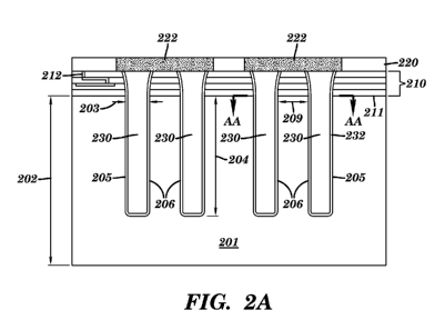
[0013] Figure 2A is a vertical section view of an annular TSV according to the
present
disclosure.
[0014] Figure 2B and 2D are detail views of a TSV according to the present
disclosure.
[0015] Figure 2C is a cross section at AA of a TSV of Figure 2A.
Detailed Description of the Invention
[0016] The present disclosure provides a thermo-mechanically reliable copper
TSV and a
technique to form such TSV during BEOL processing, which is now described in
detail with
accompanying figures. It is noted that like reference numerals refer to like
elements across
different embodiments. The drawings are not necessarily drawn to scale.
[0017] It will be understood that when an element as a layer, region or
substrate is referred to as
being "on" or "over" another element, it can be directly on the other element
or intervening
elements may also be present. In contrast, when an element is referred to as
being "directly on"
or "directly over" another element, there are no intervening elements present.
It will also be
understood that when an element is referred to as being "connected" or
"coupled" to another
element, it can be directly connected or coupled to the other element or
intervening elements
may be present. In contrast, when an element is referred to as being "directly
connected" or
"directly coupled" to another element, there are no intervening elements
present.
[0018] As noted, the present invention identifies a TSV structure and a method
of reliably
forming the same, which structure can withstand CMOS BEOL thermal cycling
without cracking
surrounding materials, thereby providing for a reliable 3D integrated circuit.
CA 02828498 2013-08-23
WO 2012/177585 PCT/US2012/043052
[0019] Referring now to Figure 2A, there is illustrated a semiconductor
substrate 201 having an
initial thickness 202. One or more semiconductor devices (not shown) can be
formed in and on
top surface 211 of the substrate. One or more dielectric layers 210 can be
deposited over top
surface 211. Annular trench 230 can be formed through dielectric layers 210,
extending through
top surface 211 and into substrate 201 utilizing conventional back-end
compatible lithography
and etching. Typically, trench 230 is formed by a Bosch etch which proceeds by
alternating
between anisotropic reactive ion etch and polymer deposition steps, but the
invention is not so
limited. Annular trench 230 does not at this point contact another feature at
its bottom end, so it
can be referred to as a 'blind via'.
[0020] The substrate herein may comprise any semiconductor such as Si, SiGe,
SiGeC, SiC, Ge
alloys, GaAs, InAs, InP and other IIIN or II/VI compound semiconductors. In
addition to these
listed types of semiconducting materials, the present invention also
contemplates cases in which
the semiconductor substrate is a layered semiconductor such as, Si/SiGe,
Si/SiC, silicon-on-
insulators (SOIs) or silicon germanium-on-insulators (SGOIs). Further,
substrate 201 can be
single crystalline, polycrystalline, amorphous, or have a combination of at
least two of a single
crystalline portion, a polycrystalline portion, and an amorphous portion. In a
preferred
embodiment, substrate 201 comprises a single crystalline silicon portion.
[0021] Dielectric layer 210 can include a passivation layer, comprising, e.g.,
5i02, disposed
directly on the semiconductor substrate. Optionally, dielectric layer 210 can
include one or more
additional layers comprising a combination of dielectric and conductive
materials 212, e.g., one
or multiple BEOL interconnect levels of a multilayered interconnect structure,
disposed over the
passivation layer. Dielectric layer 210 can be formed by one or combinations
of any dielectric
material known in the art such as organic insulator (e.g., polyimide),
inorganic insulator (e.g.,
silicon nitride or silicon dioxide), low-K dielectric such as SiLKTM, doped or
undoped silicate
glass, organosilicate, BLOKTM, NBLoKTM, thermosetting polyarylene ethers
(referring to aryl
moieties or inertly substituted aryl moieties which are linked together by
bonds, fused rings, or
inert linking groups such as, for example, oxygen, sulfur, sulfone, sulfoxide,
carbonyl and the
like), or any other type of dielectric material that can be deposited or
formed on a substrate. In
6
CA 02828498 2013-08-23
WO 2012/177585 PCT/US2012/043052
embodiments, the dielectric material has a k-value of 5 or less.
[0022] Referring again to Figure 2A, the length 204 of annular trench 230 is
less than the initial
thickness 202 of substrate 201. Length 204 can be less than 90 microns and
preferably is in the
range of 60 microns or less. At top surface 211, the width 203 of the annular
trench, that is the
separation of inner sidewall 206 and outer sidewall 205, is within the range
of 5 to 10 microns.
Preferably the inner and outer sidewalls of the annular trench at top surface
211 are separated by
a distance within the range of 5.5 to 9 microns.
[0023] The etch process to form annular trench 230 can form nominally straight
sidewalls,
though the sidewalls may actually have a scalloped contour, each 'scallop'
corresponding to a
single etch/polymer deposition cycle of a Bosch process. The height variation
along the sidewall
surface or 'roughness' is preferably minimal, such as between 0 and 0.5
micron. More
particularly, for a given vertical length of a single scallop 'S', the width
of said trench differs by
less than 10 percent, i.e., less than or equal to 0.2*S (accounting for 10
percent variability on
both sidewalls). The sidewalls can be perpendicular to top surface 211 or can
be slightly sloped.
Referring to Figure 2B, sidewalls 205 and 206 can have the same slope relative
to generally
planar top surface 211, but it is not necessary that 205 and 206 have the same
slope. Each
sidewall and the top surface 211 preferably form an angle 208 in the range of
87 to 90 degrees.
According to embodiments of the present invention, sidewalls 205 and 206 angle
toward the
center of the trench such that annular via 230 narrows with depth.
[0024] Figure 2C is a section view at AA of Figure 2A. Annular trench 230
defines an inner
substrate core which can have a circular cross section such that the core
constitutes a generally
cylindrical shape. The diameter 209 of the substrate core at top surface 211
can be in the range
of 4 to 9 microns and preferably is in the range of 5 to 8 microns. The
outside diameter 219 of
annular trench 230 at top surface 211 can be in the range of 18 to 25 microns,
and preferably is
in the range of 19 to 23 microns.
7
CA 02828498 2013-08-23
WO 2012/177585 PCT/US2012/043052
[0025] A magnified view of layer 232 is illustrated in Figure 2D. Layer 232
includes an
insulating liner 233, and can also include several other layers for various
functions such as to
prevent diffusion. Insulating liner 233 can have high conformality and can be
formed, for
example, by sub-atmospheric CVD (SACVD) deposition of Si02 or by deposition of
a flowable
oxide. In certain embodiments, insulating layer 233 is between 0.4 and 1.5
micron thick at the
first (or top) end "T". Insulating liner 233 can be formed on the sidewalls of
the annular trench
230 so that the thickness on sidewalls adjacent to the remote end "R" relative
to the thickness on
sidewalls adjacent to top surface 211 is at least 50 percent or between 65
percent and 100
percent. In embodiments, insulating liner 233 can have a k-value of 5 or less.
[0026] A dielectric cap 234 can be formed to protect insulating liner 233. In
embodiments, an
oxide cap 234 can be formed to fully cover insulating liner 233 within trench
230. Cap layer 234
can be formed by plasma enhanced CVD (PECVD) to a nominal thickness between
1000 and
5000 A measured on the sidewalls adjacent to top surface 211, and thickness at
the remote end at
least 15 percent or in the range of 20 percent to 30 percent of the nominal
thickness.
[0027] Layer 232 can include one or more barrier or adhesion layers 235. A
barrier layer can,
for example, comprise Ta, TaN, Ti, TiN, Ru, RuN, RuTa, RuTaN, W, WN or any
other material
that can serve as a barrier to prevent a conductive material from diffusing
there through. The
actual barrier materials can be selected based on materials of the conductive
TSV core (e.g.,
copper) and the insulating liner 233. In certain embodiments, a barrier 235
can formed by
deposition of Ta/TaN at a thickness between 20 to about 500 A with a thickness
from about 50 to
about 200 A being more typical. The diffusion barrier can be formed by known
methods such as
plasma enhanced CVD (PECVD), ALD, PVD, sputtering, chemical solution
deposition or
plating. For plating, layer 232 will also include a seed layer 236. For a
copper TSV, seed layer
236 can be formed by conventional processes, for example, by PVD or ALD, to a
thickness
within the range of 1000 to 9000 A or in the range of 1500 to 8000 A.
[0028] A void-free fill process, such as available from Novellus or Nexx, can
be used to fill TSV
with copper. The conductive fill may comprise copper or any other conductive
metal, an alloy
8
CA 02828498 2013-08-23
WO 2012/177585 PCT/US2012/043052
comprising at least one conductive metal, a conductive metal silicide or
combinations thereof.
Preferably, the conductive material is a conductive metal such as Cu, W or Al,
with Cu or a Cu
alloy (such as AlCu) being highly preferred in the present invention. The fill
process can be
controlled to result in minimal over burden. Optionally, overburden can be
reduced to about 2
microns or less using a chemical wet etch.
[0029] The structure is then annealed to increase the average grain size to
above 2 microns or to
a size in the range of 3 to 5 microns. The anneal can proceed at temperature
above 300 C. The
structure can be maintained at high temperature for over 15 minutes or in the
range of 20 to 120
minutes. In some embodiments, the structure is maintained in the range of 335
to 410 C for at
least 50 minutes. The structure can be maintained in the range of 350 to 430 C
for 20 to 100
minutes.
[0030] After annealing, the remaining overburden can be removed. Typically,
the overburden
is removed by CMP followed by polishing. Optionally further BEOL layers can be
formed by
conventional BEOL processing over the top end of the TSV. A structure can be
attached to the
top side to enable wafer handling. The backside can be ground or etched to a
thickness of 60 to
90 microns or less so the bottom end of the TSV is exposed, followed as
desired by forming
backside connections to the TSV, including e.g., passivation and contact pads.
[0031] EXAMPLE 1 Annular copper plated TSVs were integrated with minimal
process
complexity to maximize wireability. Blind vias of less than 100 microns depth,
at a minimum
pitch of 50 microns, with near vertical sidewalls, were made by Bosch process.
A deposited
conformal oxide, with excellent coverage at the bottom of the TSV, was used
for insulation.
Sputter deposition was used for a barrier and seed layer, then bottom-up void-
free copper plating,
anneal and CMP to remove the minimal plated overburden. A thick Cu wiring
level takes
advantage of the lower voltage drops observed with TSV's but results in
additional bowing. A
process that incorporates a highly compressive ILD film was used at key via
levels to
compensate for the increased bow. Completed wafers were bonded to glass
handlers and thinned
by grind, polish, RIE. PECVD oxide/nitride was deposited. After CMP to expose
the TSV
9
CA 02828498 2013-08-23
WO 2012/177585 PCT/US2012/043052
metal, copper was electrodeposited and a backside redistribution level was
defined. The wafers
were diced and assembled on organic laminates using die level C4 joining.
Reliability testing
was performed. A thin (<1000A) SiN cap (top side) layer remained intact after
a 399 C soak.
Tests for ILD damage found no change in the leakage between wiring levels
after thermal
cycling between -65C and 150 C for 500 cycles. Thermal cycling also showed no
degradation
in TSV resistance or functionality of devices proximate to the TSV.
[0032] While the present invention has been particularly shown and described
with respect to
preferred embodiments thereof, it will be understood by those skilled in the
art that the foregoing
and other changes in forms and details may be made without departing from the
spirit and scope
of the present invention. It is therefore intended that the present invention
not be limited to the
exact forms and details described and illustrated, but fall within the scope
of the appended
claims.