Note: Descriptions are shown in the official language in which they were submitted.
CA 02829433 2013-10-04
46159-CA-PAT
MOBILE WIRELESS COMMUNICATIONS DEVICE WITH MULTIPLE-BAND ANTENNA
AND RELATED METHODS
Technical Field
[0001] The present invention relates to the field of
communications, and, more particularly, to wireless
communications and related methods.
Background
[0002] Cellular communication systems continue to grow in
popularity and have become an integral part of both personal and
business communications. Cellular telephones allow users to
place and receive phone calls almost anywhere they travel.
Moreover, as cellular telephone technology is improved, so too
has the functionality of cellular devices. For example, many
cellular devices now incorporate Personal Digital Assistant
(PDA) features such as calendars, address books, task lists,
calculators, memo and writing programs, etc. These multi-
function devices usually allow users to wirelessly send and
receive electronic mail (email) messages and access the Internet
via a cellular network and/or a wireless local area network
(TAMAN), for example.
[0003] As the functionality of cellular devices continues to
increase, so too does demand for smaller devices that are easier
and more convenient for users to carry. Nevertheless, the move
towards multi-functional devices makes miniaturization more
difficult as the requisite number of installed components
increases. Indeed, the typical cellular device may include
several antennas, for example, a cellular antenna, a global
positioning system antenna, and a WiFi IEEE 802.11g antenna.
These antennas may comprise external antennas and internal
antennas.
1
CA 02829433 2013-10-04
46159-CA-PAT
[0004] Generally speaking, internal antennas allow cellular
devices to have a smaller footprint. Moreover, they are also
preferred over external antennas for mechanical and ergonomic
reasons. Internal antennas are also protected by the cellular
device's housing and therefore tend to be more durable than
external antennas. External antennas may be cumbersome and may
make the cellular device difficult to use, particularly in
limited-space environments. Yet, one potential drawback of
typical internal antennas is that they are in relatively close
proximity to the user's head when the cellular device is in use,
thereby increasing the specific absorption rate (SAR). Yet
more, hearing aid compatibility (HAC) may also be affected
negatively. Also, other components within the cellular device
may cause interference with or may be interfered by the internal
antenna.
Brief Description of the Drawings
[0005] FIG. 1 is a schematic diagram of an example embodiment
of the mobile wireless communications device.
[0006] FIG. 2 is a top plan view of an example embodiment of
a multiple-band antenna from the mobile wireless communications
device of FIG. 1.
[0007] FIG. 3 is a side elevation view of the multiple-band
antenna of FIG. 2.
[0008] FIG. 4 is a top plan view of another example
embodiment of a multiple-band antenna from the mobile wireless
communications device of FIG. 1.
[0009] FIG. 5 is a side elevation view of the multiple-band
antenna of FIG. 4.
[0010] FIG. 6 is a top plan view of yet another example
embodiment of a multiple-band antenna from the mobile wireless
communications device of FIG. 1 with the dielectric substrate
2
CA 02829433 2013-10-04
46159-CA-PAT
removed.
[0011] FIG. 7 is a side elevation view of the multiple-band
antenna of FIG. 6.
[0012] FIG. 8 is a current distribution diagram of an example
embodiment of a secondary radiator in an antenna that excites
mode 3.
[0013] FIG. 9A is a current distribution diagram of an
example embodiment of a primary radiator in the mobile wireless
communications device in a first mode.
[0014] FIGS. 9B-9D are far field patterns of an example
embodiment of a primary radiator in the mobile wireless
communications device in a first mode.
[0015] FIG. 10A is a current distribution diagram of an
example embodiment of a primary radiator in the mobile wireless
communications device in a second mode.
[0016] FIGS. 10B-10D are far field patterns of an example
embodiment of a primary radiator in the mobile wireless
communications device in a second mode.
[0017] FIG. 11A is a current distribution diagram of an
example embodiment of a primary radiator in the mobile wireless
communications device in a third mode.
[0018] FIGS. 11B-11D are far field patterns of an example
embodiment of a secondary radiator in the mobile wireless
communications device in a third mode.
[0019] FIG. 12 is a schematic block diagram illustrating
example components of a mobile wireless communications device
that may be used with the mobile wireless communications device
of FIG. 1.
Detailed Description of the Preferred Embodiments
[0020] The present description is made with reference to the
accompanying drawings, in which embodiments are shown. However,
3
CA 02829433 2013-10-04
46159-CA-PAT
many different embodiments may be used, and thus the description
should not be construed as limited to the embodiments set forth
herein. Rather, these embodiments are provided so that this
disclosure will be thorough and complete. Like numbers refer to
like elements throughout, and prime notation is used to indicate
similar elements in alternative embodiments.
[0021] Generally speaking, a mobile wireless communications
device may include a housing, at least one wireless transceiver
carried by the housing and having a primary output, and a
secondary output, and a multiple-band antenna carried by the
housing and coupled to the at least one wireless transceiver.
The multiple-band antenna may include a dielectric substrate and
a pattern of electrically conductive traces thereon defining a
primary radiator and a secondary radiator spaced apart from the
primary radiator. The primary radiator may include a first
elongate member having a primary feed coupled to the primary
output, and a first reference member spaced from the first
elongate member and at least partially laterally surrounding the
first elongate member and coupled to a reference voltage. The
secondary radiator may include a second elongate member having a
secondary feed coupled to the secondary output.
[0022] More specifically, the first reference member may
comprise a first arm, and a second arm coupled thereto. The
first arm may have an L-shape, and the second arm may comprise a
proximal portion coupled to the first arm and having an L-shape,
and a distal portion extending away from the proximal portion.
[0023] Additionally, the first arm may extend along a bottom
of the housing. The second elongate member may have a first
arm, and a second arm coupled thereto. The secondary feed may
be on the second arm, and the first arm may extend at least
partially along a bottom edge of the housing. The dielectric
substrate may have a non-planar shape. The dielectric substrate
4
ak 02829433 2013-10-04
46159-CA-PAT
may be carried by a bottom of the housing, and the primary and
secondary radiators may be carried by respective opposing first
and second sides of the dielectric substrate. For example, the
at least one wireless transceiver may comprise a Long Term
Evolution (LTE) transceiver configured to operate the primary
and secondary outputs in an LTE carrier aggregation mode.
[0024] Another aspect is directed to a method of making a
multiple-band antenna for a mobile wireless communications. The
method may comprise forming a multiple-band antenna to comprise
a dielectric substrate and a pattern of electrically conductive
traces thereon defining a primary radiator and a secondary
radiator spaced apart from the primary radiator. The primary
radiator may comprise a first elongate member having a primary
feed coupled to the primary output, and a first reference member
spaced from the first elongate member and at least partially
laterally surrounding the first elongate member and coupled to a
reference voltage. The secondary radiator may comprise a second
elongate member having a secondary feed coupled to the secondary
output.
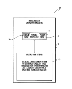
[0025] Referring initially to FIGS. 1-3, a mobile wireless
communications device 20 according to the present disclosure is
now described. The mobile wireless communications device 20
illustratively includes a housing 22, a wireless transceiver 21
carried by the housing and having a primary and secondary
outputs 55, 56, and a multiple-band antenna 23 carried by the
housing and coupled to the wireless transceiver. For example,
the wireless transceiver 21 may comprise an LTE transceiver
configured to operate the primary and secondary outputs 55, 56
in an LTE carrier aggregation mode. In the illustrated
embodiment, the multi-band antenna 23 may operate the primary
output 55 at: LTE Band 7, 3, 8, 20, Primary; Wideband Code
Division Multiple Access (WCDMA) Band 1, 2, 5, 8, Primary;
CA 02829433 2013-10-04
46159-CA-PAT
Global System for Mobile Communications (GSM) 850, 900, 1800,
1900; and operate the secondary output 56 at LTE Band 7, 3, 8,
20, Multiple Input Multiple Output (MIM0); WCDMA Band 1, 2, 5, 8
Diversity.
[0026] The multiple-band antenna 23 illustratively includes a
dielectric substrate 24 and a pattern of electrically conductive
traces thereon defining a primary radiator 26 and a secondary
radiator 25 spaced apart from the primary radiator. The
dielectric substrate 24 illustratively includes a non-planar
shape, which illustratively fits the interior portions of the
housing 22. The dielectric substrate 24 may be carried by a
bottom of the housing 22, and the primary and secondary
radiators 26, 25 may be carried by respective opposing first and
second sides of the dielectric substrate.
[0027] The primary radiator 26 illustratively includes a
first elongate member 32 having a primary feed 27 coupled to the
primary output 55. The primary radiator 26 illustratively
includes a first reference member 33 (e.g. ground reference
member) spaced from the first elongate member 32 and at least
partially laterally surrounding the first elongate member and
coupled to a reference voltage (e.g. ground). The secondary
radiator 25 illustratively includes a second elongate member
having a secondary feed 31 coupled to the secondary output 56.
More specifically, the first reference member 33 illustratively
includes a first arm 35, and a second arm 51 coupled thereto.
[0028] In detail, the first elongate member 32 has a
substantially rectangular-shape, and extends in parallel with
the first arm 35 of the first reference member 33 (bending
upward slightly). The first elongate member 32 illustratively
includes a top portion defining a recess 57, and a protruding
portion 58 partially extending across the recess and including
the primary feed 27.
6
CA 02829433 2013-10-04
46159-CA-PAT
[0029] The first arm 35 of the first reference member 33 is
substantially rectangle-shaped, and illustratively includes a
proximal portion 59, and a distal portion 60 coupled thereto and
having an enlarged width. The distal portion 60 also defines a
notch 61 having parallel sides, and a curved end. Additionally,
the first arm 35 extends along a bottom of the housing 22.
[0030] The second arm 51 comprises a proximal portion 41
coupled to the first arm 35 and having an L-shape, and a distal
portion 42 extending away from the proximal portion and having a
rectangular-shape. The distal portion 42 illustratively
includes a reference connection 28 (e.g. ground connection), and
defines a recess 62 having a curved end. The proximal and
distal portions 41, 42 have straight sides.
[0031] The first reference member 33 illustratively includes
a third arm 47 extending almost entirely across the bottom edge
of the dielectric substrate 24. The third arm 47 illustratively
includes a proximal portion 62, and a distal portion 63 coupled
thereto. The proximal portion 62 is rectangle-shaped, and the
distal portion 63 is also rectangle-shaped. The distal portion
63 illustratively includes a greater width than that of the
proximal portion 62 and has a rectangle-shaped notch 64 adjacent
a corner thereof. The distal portion 63 also illustratively
defines a square-shaped opening 65.
[0032] The second elongate member illustratively includes a
first arm 46, and a second arm 34 coupled thereto. The
secondary feed 31 illustratively is on the second arm 34, and
the first arm 46 may extend at least partially along a bottom
edge of the housing 22. In particular, the first arm 46
illustratively includes rectangle-shaped proximal and distal
portions 66, 67, the distal portion defining a rectangle-shaped
recess 68 on a side thereof. The second arm 34 illustratively
includes a proximal portion 110, a medial portion 111 coupled to
7
CA 02829433 2013-10-04
46159-CA-PAT
the proximal portion, and a distal portion 112 coupled to the
medial portion. The proximal portion 110 is rectangle-shaped,
and the medial portion 111 is U-shaped. The distal portion 112
comprises an L-shaped portion coupled to the medial portion 111,
and a rectangle-shaped portion coupled to the L-shaped portion.
[0033] Another aspect is directed to a method of making a
multiple-band antenna 23 for a mobile wireless communications
20. The method may comprise forming a multiple-band antenna 23
to comprise a dielectric substrate 24 and a pattern of
electrically conductive traces thereon defining a primary
radiator 26 and a secondary radiator 25 spaced apart from the
primary radiator. The primary radiator 26 may comprise a first
elongate member having a primary feed 27 coupled to the primary
output, and a first reference member 33 spaced from the first
elongate member and at least partially laterally surrounding the
first elongate member and coupled to a reference voltage. The
secondary radiator 25 may comprise a second elongate member
having a secondary feed 31 coupled to the secondary output.
[0034] Referring now additionally to FIGS. 4-5, another
embodiment of the multiple-band antenna 23' is now described.
In this embodiment of the multiple-band antenna 23', those
elements already discussed above with respect to FIGS. 1-3 are
given prime notation and most require no further discussion
herein. This embodiment differs from the previous embodiment in
that the first arm 35' illustratively has an L-shape, and
uniform width throughout. The first arm 35' also does not
include the recess from the embodiments of FIGS. 2-3. The third
arm 47' also does not include the notch of the prior embodiment,
but does include an L-shaped turn 120' in a medial portion
thereof. The second arm 34' of the secondary radiator 25'
illustratively includes a single L-shaped turn 121', rather the
multiple turns of the prior embodiments. In the illustrated
8
CA 02829433 2013-10-04
46159-CA-PAT
embodiment, the multi-band antenna 23' may operate the primary
output 55' at: LTE Band 4, 13 Primary; CDMA lx Voice, EVDO
Diversity; WCDMA Band 1, 2, 5, 8 Primary; GSM 850, 900, 1800,
1900; and operate the secondary output 56' at: LTE Band 13 MIMO;
CDMA lx Voice Primary; and CDMA lx EVDO Diversity.
[0035] Referring now additionally to FIGS. 6-7, another
embodiment of the multiple-band antenna 23" is now described.
In this embodiment of the multiple-band antenna 23", those
elements already discussed above with respect to FIGS. 1-3 are
given double prime notation and most require no further
discussion herein. This embodiment differs from the previous
embodiment in that the third arm 47" includes the rectangle-
shaped recess 64" in a medial portion rather than the corner of
the embodiment of FIGS. 2-3. Also, the secondary radiator 25"
has a general C-shape including the first and second arms 46",
34". The first arm 46" illustratively includes a pair of
rectangle-shaped branches 115', 116'. The second arm 34"
illustratively has an L-shape and is rectangle-shaped
throughout. In the illustrated embodiment, the multi-band
antenna 23" may operate the primary output 55" at: LTE Band 2,
4, 5, 17 Primary; WCDMA Band 1, 2, 5, 8 Primary; GSM 850, 900,
1800, 1900; and operate the secondary output 56" at: LTE Band
2, 4, 5, 17 MIMO; WCDMA Band 1, 2, 5, 8 Diversity.
[0036] With regards to the operating bands of the embodiments
of FIGS. 2-7, the operating frequencies are shown in Table 1
herein.
9
CA 02829433 2013-10-04
46159-CA-PAT
Band,;,,4= FrequencyRange(Nniz)
LTE17 704-746
LTE13 746-777
LTE20 791-862
LTEMNCDMA5 824-894
GSM 850
COMA1xCell
LTEAMCDMA8 880-960
GSM 900
LTE3 1710-1880
LTE1NCDMA4Tx
GSM 1800
LTEMNCDMA2 1850-1990
GSM1900
COMA1xPCS
MDMA1 1920-2170
LTE7 2500-2690
Table 1: Operating Frequencies
[0037] Theory of Operation
The basis of this multiple-band antenna 23 relies on exciting
different characteristics modes in the chassis of the mobile
wireless communications device 20. Characteristics modes
describe the current distribution and far field radiation that
are unique to a given conducting body at a specific frequency.
In theory, a metallic object could possess infinite number of
characteristic mode for a given frequency, however not all modes
are excitable in practice. Mathematically, characteristics
modes on a metal object are precisely described by the following
close boundary problem:
[LW ¨ = 0 .
where the operator L is defined as
L(/) 'icoAGO VcIV); and
A and 41 are the vector and scalar potentials due to a given
current distribution respectively.
CA 02829433 2013-10-04
46159-CA-PAT
[0038] Since A and 43 are integrals defined over the closed
surface, the problem can be rewritten in terms of impedances and
arrive at the eigenvalues problem as
= LW.; and
Z(J) = 01W;
where matrix M is a symmetric matrix that diagonalizes the
matrix Z, vare the eigenvalues, and J are the eigenvectors. A
characteristic mode refers to a given set of eigenvalue and
eigenvector.
[0039] By definition, the eigenvectors associated with a
particular conducting body are orthogonal to each other and must
satisfy the orthogonality relationships OrmIZI-n)= ,f rni*n
In other words, the current distribution and radiation pattern
of one mode is un-correlated to the current distribution and
radiation pattern of another mode, even though there is only one
radiating element. By exploiting this orthogonality principle
of characteristic modes, the multiple-band antenna 23 can
achieve low correlation at low frequencies despite having only
one radiator and it is this particular property that enables
this feature. More specifically, the first elongate member 32
in N-series excites a dominant mode 1 (vvA) and the secondary
radiator 25 excites a dominant mode 3 (v:PLO.
[0040] Referring now to FIGS. 8-11D, diagram 77 shows the
current distribution, and diagrams 79, 81, 83 show the far field
patterns for the mobile wireless communications device 20 while
in mode 1 at 704 MHz. Diagram 85 shows the current
distribution, and diagrams 87, 89, 91 show the far field
patterns for the mobile wireless communications device 20 while
in mode 2 at 704 MHz. Diagrams 93, 70 show the current
11
CA 02829433 2013-10-04
46159-CA-PAT
distribution, and diagrams 95, 97, 99 show the far field
patterns for the mobile wireless communications device 20 while
in mode 3 at 704 MHz.
[0041] The multiple-band antenna 23 may exploit the natural
resonances, known as characteristics modes, of an arbitrary
metallic object to achieve low correlation between multiple
antennas in a MIMO system. Typical MIMO systems may rely on an
antenna array where the antenna elements are usually separated
from each other by half of a wavelength. For low frequency LTE
bands, such as Band 17 (704 MHz - 746 MHz) or Band 13 (746 MHz -
777 MHz), the half wavelength spatial separation may not be
achievable in handheld devices, such as a smartphone where the
overall dimension of the device is on the order of a quarter
wavelength of the operating wavelength. Low frequency is
particularly interesting because radiation at low frequencies is
predominantly due to the mobile device's chassis and the antenna
element serves as an excitation element. Consequently, the
current distributions excited by each antenna element in a MIMO
system share one radiator, i.e. the chassis of the device. This
is in conflict to the multi-antenna requirement of MIMO because
multiple antennas usually mean that there are multiple radiating
elements, which may not be true in a handset. The multiple-band
antenna 23 may relax this requirement and enable: high
performance MIMO with a single radiating element; and systematic
antenna element placement with minimal correlation and gain
imbalance.
[0042] With regards to Table 2 below, the measured
performance of the multi-band antenna 23 in varying operating
frequencies is shown. Of particular interest is the LTE MIMO
and Correlation section, which demonstrate the low correlation
values achieved with the multi-band antenna 23.
12
CA 0 2 8 2 9 4 3 3 2 0 13 - 10 - 0 4
46159 -CA -PAT
verkon
LTE 9884810MHz BW
Conducted Required Conducted
Voice Power TRP Gain Meanued Gain Sensitivity
715 Regired fel Meastued Gain
Gel (F5) 24 -fa 4=44 41 -5A -108 401 4.4 43
Malin 1.4 1.0 16 Fitargitt 1.6 1 0 11
PCS (15) 34 19 . -5 -11 -4.8 -49 -107 -101 --6 -
52 -5,7 -6.0
liUrgin -0.1 05 05 WW1 C. 1' 03 0
Conducted Required CaKluct e-d
EVDO Power TRP Gain Meastued Gain Seas.icarly 75
Ranked Gain Measured Gain
CeCTS) 2Y74 la -6 46 -51) -5.0 itt.õ. -109.5
ARS -7 -5A -53 -12
Margin IA 5.0 01 Margin 16 1 1.S
PES 151 - 24 - 19 - -5 4.1 41 -- *--- 408 5 -
402.5 4 41 :4 -60
- Margin -0_1 c Margin
Conducted Required Conducted
LIE Power TRP Gait Measured Gain Sensitivity T5
Required Gain Measured Gain
Rand13 215 55 -5.2 -5.0 4.5 445 41 -75 -6.6
-63 -St
Margin 0.3 05 0.0 Mwgin 09 12 09
Rand 4 = 235. 19 -45 -43 -3.8 -32,Ti; -97 _ -91 -
4 4.1 i4.7
Margin 92 '1 7 1 7 Ma* D
mnductW
LTE Sensitivity its Required Gain
Measured Gain Delta with Primly
Rand 13 -983 48 40.7 -95 4.7 -
93- 31 3.4 16
Margin 0.9 1.0 1,4
Vind 4 -
-97 48 40 -17.t -7.9 -73
4J 31 16
- -
Ma rtn ao 51 17
Correlation Rewired Measured
Died 13 03 033 032 0.3t
Margin 037 110 0 11
Sande0.5 0.060070.01
Margn 44 ;
UWWA
amay Sensitivity TIS Winked Gait
Measured Gain Deka wftb Prinary
Cell (I'S) -1011 45 43 -92 -9.3 -
93 31 4.1 4,0
Margin P 3- 17
PCS n 407 -95 U 33 -39 M-7.-
1 5 1.9 2.4
- 1= won s 8 15
Table 2: Measured Performance
[0043] Example components of a mobile wireless communications
device 1000 that may be used in accordance with the above-
described embodiments are further described below with reference
to FIG. 12. The device 1000 illustratively includes a housing
1200, a keyboard or keypad 1400 and an output device 1600. The
output device shown is a display 1600, which may comprise a full
graphic liquid crystal display (LCD). Other types of output
devices may alternatively be utilized. A processing device 1800
is contained within the housing 1200 and is coupled between the
13
CA 02829433 2013-10-04
46159-CA-PAT
keypad 1400 and the display 1600. The processing device 1800
controls the operation of the display 1600, as well as the
overall operation of the mobile device 1000, in response to
actuation of keys on the keypad 1400.
[0044] The housing 1200 may be elongated vertically, or may
take on other sizes and shapes (including clamshell housing
structures). The keypad may include a mode selection key, or
other hardware or software for switching between text entry and
telephony entry.
[0045] In addition to the processing device. 1800, other parts
of the mobile device 1000 are shown schematically in FIG. 12.
These include a communications subsystem 1001; a short-range
communications subsystem 1020; the keypad 1400 and the display
1600, along with other input/output devices 1060, 1080, 1100 and
1120; as well as memory devices 1160, 1180 and various other
device subsystems 1201. The mobile device 1000 may comprise a
two-way RF communications device having data and, optionally,
voice communications capabilities. In addition, the mobile
device 1000 may have the capability to communicate with other
computer systems via the Internet.
[0046] Operating system software executed by the processing
device 1800 is stored in a persistent store, such as the flash
memory 1160, but may be stored in other types of memory devices,
such as a read only memory (ROM) or similar storage element. In
addition, system software, specific device applications, or
parts thereof, may be temporarily loaded into a volatile store,
such as the random access memory (RAM) 1180. Communications
signals received by the mobile device may also be stored in the
RAM 1180.
[0047] The processing device 1800, in addition to its
operating system functions, enables execution of software
applications 1300A-1300N on the device 1000. A predetermined
14
ak 02829433 2013-10-04
46159-CA-PAT
set of applications that control basic device operations, such
as data and voice communications 1300A and 1300B, may be
installed on the device 1000 during manufacture. In addition, a
personal information manager (PIN) application may be installed
during manufacture. The PIN may be capable of organizing and
managing data items, such as e-mail, calendar events, voice
mails, appointments, and task items. The PIN application may
also be capable of sending and receiving data items via a
wireless network 1401. The PIN data items may be seamlessly
integrated, synchronized and updated via the wireless network
1401 with corresponding data items stored or associated with a
host computer system.
[0048] Communication functions, including data and voice
communications, are performed through the communications
subsystem 1001, and possibly through the short-range
communications subsystem 1020. The communications subsystem
1001 includes a receiver 1500, a transmitter 1520, and one or
more antennas 1540 and 1560. In addition, the communications
subsystem 1001 also includes a processing module, such as a
digital signal processor (DSP) 1580, and local oscillators (L0s)
1601. The specific design and implementation of the
communications subsystem 1001 is dependent upon the
communications network in which the mobile device 1000 is
intended to operate. For example, a mobile device 1000 may
include a communications subsystem 1001 designed to operate with
the NobitexTM, Data TACm or General Packet Radio Service (GPRS)
mobile data communications networks, and also designed to
operate with any of a variety of voice communications networks,
such as Advanced Mobile Phone System (AMPS), time division
multiple access (TDMA), code division multiple access (CDMA),
Wideband code division multiple access (W-CDMA), personal
communications service (PCS), GSM (Global System for Mobile
CA 02829433 2013-10-04
46159-CA-PAT
Communications), enhanced data rates for GSM evolution (EDGE),
etc. Other types of data and voice networks, both separate and
integrated, may also be utilized with the mobile device 1000.
The mobile device 1000 may also be compliant with other
communications standards such as 3GSM, 3rd Generation
Partnership Project (3GPP), Universal Mobile Telecommunications
System (UMTS), 4G, etc.
[0049] Network access requirements vary depending upon the
type of communication system. For example, in the Mobitex and
DataTAC networks, mobile devices are registered on the network
using a unique personal identification number or PIN associated
with each device. In GPRS networks, however, network access is
associated with a subscriber or user of a device. A GPRS device
therefore typically involves use of a subscriber identity
module, commonly referred to as a SIN card, in order to operate
on a GPRS network.
[0050] When required network registration or activation
procedures have been completed, the mobile device 1000 may send
and receive communications signals over the communication
network 1401. Signals received from the communications network
1401 by the antenna 1540 are routed to the receiver 1500, which
provides for signal amplification, frequency down conversion,
filtering, channel selection, etc., and may also provide analog
to digital conversion. Analog-to-digital conversion of the
received signal allows the DSP 1580 to perform more complex
communications functions, such as demodulation and decoding. In
a similar manner, signals to be transmitted to the network 1401
are processed (e.g. modulated and encoded) by the DSP 1580 and
are then provided to the transmitter 1520 for digital to analog
conversion, frequency up conversion, filtering, amplification
and transmission to the communication network 1401 (or networks)
via the antenna 1560.
16
ak 02829433 2013-10-04
46159-CA-PAT
[0051] In addition to processing communications signals, the
DSP 1580 provides for control of the receiver 1500 and the
transmitter 1520. For example, gains applied to communications
signals in the receiver 1500 and transmitter 1520 may be
adaptively controlled through automatic gain control algorithms
implemented in the DSP 1580.
[0052] In a data communications mode, a received signal, such
as a text message or web page download, is processed by the
communications subsystem 1001 and is input to the processing
device 1800. The received signal is then further processed by
the processing device 1800 for an output to the display 1600, or
alternatively to some other auxiliary I/O device 1060. A device
may also be used to compose data items, such as e-mail messages,
using the keypad 1400 and/or some other auxiliary I/O device
1060, such as a touchpad, a rocker switch, a thumb-wheel, or
some other type of input device. The composed data items may
then be transmitted over the communications network 1401 via the
communications subsystem 1001.
[0053] In a voice communications mode, overall operation of
the device is substantially similar to the data communications
mode, except that received signals are output to a speaker 1100,
and signals for transmission are generated by a microphone 1120.
Alternative voice or audio I/O subsystems, such as a voice
message recording subsystem, may also be implemented on the
device 1000. In addition, the display 1600 may also be utilized
in voice communications mode, for example to display the
identity of a calling party, the duration of a voice call, or
other voice call related information.
[0054] The short-range communications subsystem enables
communication between the mobile device 1000 and other proximate
systems or devices, which need not necessarily be similar
devices. For example, the short-range communications subsystem
17
CA 02829433 2013-1()-04
46159-CA-PAT
may include an infrared device and associated circuits and
components, a BluetoothTM communications module to provide for
communication with similarly-enabled systems and devices, or a
NFC sensor for communicating with a NFC device or NFC tag via
NFC communications.
[0055] Many modifications and other embodiments will come to
the mind of one skilled in the art having the benefit of the
teachings presented in the foregoing descriptions and the
associated drawings. Therefore, it is understood that various
modifications and embodiments are intended to be included within
the scope of the appended claims.
18