Note: Descriptions are shown in the official language in which they were submitted.
CA 02829445 2013-10-04
ELECTROOPTIC DEVICE
TECHNICAL FIELD
[0001]
The present invention relates to an electrooptic device,
and more particularly relates to an electrooptic device that
changes the refractive index of an electrooptic crystal by
controlling the electric field of the crystal, so that the
forwarding direction of light can be changed, or the phase
of light can be changed.
BACKGROUND ART
[0002]
At present, requests for an optical control device that
deflects a laser beam have increased for video apparatuses,
such as projectors, laser printers, confocal microscopes having
a high resolution, barcode readers, etc. As optical deflection
techniques, a technique for rotating a polygon mirror, a
technique for employing a galvano mirror to control the deflected
direction of light, a diffraction technique that employs the
acousto-optic effect, and a micro machine technique called
the MEMS (Micro Electro Mechanical System) have been proposed.
[0003]
As for a polygon mirror, a mirror having the shape of
a polyhedron is mechanically rotated, and the reflection
direction of a laser beam is sequentially changed to deflect
- 1 -
CA 02829445 2013-10-04
light. Since a method employing a polygon mirror utilizes
mechanical rotations, the rotational speed is limited. That
is, the acquisition of revolutions equal to or greater than
10000 rpm is difficult for a polygon mirror, and there is a
fault in that a polygon mirror is not appropriate for an
application required for a rapid operation. A method employing
a polygon mirror has been utilized for the deflection of the
laser beam of a laser printer. However, the limit imposed
by the rotational speed of a polygon mirror is a bottleneck
when it comes to increasing the printing speed of a printer.
In order to further increase the printing speed of a printer,
a faster optical deflection technique is required.
[0004]
A galvano mirror is employed for a laser scanner, etc.,
that deflects and scans a laser beam. A conventional practical
galvano mirror has, for example, a magnetic path formed by
a moving iron core, which is used instead of a moving coil
arranged in a magnetic field, and a magnetic member, around
which two permanent magnets and four magnetic poles are arranged.
When the magnetic fluxes between the magnetic poles are changed
by the magnitude and the direction of a current that flows
across a drive coil that is wound around the magnetic member,
a reflecting mirror is moved via the moving iron core and the
laser beam is deflected and scanned. The method employing
a galvano mirror can perform a rapid operation. However, since
the drive coil of a conventional galvano mirror is provided
by a machine winding, downsizing is difficult. Therefore,
- 2 -
CA 02829445 2013-10-04
it is difficult for the sizes of a laser scanning system employing
a galvano mirror and a laser application apparatus that employs
this system to be further reduced. Furthermore, there is a
fault that power consumption is large. There is another fault
in that a rapid operation can not be performed within a cycle
of the MHz unit.
[0005]
An optical deflector of an optical diffraction type that
employs the acousto-optic effect has been put to practical
use. However, a method employing this optical deflector of
an optical diffraction type consumes a large amount of power
and downsizing is difficult. Further, there is a fault in
that it is difficult to obtain a large deflection angle and
to perform a rapid operation. In addition, since a method
employing the MEMS electrostatically drives a fine mirror as
an optical deflection device, several tens of p.m is the limit
placed on the response.
[0006]
Conventionally, various optical function parts employing
an electrooptic crystal have been put to practical use. These
optical function parts employ a phenomenon such that, upon
the application of a voltage to an electrooptic crystal, the
refractive index of the crystal is changed by the electrooptic
effect. Thus, as means for solving the above described problems ,
a technique has been developed whereby a voltage is applied
to the electrodes of an electrooptic crystal, and a beam is
deflected by the electrooptic effect (see, for example, patent
- 3 -
CA 02829445 2013-10-04
document 1) . Furthermore, a technique has been developed
whereby a beam is deflected using an electrooptic crystal that
is processed in a prism shape, or an electrooptic crystal wherein
electrodes having a prism shape are formed (see, for example,
patent document 2) . When a voltage is applied to the electrodes
of the electrooptic crystal, the refractive index can be changed
because of the electrooptic effect. By using the method that
employs electrodes shaped like a prism, an area where the
refractive index is changed and an area where a voltage is
not applied, and a refractive index is not changed, are produced
in the electrooptic crystal. Due to a refractive index
difference at the boundary of the two areas, a beam is deflected,
and a deflection angle is obtained.
[0007]
By using the method employing the electrooptic crystal,
a response up to the speed limit of the electrooptic effect
is available, and a response exceeding one GHz can be obtained.
In the past, reports of using LiNb03 (hereinafter referred
to as an LN crystal) and PLZT were submitted as optical deflection
devices employing an electrooptic crystal. However, since
a device employing the LN crystal produces only a small
electrooptic effect, there is a fault in that only a deflection
angle of about 3 mrad is obtained by applying a voltage of
about 5 kV/mm. Further, also for a device using PLZT, a
deflection angle of about 45 mrad is the limit, relative to
the application of an electric field of 20 kV/mm (see, for
example, non-patent document 1) .
- 4 -
CA 02829445 2013-10-04
[0008]
However, according to the conventional method, there is
only a small change of the refractive index in each prism area
due to the electrooptic effect, and the deflection angle due
to the refractive index change is also small. Therefore, in
order to obtain a large deflection angle, a plurality of prisms
must be arranged for the conventional method. However, in
a case wherein a plurality of prisms are arranged, there is
a problem in that, when light enters the prisms at a large
incident angle, a desired resolution can not be obtained.
[0009]
On the other hand, an optical phase modulator employing
an electrooptic crystal changes the refractive index of the
crystal to change the speed at which light passes through the
crystal, and to change the phase of the light. Further, when
the electrooptic crystal is located on one of the optical
waveguide paths of a Mach-Zehnder interferometer and a Michelson
interferometer, the light intensity of the output of the
interferometer is changed in accordance with a voltage applied
to the crystal. These interferometers can be employed as optical
switches or optical modulators.
[0010]
Fig. 1 shows the structure of a conventional optical phase
modulator employing an electrooptic crystal. In the optical
phase modulator, a positive electrode 2 and a negative electrode
3 are formed on opposite faces of the block of an electrooptic
crystal 1. The crystal axes x, y and z of the electrooptic
- 5 -
CA 02829445 2013-10-04
crystal 1 are defined as shown in Fig. 1. The change in the
refractive index due to the electrooptic effect is provided
by the linear Pockels effect and the quadratic Kerr effect.
In the case of the quadratic Kerr effect, sll is an electrooptic
constant for vertically polarized light, i.e., for the
polarization direction relative to the x axial direction in
Fig. 1. The change in a phase when a voltage V is applied
between the positive electrode 2 and the negative electrode
3 is provided by the following expression.
[0011]
[Expression 11
0
=
rcn3Lsn(v)2 (1)
d)
Here, n denotes the refractive index of the electrooptic
crystal 1, L denotes a light propagation direction, i.e., the
length of the electrooptic crystal 1 in the z axial direction
in Fig. 1, X denotes the wavelength of light, and d denotes
the interval between the positive electrode 2 and the negative
electrode 3. s12 is an electrooptic constant for horizontally
polarized light, i.e., for a polarization direction relative
to the y axial direction in Fig. 1, and the change in a phase
when a voltage V is applied between the positive electrode
2 and the negative electrode 3 is obtained by using the following
expression.
[0012]
[Expression 2]
- 6 -
=
CA 02829445 2013-10-04
an 3 LS/ 2 V
Oy _________________ (2)
A half-wave voltage is employed as an index that represents
the efficiency of the optical phase modulator. A half-wave
voltage is a voltage that is required to change the phase of
light by TC radian, and is provided by the following expression.
[0013]
[Expression 3]
v7rAd 2
= 3 ______________ (3)
n Ls u
Next, an explanation will be given for a light intensity
modulator that is constituted by combining an optical phase
modulator, a polarizer and an analyzer. Figs. 2A and 2B show
the structure of a conventional light intensity modulator.
As shown in Fig. 2A, a positive electrode 2 and a negative
electrode 3 are formed on opposite faces of an electrooptic
crystal 1. A polarizer 4 is located on the incidence side
of the electrooptic crystal 1, and an analyzer 5 is located
on the emittance side. Of the field elements of light that
is passed through the polarizer 4, the element parallel to
the x axis is defined as Ex, and the element parallel to the
y axis is defined as Ey. In a case wherein the polarization
angle of the polarizer 4 is 45 degrees relative to the x axis
of the electrooptic crystal 1, Ex = Ey.
[0014]
The changes in the phases of Ex and Ey upon the application
of a voltage V between the positive electrode 2 and the negative
- 7 -
CA 02829445 2013-10-04
electrode 3 are respectively obtained by expressions (1) and
(2). In a case wherein the polarization angle of the analyzer
is 45 degrees relative to the x axis of the electrooptic
crystal 1, the intensity of the output light that is passed
through the analyzer 5 is provided by the following expression.
[0015]
[Expression 4]
e 2
Ex . E =
y foyx
.5
Ex2 E 2
¨Li ExE y COS(Ox Oy) (4)
2 2
E x2 Ey2 {
2 7073L V
cos s12()2} 2 x y
A
In a case wherein Ex and Ey are equal,
[0016]
[Expression 51
Ex =E
is employed, and the light intensity is provided by the
following expression.
[0017]
[Expression 6]
V
/=¨E2 1+2cos{zn3L sii - _s
( )(---) 2 }]
2
v
, 7m3L
E2 { ¨s12 (-)2 (5)
11 d
In this manner, as shown in Fig. 2B, the intensity of
the output light that is passed through the analyzer 5 can
- 8 -
CA 02829445 2013-10-04
be modulated between 0% to 100%, in accordance with the voltage
V. As an index that indicates the efficiency of the light
intensity modulator, a semi-half voltage that changes the
intensity of the output light from 0% to 100% is represented
by the following expression.
[0018]
[Expression 71
V2r=11 __________ 3 Ad 2
(6)
n gsu-s12)
However, since the conventional electrooptic crystal has
only a small electrooptic constant, in order to constitute
an optical phase modulator and a light intensity modulator
for practical use, a half-wave voltage of a kV order must be
employed. Since a great load is imposed on a drive circuit
for fast modulation of the voltage of a kV order, there is
a problem in that increasing the size of an apparatus can not
be avoided. Further, there is also a problem in that, when
a voltage of a kV order is modulated at a high speed, high
frequency noise occurs, and will enter a peripheral device.
[0019]
One objective of the present invention is to provide an
electrooptic device having a simple arrangement that can
efficiently increase the deflection of abeam. Further, another
objective of the present invention is to provide an electrooptic
device having a simple arrangement that can efficiently modulate
the phase of light.
[0020]
-9-.
CA 02829445 2013-10-04
Patent Document 1: Japanese Patent Laid-Open No. Hei
10-239717
Patent Document 2: Japanese Patent Laid-Open No. Hei
09-159950
Non-Patent Document 1: Akio Sugama, et al., "Development
of EO waveguide Path Deflection Optical Switch", Technical
Report of The Institute of Electronics, Information and
Communication Engineers, PN2004-59, p. 61 to 64, published
October, 2004 by the Institute of Electronics, Information
and Communication Engineers Association.
Non-Patent Document 2: Toshihiro Itoh, Masahiro Sasaura,
SeijiToyoda,KatsueManabe,KoichiroNakamuraandKazuoFujiura,
"High-frequency response of electro-optic single crystal
KTaxNbl-x03 in paraelectric phase," in Conference on Lasers
and Electro-Optics/Quantum Electronics and Laser Science and
Photonic Applications, Systems and Technologies 2005 (Optical
Society of America, Washington, DC, 2005), JTuC 36
Non-Patent Document 3: P. S. Chen, et. al., "Light
Modulation and BeamDeflection with Potassium Tantalate-Niobate
Crystals," Journal of Applied Physics, 1966, Vol. 37, no. 1,
pp. 388-398
DISCLOSURE OF THE INVENTION
[0021]
According to an electrooptic device for the present
invention, a space charge is generated inside an electrooptic
crystal by applying a voltage to the electrooptic crystal,
- 10 -
CA 02829445 2013-10-04
and a tilt of the electric field is produced in cross section
relative to the light axis of a beam that enters. When the
tilt of the electric field is controlled, beam deflection by
an optical deflector can be increased. Further, when beam
deflection is reduced, and the angle of shifting between
vertically polarized light and horizontally polarized light
is reduced, an optical phase modulator can efficiently perform
optical phase modulation.
[0022]
In order to achieve the above described objectives, an
embodiment of the present invention is an electrooptic device
comprises an electrooptic crystal having an electrooptic effect;
a electrode pair of apositive electrode and a negative electrode,
forgeneratinganelectric field inside the electrooptic crystal;
and a power source for applying a voltage to the electrode
pair so as to generate a space charge inside the electrooptic
crystal.
[0023]
Another embodiment of the present invention is a beam
deflector comprises an electrooptic crystal having an
electrooptic effect; and an electrode pair of a positive
electrode and a negative electrode, which are formedof amaterial
that serves as an ohmic contact relative to a carrier that
contributes to electrical conduction of the electrooptic crystal,
and which generate an electric field inside the electrooptic
crystal.
[0024]
- 11 -
CA 02829445 2013-10-04
An additional embodiment of the present invention is a
light intensity modulator comprises an electrooptic crystal
having an electrooptic effect; a polarizer arranged on an
incident-side light axis of the electrooptic crystal; an
analyzer arranged on an emittance-side light axis of the
electrooptic crystal; and an electrode pair of a positive
electrode and a negative electrode , which are formedof amaterial
that serves as a Schottky contact relative to a carrier that
contributes to electrical conductionbythe electrooptic crystal,
and which generate an electric field inside the electrooptic
crystal.
BRIEF DESCRIPTION OF THE DRAWINGS
[0025]
[Fig. 1] Fig. 1 is a diagram illustrating the structure
of a conventional optical phase modulator employing an
electrooptic crystal;
[Fig. 2A1 Fig. 2A is a diagram illustrating the structure
of a conventional light intensity modulator;
[Fig. 2B] Fig. 2B is a perspective view of the structure
of the conventional light intensity modulator;
[Fig. 3] Fig. 3 is a graph showing the operational
characteristics of a light intensity modulator for electrode
material Pt;
[Fig. 4] Fig. 4 is a graph showing the operational
characteristics of a light intensity modulator for electrode
material Ti;
- 12 -
CA 02829445 2013-10-04
[Fig. 51 Fig. 5 is a diagram illustrating a case wherein
a change in a refractive index is tilted for a light intensity
modulator;
[Fig. 6A1 Fig. 6A is a diagram showing the principle
for the occurrence of the tilt of an electric field due to
charges inside a crystal;
[Fig. 6B1 Fig. 6b is a diagram showing the principle
for the occurrence of the tilt of an electric field due to
charges inside a crystal;
[Fig. 71 Fig. 7 is a diagram showing the principle of
deflection of light due to a field tilt;
[Fig. 81 Fig. 8 is a graph showing a relationship between
xo and a space distribution for an electric field E;
[Fig. 9] Fig. 9 is a graph showing a distribution of
a refractive index change An due to the Kerr effect;
[Fig. 101 Fig. 10 is a graph showing a relationship between
the work function of an electrode material and a deflection
angle;
[Fig. 111 Fig. 11 is a graph showing a relationship between
the work function of an electrode material and a shift angle;
[Fig. 121 Fig. 12 is a graph showing a relationship between
the relative permittivity of an electrooptic crystal and a
deflection angle;
[Fig. 13] Fig. 13 is a graph showing the relative
permittivity dependency of a deflection angle when an electric
field to be applied is changed;
[Fig. 14] Fig. 14 is a graph showing the deflection angle
- 13 -
CA 02829445 2013-10-04
of an electrooptic device according to one mode of the present
invention and the deflection angle of a conventional prism.
[Fig. 15] Fig. 15 is a diagram illustrating an electrooptic
device of a paral lel -plate electrode type according to embodiment
1 of the present invention;
[Fig. 16] Fig. 16 is a graph showing a relationship between
the deflection angle of a deflected beam and an applied voltage;
[Fig. 17] Fig. 17 is a graph showing a relationship between
a current, which is flowing across an electrooptic crystal
according to embodiment 1 of the present invention, and an
applied voltage;
[Fig. 18] Fig. 18 is a diagramillustrating an electrooptic
device of a horizontal electrode type according to embodiment
2 of the present invention;
[Fig. 19] Fig. 19 is a graph showing a relationship between
a current, which is flowing across a KLTN crystal according
to the embodiment 2 of the present invention, and an applied
voltage;
[Fig. 20] Fig. 20 is a diagram illustrating a light beam
deflector according to embodiment 3 of the present invention;
[Fig. 21] Fig. 21 is a graph showing a distribution of
a change in the refractive index of the light beam deflector
according to embodiment 3 of the present invention;
[Fig. 22] Fig. 22 is a diagram illustrating the structure
of a light intensity modulator according to embodiment 4 of
the present invention;
[Fig. 23A1 Fig. 23A is a diagram illustrating the structure
- 14 -
CA 02829445 2013-10-04
of a beam deflector according to embodiment 5 of the present
invention;
[Fig. 23B1 Fig. 23B is adiagramshowingabeampropagation
path for the beam deflector according to embodiment 5;
[Fig. 241 Fig. 24 is agraph showinga relationshipbetween
a voltage, applied by the beam deflector according to the
embodiment 5, and a deflection angle;
[Fig. 25A1 Fig. 25Ais adiagramillustratingthe structure
of a beam deflector according to embodiment 6 of the present
invention;
[Fig. 25B1 Fig. 25B is a diagramshowing abeampropagation
path for the beam deflector according to embodiment 6;
[Fig. 26] Fig. 26 is a diagram illustrating the structure
of a beam deflector according to embodiment 7 of the present
invention;
[Fig. 27] Fig. 27 is a diagram illustrating the structure
of a two-dimensional beam deflector according to embodiment
8 of the present invention;
[Fig. 28] Fig. 28 is a diagram illustrating a
two-dimensional beam deflector according to embodiment 9 of
the present invention;
[Fig. 29A1 Fig. 29A is a perspective view of the structure
of a two-dimensional beam deflector according to embodiment
of the present invention;
[Fig. 29B] Fig. 293 is a top view of the structure of
the two-dimensional beam deflector according to embodiment
10 of the present invention;
- 15 -
CA 02829445 2013-10-04
[Fig. 29C1 Fig. 29C is a side view of the structure of
the two-dimensional beam deflector according to embodiment
of the present invention;
[Fig. 30] Fig. 30 is a diagram illustrating the structure
of an optical pickup apparatus according to embodiment 11 of
the present invention;
[Fig. 31A] Fig. 31Aisadiagramillustratingthe structure
of a laser printer according to embodiment 12 of the present
invention; and
[Fig. 31B] Fig. 31B isadiagramillustratingthestructure
of a conventional laser printer provided for a comparison.
BEST MODE FOR CARRYING OUT THE INVENTION
[0026]
Embodiments of the present invention will now be described
in detail while referring to the drawings.
[0027]
(Material for an electrooptic crystal)
It is preferable that an electrooptic crystal that has
a large Pockels constant rid, which is a linear electrooptic
constant, or a large Kerr constant sij, which is a quadratic
electrooptic constant, be employed in order to efficiently
increase beam deflection and efficiently perform phase
modulation. Such an electrooptic crystal having a large
electrooptic constant can, for example, be a KLTN crystal having
a ferroelectric phase that has a large Pockels effect rij or
a KLTN crystal having a paraelectric phase that has a large
- 16 -
CA 02829445 2013-10-04
Kerr constant sij. The KLTN crystal is a crystal represented
as K1_,LiyTa1_.Nb.03 (0 < x < 1, 0 < y < 1).
[0028]
Other electrooptic crystals having a large electrooptic
constant are electrooptic crystals of LiNh003 (hereinafter
referredtoasLN), LiTa03,LiI03,KNb03,KTi0PO4,BaTiO3,SrTiO3,
Ba1Sr,TiO3 (0 <x < 1) , Ba1_xSrxNb206 (0 < x < 1) , Sr0.75Ba0.25Nb206,
Pb1_yLayTi1Zrx03 (0 < x < 1, 0 < y < 1) , Pb(Mg113Nb2/3)03-PbTiO3,
KH2PO4, KD2PO4, (NH4) H2PO4 BaB204, Li3305, CsLiB6010, GaAs, CdTe,
GaP, ZnS, ZnSe, ZnTe, CdS, CdSe and ZnO.
[0029]
An explanation will be given for a case wherein an KLTN
crystal is employed for an electrooptic crystal 1 of a light
intensity modulator shown in Fig . 2B. The electrooptic crystal
1, which is a KLTN crystal, is cut to obtain a size 6 mm long
(z axis) x 5 mm wide (y axis) x 0.5 mm thick (x axis), and
electrodes 5 mm long and 4 mm wide are attached to opposite
faces. For the KLTN crystal, electrons are carriers that
contribute to electrical conduction. Two types of electrode
materials, Pt and Ti, are prepared. The KLTN crystal has an
electrooptic constant that is large in the vicinity of a phase
transition from a cubic system to a tetragonal system. The
phase transition temperature of the KLTN temperature is 55 C,
and 60 C is set as the temperature of the electrooptic crystal
1. When a voltage of 58 V is applied between the positive
and negative electrodes, the polarization direction of output
light is rotated 90 degrees relative to the polarization
- 17 -
CA 02829445 2013-10-04
direction of incident light.
[0030]
Fig. 3 shows the operational characteristics of a light
intensity modulator for the electrode material pt. It is found
that, as the voltage applied between a positive electrode 2
and a negative electrode 3 is increased, the output light is
repetitively turned on and off, and the structure serves as
an optical switch. Fig. 4 shows the operational characteristics
of a light intensity modulator for the electrode material Ti.
It is apparent that as an applied voltage is increased the
intensity of output light is changed, and the ratio of the
light intensities at the ON/OFF time (hereinafter called an
extinction ratio) is deteriorated.
[0031]
When the reason that the extinction ratio is deteriorated
for the optical switch was studied, it was found that when
a voltage is applied to the electrooptic crystal, a space charge
is generated inside the electrooptic crystal, and the electric
field is tilted in a direction in which the voltage is applied,
so that the change in the refractive index is also tilted.
Fig. 5 shows a case wherein the change of the refractive index
of the light intensity modulator is tilted. Since the
electrooptic effect depends on polarization, the change in
the refractive index is tilted differently for vertically
polarized light and horizontally polarized light. For the
KLTN crystal, since the Kerr constant for vertically polarized
light and horizontally polarized light is :S12 =
about 10: -1,
- 18 -
CA 02829445 2013-10-04
only the output angle of vertically polarized light is greatly
changed. Therefore, as the voltage V applied to the crystal
is increased, the angle of the shifting between the vertically
polarized light and hori zontally polari zed light becomes greater,
and as shown in Fig. 4, the extinction ratio is deteriorated.
[0032]
(Principle behind generation of a tilt in an electric
field)
An explanation will now be given for the principle behind
the generation of a tilt in an electric field upon the application
of a voltage. When a voltage is applied to an electrooptic
crystal, a space charge is generated in consonance with the
high-field electrical conduction of the crystal. The
high-field electrical conduction is the electrical conduction
in an area in a space-charge limited state wherein the
relationship between a voltage and a current is outside Ohm's
law, and a current is non-linearly increased relative to a
voltage. In a case wherein a bulk current in the crystal is
small, relative to a current injected via an electrode, in
the area in the space-charge limited state, a space charge
is produced in the crystal.
[0033]
Figs. 6A and 6B show the principle behind the generation
of a tilt in an electric field due to a charge held by the
crystal. Both devices shown in Figs. 6A and 6B include an
electrooptic crystal 1 sandwiched by a positive electrode 2
and a negative electrode 3, in parallel. Further, a graph
- 19 -
=
CA 02829445 2013-10-04
is shown, for which the vertical axis represents a distance
from the negative electrode 3 to the positive electrode 2,
and the horizontal axis represents the intensity of the electric
field held by the electrooptic crystal 1. In Fig. 6A, a case
is shown wherein a space charge is not held in the electrooptic
crystal 1 and an electric field is fixed. In this case, the
electric field is fixed for the entire space between the positive
electrode 2 and the negative electrode 3. On the other hand,
in Fig. 6B, a case is shown wherein a space-charge limited
state is produced by space charges in the electrooptic crystal
1. In the space-charge limited state, the electric field is
terminated by space charges generated in the electrooptic crystal
1, and the electric field distribution within the electrooptic
crystal 1 is tilted. In accordance with the composition of
the electrooptic crystal 1, the space charges may be either
positive or negative charges, or may be both.
[0034]
Fig. 7 shows the principle behind the deflection of light
by a field tilt . In Fig . 7, the x axial direction is the direction
of thickness of the electrooptic crystal 1 (the direction from
the positive electrode 2 to the negative electrode 3, or from
the negative electrode 3 to the positive electrode 2 in Figs.
6A and 6B) . A refractive index n(x) that is linearly changed
in the direction of thickness (the x axial direction) of the
electrooptic crystal 1 is defined as n(x) = n + An(x) , where
n denotes a refractive index when x = 0 and An(x) denotes a
refractive index change in the refractive index n at x. In
- 20 -
CA 02829445 2013-10-04
a case wherein a beam having a diameter D in cross section,
perpendicular to the light axis, is passed inside the
electrooptic crystal 1, a refractive index difference between
the upper end and the lower end of the beam is provided by
An (D) - An(0) . When L denotes the length of a portion where
the beam is passed through and where the inclination of the
refractive index is present, i.e., the interaction length,
after the beam is propagated through the portion of the length
L, a shift 5 occurs on an equiphase wave surface 4 between
the upper end and lower end of the beam. The distance of the
shift 5 on the equiphase wave surface 4, between the upper
end and the lower end, is provided by the following expression.
[0035]
[Expression 8]
LAn(D)¨ An(0)
(7)
At this time, when the value of the shift 5 is considerably
smaller than the diameter in the cross section perpendicular
to the light axis of the beam, incl inat ion 0, in a beam propagation
direction 6, is represented by the following expression.
[0036]
[Expression 9]
'
L An(D)¨ An(0) L d
0 = _____________________ An(x) (8)
n dx
When the beam is output at the end face of the electrooptic
crystal 1 to the outside area having a refractive index
approximately "1", the beam is refracted to the boundary plane
- 21 -
CA 02829445 2013-10-04
between the electrooptic crystal 1 and the outside, and the
total deflection angle, relative to the light axis of incident
light, is represented by the following expression.
[0037]
[Expression 10]
O= ¨L¨An(x) (9)
dx
Here, consider the change in a refractive index based
on the electrooptic effect. The change in a refractive index,
based on the electrooptic effect, is provided by the following
respective expressions for the linear Pockels effect and the
quadratic Kerr effect.
[0038]
[Expression 11]
Pockels effect: An = --1n3rHE (10)
2 '
Kerreffect : An =--1n's-E2 (11)
2 u
In a case wherein charges are generated in a crystal,
and wherein an electric field generated by an electrode is
terminated using the charges before the field reaches the ground
electrode, so that the electric field is changed in the direction
of the thickness of the crystal, when the electric field is
represented by E(x), a deflection angle 9 is obtained by the
following expression.
[0039]
[Expression 12]
- 22 -
CA 02829445 2013-10-04
d /
Pockels effect: = --1 n3 ri.L¨E(x) (12)
2 dx
1d '
Kerr effect : 0 =--n23s-L--dx'E(x)2 ) (13)
9
These expressions indicate that, in a case wherein the
field effect E(x) is changed, which depends on x, a deflection
angle other than 0 is generated.
[0040]
As shown in Fig. 6B, when a voltage V is applied between
the positive electrode 2 and the grounded negative electrode
3 for the electrooptic crystal 1, which has a thickness d in
the space-charge limited state, the space distribution of the
electric field E, represented by the following expression,
appears.
[00411
[Expression 13]
3V x+ xo 1
E. (14)
2d d (1+ .x0 )3/2 x0)31 2
d
Here, x denotes the position relative to the side face,
in a .direction from the negative electrode to the opposite
positive electrode, of the electrooptic crystal 1 that contacts
the negative electrode. xo is a constant determined by the
materials of the electrooptic crystal and the electrodes.
[0042]
Here, when the approximation of the electric field E is
calculated using the following expression,
[0043]
- 23 -
CA 02829445 2013-10-04
[Expression 14]
3V .1x+x
E = (15)
2d
For a case of the linear Pockels effect and the quadratic
Kerr effect, the refractive index change An that is induced,
based on the electrooptic effect, is provided using the following
expression by substituting expression (14) into expressions
(10) and (11) .
[0044]
[Expression 15]
V3
Pockels effect: An = /23 r E = n3 ri. lx+xo (16)
2 Y 4 dI
2
Kerr effect :
n9 3si. V X-I-X0
An = ¨1n3 s..E2 = (17)
2 Y 8 d
Therefore, based on expressions (12) , (13) , (16) and (17) ,
a deflection angle 0(x) is represented by the following
expression.
[0045]
[Expression 16]
-1/2
V
Pockels effect: O(x)= ¨L ¨
An(x)= 3 Ln3 r.( __ (18)
dx 8 +X Xo
d
Kerr effect : 19(x) = ¨L ¨dLin(x)=Ln3 ---su (¨V)2
(19)
8 d d
As described above, by applying a voltage to the
electrooptic crystal, a space charge is generated inside the
electrooptic crystal, and the tilt of the electric field occurs
in the cross section perpendicular to the light axis of an
incident beam. Because of the tilt of the electric field,
- 24 -
CA 02829445 2013-10-04
an inclination is generated upon the change in the refractive
index, and generated on the distribution of the speed at which
light advances on the cross section perpendicular to the light
axis of a beam. As a result, during propagation of light in
the crystal, the advance direction of the light is sequentially
changed in accordance with the tilt of the refractive index,
and the deflection angle is accumulated. On the other hand,
since tilting of the electric field occurs in the direction
in which the voltage is applied, it is found that a shift angle
of beam deflection is generated between vertically polarized
light and horizontally polarized light. Therefore, when the
field tilt is increased, the beam deflection by the light
deflector can be efficiently increased, or when the field tilt
is decreased, the optical phase modulator can ef f icient lyperform
optical phase modulation.
[0046)
Sequentially, while focusing on expression (14) , xo is
a value that depends on the efficiency of an injection of the
carrier from the electrode to the electrooptic crystal, and
the smaller xo is, the more the inj ect ion ef ficiency is increased.
If xo can be reduced, a field difference between the positive
electrode and the negative electrode is increased, and
accordingly, the tilt of the refractive index becomes large,
S0 that beam deflection can be efficiently increased. On the
other hand, if xo can be increased, a field difference between
the positive electrode and the negative electrode is reduced,
and accordingly, the tilt of the refractive index becomes small,
- 25 -
CA 02829445 2013-10-04
so that beam deflection can be lowered and the shift angle
between vertically polarized light and horizontally polarized
light can be reduced.
[0047]
(Work function of an electrode material)
Fig. 8 is a graph showing a relationship between xo and
the space distribution of the electric field E. Furthermore,
Fig. 9 shows distribution of a refractive index change An,
based on the Kerr effect. An electrooptic crystal of KLTN
crystal having a refractive index of 2.2 is employed, and the
distance between the positive and negative electrodes is set
as 0.5 mm, while the electrode length is set as 5.0 mm. An
appliedvoltage is 100 V, andthe quadratic electrooptic constant
sij is 2.85 x 10¹⁵ m2 /v2 It is apparent that, when xo = 0, the
tilt of the refractive index is the largest. At xo = 0 the
electrode and the electrooptic crystal need only provide the
ideal ohmic contact, as it is apparent from Fig. 8 that when
x = 0, the electric field is 0 at the negative electrode.
[0048]
The electrooptic crystal that is a KLTN crystal is cut
to obtain a size 6 mm long x 5 mm wide x 0.5 mm thick, and
electrodes 5 mm long x 4 mm wide are attached to opposite faces.
For the KLTN crystal, electrodes are carriers that contribute
to electrical conduction. Four types of electrode materials,
Ti, Cr, Au and Pt, are prepared. A, voltage of 100V is applied
between. the positive and negative electrodes, and the deflection
angle of light that is vertically advancing is measured.
- 26 -
CA 02829445 2013-10-04
[0049]
Fig. 10 shows a relationship between the work functions
of the electrode materials and the deflection angle. A dotted
line A in the graph indicates a deflection angle at the maximum
electron injection efficiency, i.e., a deflection angle at
x = 0 in Fig. 8. Therefore, in a case wherein Ti or Cr is
employed as an electrode material, the ideal ohmic contact
is provided, and the injection efficiency reaches the maximum.
As the work function of the electrode material is increased,
the contact becomes similar to the Schottky contact, and the
carrier injection efficiency is reduced. Based on this, it
is preferable in a case involving an optical deflector that
the work function of the electrode material be smaller than
5.0 eV, in a case wherein electrons are carriers that contribute
to the electrical conduction of the electrooptic crystal.
Therefore, in a case wherein electron holes are carriers that
contribute to the electrical conduction of the electrooptic
crystal, it is preferable that the work function of the electrode
material be equal to or greater than 5.0 eV.
[0050]
Following this, a voltage of 100 V is applied between
the positive and negative electrodes of the above described
electrooptic crystal, which is a KLTN crystal, and a shift
angle between the vertically polarized light and horizontally
polarized light is measured. Fig. 11 shows a relationship
between the work function of the electrode material and a shift
angle. A dotted line A in the graph indicates a shift angle
- 27 -
CA 02829445 2013-10-04
between vertically polarized light and horizontally polarized
lightwhenthe electroninjectionefficiencyreaches themaximum.
In a case for an optical phase modulator, contrary to the
above described case for the optical deflector, the injection
of conductive electrons is reduced and a shift angle becomes
smaller in a case wherein Au or Pt is employed as an electrode
material. Therefore, in a case wherein electrons are carriers
that contribute to electrical conduction of the electrooptic
crystal, it is preferable that the work function of the electrode
material be equal to or greater than 5.0 eV. On the other
hand, in a case wherein electron holes are the carriers that
contribute to electrical conductionof the electrooptic crystal,
it is preferable that the work function of the electrode material
be smaller than 5.0 eV.
[0051]
As an electrode material for which the work function is
smaller than 5.0 eV, one of the following materials can be
employed: Cs (2.14), Rb (2.16), K (2.3), Sr (2.59), Ba (2.7),
Na (2.75), Ca (2.87), Li (2.9), Y (3.1), Sc (3.5), La (3.5),
Mg (3.66), As (3.75), Ti (3.84), Hf (3.9), Zr (4.05), Mn (4.1),
In (4.12), Ga (4.2), Cd (4.22), Bi (4.22), Ta (4.25), Pb (4.25),
Ag (426), AI (4.28), V (4.3), Nb (4.3), Ti (4.33), Zn (4.33),
Sn (4.42), B (4.45), Hg (4.49), Cr (4.5), Si (4.52), Sb (4.55),
W (4.55), Mo (4.6), Cu (4.65), Fe (4.7), Ru (4.71), Os (4.83),
Te (4.95), Re (4.96), Be (4.98) and Rh (4.98). A value in
parenthesis represents a work function. Further, an alloy
employing a plurality of these materials may be employed.
- 28 -
CA 02829445 2013-10-04
For example, since an electrode formed of a single Ti layer
becomes highly resistant through oxidization, generally, an
electrode formed by laminating Ti/Pt/Au is employed to bond
the Ti layer and the electrooptic crystal. Further, a
transparent electrode made of ITO (Indium Tin Oxide), ZnO,
etc., may also be employed.
[0052]
As an electrode material having a work function that is
equal to or greater than 5.0 eV, the following material can
beemployed: Co (5.0),Ge (5.0) , Au (5.1),Pd (5.12), Ni (5.15),
Ir (5 .27) , Pt (5.65) orSe (5.9) . Furthermore, analloyemploying
a plurality of these materials may be employed.
[0053]
(Dielectric constant of an electrooptic crystal)
An electrooptic crystal that is a KLTN crystal is cut
to obtain a size 6 mm long x 5 mm wide x 0.5 mm thick, and
electrodes of 5 mm long x 4 mm wide are attached to opposite
faces. Here, Cr is employed as the electrode material. Fig.
12 shows a relationship between the relative permittivity of
the electrooptic crystal and a deflection angle. An electric
field of 200 V/mm is applied between the positive and negative
electrodes, and the deflection angle of light that is advancing
vertically is measured. At this time, the measurement is
performed while the dielectric constant is being changed by
altering the temperature of the electrooptic crystal. And
the obtained results are shown.
[0054]
- 29 -
CA 02829445 2013-10-04
The deflection angle is proportional to the difference
in the refractive index change between the positive electrode
and the negative electrode, i.e., the inclination of a linear
line shown in Fig. 9. In a case concerning the quadratic
electrooptic effect, the refractive indexchange isproportional
to the square of the dielectric constant. Therefore, since
thedeflectionangle isproportional to the square of the relative
permittivity, fitting with the quadratic function is performed
for the measured value shown in Fig. 12, and the obtained fitting
results are also shown. In addition, in a case concerning
the quadratic electrooptic effect, since the refractive index
change is proportional to the square of the applied voltage,
the applied voltage is changed based on the results shown in
Fig. 12, and the relative permittivity dependency of the
deflection angle obtained at this time is shown in Fig. 13.
[0055]
While referring to Fig. 14, the deflection angle of the
electrooptic device according to the mode of the present
invention will be compared with the deflection angle of a
conventional prism. A solid line A indicates a relative
permittivity obtained when an electric field of 500 V/mm is
applied to the positive and negative electrodes of the
electrooptic crystal, which is the above KLTN crystal, and
the temperature of the electrooptic crystal is changed. A
dotted line= B indicates a deflection angle = 0.3 mrad when
an electric field of 500 V/mm is applied. Therefore, when
the electrooptic crystal, which is the KLTN crystal whose
- 30 -
CA 02829445 2013-10-04
relative permittivity is 500 or higher, is employed in the
space-charge limited state, the same deflection angle can be
obtained in the same applied electric field. Furthermore,
as hown in Fig. 14, since the relative permittivity dependency
of the deflection angle is reduced when the relative permittivity
exceeds 10000, the relative permittivity of the electrooptic
crystal is appropriately equal to or smaller than 40000.
[0056]
In this mode, it is important that one or both of the
Pockels effect and the Kerr effect, which are electrooptic
effects of the electrooptic crystal, should be ready to be
revealed. In a case wherein a beam is to be deflected by the
Pockels effect, a device that changes the deflection angle
depending on the position of a beam is provided. On the other
hand, in a case wherein a beam is to be deflected using the
Kerr effects, a device that fixes the deflection angle,
regardless of the position of the beam, can be provided.
Furthermore, in order to increase the refractive index change,
the efficiency of injection of carriers from the electrode
to the electrooptic crystal should be increased, and an
appropriate electrode material should be selected. The preset
invention will be described in detail by employing embodiments;
however, the present invention is not limited to the following
embodiments.
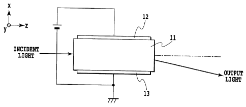
Embodiment 1
[0057]
Fig. 15 shows an electrooptic device of a parallel-plate
- 31 -
=
CA 02829445 2013-10-04
electrode type according to embodiment 1 of the present invention.
A KLTN crystal (in K1_yLiyTa1_xNbx03, x = about 0.40 and y =
about 0 . 001) is cut inthe shapeof arectangle, andanelectrooptic
crystal 11, of which four faces are polished, is prepared.
A positive electrode 12 and a negative electrode 13 made of
Ti/Pt/Au are formed on the upper face and the lower face of
the electrooptic crystal 11. The size of the electrooptic
crystal 11 is 6 mm (z axis) x 5 mm wide (y axis) x0.5 mm thick
(x axis), and the size of each electrode is 5 mm long x 4 mm
wide. In this specification, Ti/Pt/Au is used to indicate
that Pt and Au are laminated, in this order, on a lowermost
layer of Ti.
[0058]
The KLTN crystal is an electrooptic crystal having an
electrooptic constant that is great near the phase transition
from the cubic system to the tetragonal system. Since the
phase transition temperature of the KLTN crystal employed for
the embodiment 1 is 55 C, a Peltier device and a resistance
bulb are employed to set the temperature of this device to
60 C, which is higher by about 5 C than the phase transition
temperature. Thus, the Kerr effect can be employed as the
electrooptic effect of the KLTN crystal. As described above,
revealing the electrooptic effect of the electrooptic crystal
depends on the temperature inside the electrooptic crystal.
Therefore, temperature adjustment means should be provided
so that, in a case wherein the environmental temperature inside
the electrooptic device is not a temperature for revealing
- 32 -
CA 02829445 2013-10-04
the electrooptic effect of the electrooptic crystal, the
electrooptic crystal is maintained at a desired temperature.
[0059]
Light emitted by a He-Ne laser enters from one of the
end faces of the electrooptic crystal 11. So long as light
falls within the transmission area of the electrooptic crystal
11, an arbitrary wavelength can be applied. Using a polarization
plate and a half -wave plate, the polarized element of the incident
light is defined only as the element in the polarization axial
direction that is parallel to the electric field. The deflection
angle of the incident light is changed in consonance with a
direct-current voltage applied to the positive electrode 12
and the negative electrode 13. Fig. 16 shows a relationship
between the deflection angle of a deflected beam and the applied
voltage. The maximum deflection angle of 108 mrad, relative
to the applied voltage of +250 V, and the maximum deflection
angle of -85 mrad, relative to the applied voltage of -190
V, are obtained. That is, a deflection angle of almost 200
mrad in total can be provided.
[0060]
Fig. 17 shows a relationship between a current flowing
through the electrooptic crystal 11 and the applied voltage.
Since a current flowing through the electrooptic crystal 11
is non-linearly changed relative to the direct-current voltage
applied to the positive electrode 12 and the negative electrode
13, it can be said that the area of the electrooptic crystal
11 where the electric field is generated is in the space-charge
= - 33 -
CA 02829445 2013-10-04
limited state.
[0061]
When the above described simple and symmetrical structure,
which includes the rectangular electrooptic crystal 11 and
the parallel-plate positive electrode 12 and negative electrode
13, is employed, a large deflection angle that can not be provided
by a conventional electrooptic crystal prism can be obtained.
Furthermore, an alternating-current voltage may be applied
to the electrodes instead of a direct-current voltage to change
the deflection angle of a deflected beam in the time-transient
manner. The electrooptic device for the embodiment 1 can be
responsive within the range of a response frequency that is
determined based on the electrooptic constant (see non-patent
document 2) , and can respond to an alternating-current voltage
at a high frequency, equal to or higher than 1 kHz.
[0062]
Conventionally, a KTN (KTai,Nbx03, 0 < x < 1) crystal is
well known as a crystal that provides a great electrooptic
effect. The KTN crystal is formed like a prism, and when an
electric f ieldof 497 V/mm is applied to the KTNprism, a deflection
angle of about 10 mrad can be obtained (see non-patent document
3) . As for the electrooptic device of the embodiment 1, since
the deflection angle of about 100 mrad can be obtained upon
the application of a voltage of 250 V (an application of an
electric field of 500 V/mm) , the deflection efficiency can
be increased by ten times that obtained by the KTN prism described
in non-patent document 3.
- 34 -
CA 02829445 2013-10-04
Embodiment 2
[0063]
Fig. 18 shows qn electrooptic device of a horizontal
electrode type according to embodiment 2 of the present invention.
A KLTN crystal (in K1_yLiyTa1_xNb.03, x = about 0.40 and y
about 0.001) is cut into the shape of a rectangle, and an
electrooptic crystal 21 of which four faces are polished is
prepared. A positive electrode 22 and a negative electrode
23 madeofTi/Pt/Auare formedontheupperfaceof theelectrooptic
crystal 21. The size of the electrooptic crystal 21 is 6 mm
(z axis) x 5 mm wide (y axis) x 0.5 mm thick (x axis), and
the size of each electrode is 5 mm long.
[0064]
The KLTN crystal is an electrooptic crystal that has an
electrooptic constant that is great near the phase transition
from the cubic system to the tetragonal system. Since the
phase transition temperature of the KLTN crystal employed for
the embodiment 2 is 55 C, a Peltier device and a resistance
bulb are employed to set the temperature of this device to
60 C, which is higher by about 5 C than the phase transition
temperature. Thus, the Kerr effect can be employed as the
electrooptic effect of the KLTN crystal.
[0065]
Light emitted by a He-Ne laser enters through one of the
end faces of the electrooptic crystal 21. So long as light
falls within the transmission area of the electrooptic crystal
21, anarbitrarywavelengthcanbe applied. Usingapolarization
- 35 -
CA 02829445 2013-10-04
plate and a half -wave plate , the polarized element of the incident
light is defined only as the element in the polarization axial
direction that is parallel to the crystal surface on which
the electrode pair is formed. The deflection angle of the
incident light is changed in consonance with a direct-current
voltage applied to the positive electrode 22 and the negative
electrode 23. The maximum deflection angle of 16 mrad relative
to the applied voltage of 200 V is obtained. That is, a
deflection angle of almost 32 mrad in total can be provided.
[0066]
Fig. 19 shows a relationship between a current flowing
through the electrooptic crystal 21 and the applied voltage.
Since a current flowing through the electrooptic crystal 21
is non-linearly changed, relative to the direct-current voltage
applied to the positive electrode 22 and the negative electrode
23, it can be said that the area of the electrooptic crystal
21 in which the electric field is generated is in the space-charge
limited state.
[0067]
When the above described simple and symmetrical structure,
which includes the rectangular electrooptic crystal 21 and
one pair of the positive electrode 22 and negative electrode
23 formed on the crystal surface, is employed, a large deflection
angle that can not be provided by a conventional electrooptic
crystal prism can be obtained.
[0068]
In embodiments 1 and 2, one electrode pair of a positive
- 36 -
CA 02829445 2013-10-04
electrode and a negative electrode has been employed. However,
a plurality of electrode pairs may be employed so long as a
voltage by which a space-charge limited state is produced in
the electrooptic crystal can be applied. One, or two or more
alloys are selected from Ti, Pt, Au, Cu, Ag, Cr and Pd, and
the electrode pairs are formed by the individual alloy structure,
or by the alloy lamination structure.
Embodiment 3
[0069]
Fig. 20 shows a light beamdeflector according to embodiment
3 of the present invention. For the light beam deflector,
a positive electrode 32 and a negative electrode 33 are formed
on opposite faces of a block electrooptic crystal 31. The
electrooptic crystal 31, which is a KLTN crystal, is cut to
a size 6 mm long (z axis) x 5 mm wide (y axis) x 0.5 mm thick
(x axis), and electrodes 5 mm long x 4 mm wide are attached
to the opposite faces. The relative permittivity of the KLTN
crystal for this embodiment is 6300 at the measurement
temperature of 20 C. Ti/Pt/Au is employed as the electrode
material. Fig. 21 shows a distribution of the refractive index
change in the light beam deflector for the embodiment 3 of
the present invention. A distribution is shown for the
fluctuation, when a voltage applied between the positive and
negative electrodes is changed, of a refractive index of light
that vertically advances. The vertical axis represents the
change in a refractive index when no voltage is applied, and
the horizontal axis represents a distance from the positive
- 37 -
CA 02829445 2013-10-04
electrode.
[0070]
It is found that as the applied voltage is increased,
the refractive index near the positive electrode is greatly
changed, while the refractive index is nearly unchanged near
the negative electrode. That is, it is found that the ideal
ohmic contact (x0 = 0) shown in Figs. 8 and 9 is provided.
At the time of the applied voltage of 140 V, the inclination
of the refractive index is 1.5 x 10⁻³ per 1 mm. Since the length
of the electrode in the advancing direction of light is 5 mm,
the light wave plane is inclined at a rate of 7.5 x 10⁻³ mm
for the thickness of 1 mm. Therefore, at the time of the applied
voltage of 140 V, 7.5 mrad can be obtained as the deflection
angle relative to the light axis of the incident light.
Embodiment 4
[0071]
Fig. 22 shows the structure of a light intensity modulator
according to embodiment 4 of the present invention. An electrode
42 and a negative electrode 43 are formed on opposite faces
of an electrooptic crystal 41, and a deflector 44 is located
on the incidence side of the electrooptic crystal 41, while
an analyzer 45 is located on the emittance side. The electrooptic
crystal 41 is a KLTN crystal (in K1_yLiyTa1_xNb.03, x = 0.40 and
y= 0.001) . The positive electrode 42 and the negative electrode
43 made of Pt are formed on the upper face and the lower face
of the electrooptic crystal 41. The size of the electrooptic
crystal 41 is 6 mm long (z axis) x 5 mm wide (y axis) x 0.5
- 38 -
CA 02829445 2013-10-04
mm thick (x axis) , and the positive electrode 42 and the negative
electrode 43 are 5 mm long x 4 mm wide.
[0072]
The phase transition temperature of the KLTN crystal is
55 C, and the temperature of the electrooptic crystal 41 is
set to 60 C. A He-Ne laser beam is employed as incident light.
When a voltage of 58 V is applied between the positive and
negative electrodes, the polarization direction of output light
is rotated 90 degrees relative to the polarization direction
of incident light. As the voltage applied between the positive
electrode 42 and the negative electrode 43 is increased, turning
on and off the output light is repeated, so that a light intensity
modulator that has the operating characteristics shown in Fig.
3 can be obtained.
Embodiment 5
[0073]
Focusing on expression (19) described above, in a case
wherein the electrooptic device according to the mode of the
present invention is employed as a beam deflection device,
the deflection angle is proportional to the device length L
of the electrooptic device. Therefore, in order to obtain
a large deflection angle, the optical path of light passing
inside the electrooptic device need only be extended.
[0074]
Fig. 23A shows the structure of a beam deflector according
to embodiment 5 of the present invention. A KLTN crystal 51,
such that x = about 0.40 and y = about 0.001 for K1_yLiyTa1-xNbx03
- 39 -
CA 02829445 2013-10-04
is grown and cut to the shape of a rectangle, and four faces
are polished. A positive electrode 52 and a negative electrode
53 made of Ti/Pt/Au are formed on the upper face and the lower
face of the KLTN crystal 51. The size of the KLTN crystal
51 is 6 mm long in the light propagation direction (z axis) ,
mm wide (y axis) and 0.5 mm thick (x axis) . The electrodes,
formed on the upper and lower faces of the KLTN crystal by
vapor deposition, are 5 mm long in the light propagation
direction.
[0075]
Furthermore, mirrors 54 and 55, made of a metal such as
Au, or a dielectric multilayer f ilm are deposited on the incidence
face and the output face. Light emitted by a He-Ne laser enters,
as incident light, the KLTN crystal 51. Fig. 238 shows a beam
propagation path, viewed from the plane where the electrode
52 is formed. At this time, the angle in the direction horizontal
to the incidence plane of the KLTN crystal 51 is adjusted,
so that light passes through the inside of the crystal,
reciprocally, 1.5 times, i.e., passes between the incidence
plane and the output plane three times. As a result, the output
light is obtained.
[0076]
The KLTN crystal 51 is an electrooptic crystal having
an electrooptic constant that is great near the phase transition
from the cubic system to the tetragonal system. Since the
phase transition temperature of the KLTN crystal 51 is 55 C,
a Peltier device and a resistance bulb are employed to set
- 40 -
CA 02829445 2013-10-04
the temperature of this device at 60 C, which is higher by
about 5 C than the phase transition temperature. Thus, the
Kerr effect can be employed as the electrooptic effect for
the KLTN crystal 51.
[0077]
Fig. 24 shows a relationship between the applied voltage
of the beam deflector of embodiment 5 and the deflection angle.
When a voltage of 50 V is applied (an electric field of 100
V/mm is applied) between the positive electrode 54 and the
negative electrode 55, light is moved one time between the
incidence plane and the emittance plane, and the deflection
angle is about 7 mrad. Therefore, as shown in Fig. 23A, about
21 mrad is obtained as a deflection angle Div in the verical
direction (x axial direction) of output light.
Embodiment 6
[0078]
Fig. 25A shows the structure of a beam deflector according
to embodiment 6 of the present invention. A KLTN crystal 61,
such that x = about 0.40 and y = about 0.001 for K1_yLiyTa1_xNbx03,
is grown and cut to the shape of a rectangle, and four faces
are polished. A positive electrode 62 and a negative electrode
63 (not shown) made of Ti/Pt/Au are formed on the side faces
of the KLTN crystal 61. The size of the KLTN crystal 61 is
6 mm long in the light propagation direction (z axis) , 0.5
mm wide (y axis) and 5 mm thick (x axis) . The electrodes,
formed on the side faces of the KLTN crystal by vapor deposition,
are 5 mm long in the light propagation direction.
- 41 -
CA 02829445 2013-10-04
[0079]
Furthermore, mirrors 64 and 65, made of a metal such as
Au, or a dielectric multilayer film are deposited on the incidence
face and the emittance face. Light emitted by a He-Ne laser
enters, as incident light, the KLTN crystal 61. Fig. 25B shows
a beampropagat ion path, viewed from the plane where the electrode
62 is formed. At this time, the angle in the direction
perpendicular to the incidence plane of the KLTN crystal 61
is adjusted, so that light is output after passing through
the inside the crystal, reciprocally, 2.5 times, i.e., passes
between the incidence plane and the emittance plane five times.
[0080]
The KLTN crystal 61 is an electrooptic crystal having
an electrooptic constant that is great near the phase transition
from the cubic system to the tetragonal system. Since the
phase transition temperature of the KLTN crystal 20 is 55 C,
a Peltier device and a resistance bulb are employed to set
the temperature of this device at 60 C, which is higher by
about 5 C than the phase transition temperature. Thus, the
Kerr effect can be employed as the electrooptic effect for
the KLTN crystal 61.
[00811
When a voltage of 150 V is applied (an electric field
of 200 V/mm is applied) between the positive electrode 62 and
the negative electrode 63, light is moved one time between
the incidence plane and the emittance plane, and the deflection
angle is about 30 mrad. Therefore, about 150 mrad is obtained
- 42 -
CA 02829445 2013-10-04
as a deflection angle 22 in the horizontal direction (y axial
direction) of an output beam 21.
[0082]
According to embodiment 5 and embodiment 6, since the
optical path of light that passes inside the electrooptic device
is extended, a drive voltage can be set to 1/qn (n: passage
count) , compared with a case wherein, one time only, light
passes through the inside the electrooptic device having the
same device length. When the drive voltage is the same, the
device length of the electrooptic device can be reduced to
1/n. As the device length is shorter, the capacitance element
becomes smaller relative to the voltage to be applied, and
the speed of the deflection operation can be increased.
Furthermore, the quadratic electrooptic constant sii is greater
for a case sii wherein the light polari zat ion direction is parallel
to the applied electric field than for a case sii wherein the
light polarization direction is perpendicular to the applied
electric field. Therefore, when the number of times
reciprocation is increased, a satisfactory deflection angle
can be obtained.
[0083]
It. should be noted that mirrors may be provided by forming
a metal or a dielectric multilayer film through vapor deposition
or sputtering, or by using total reflection on the end face
of the crystal.
Embodiment 7
[0084]
- 43 -
CA 02829445 2013-10-04
Fig. 26 shows the structure of a beam deflector according
to embodiment 7 of the present invention. A KLTN crystal 71
such that x = about 0.40 and y = about 0.001, for K1_yLi7Ta1_xNbx03,
is grown and cut to the shape of a rectangle, and four faces
are polished. A positive electrode 72 and a negative electrode
73 made of Ti/Pt/Au are formed on the upper face and the lower
face of the KLTN crystal 71. = The positive electrode 72 and
the negative electrode 73 serve as vertical deflection electrodes .
Further, a positive electrode 74 and a negative electrode
75, which serve as horizontal deflection electrodes, are formed
on the side faces of the KLTN crystal 71. Furthermore, mirrors
76 and 77 made of metal or a dielectric multilayer film are
deposited on the incidence face and the emittance face.
[0085]
Light emitted by a He-Ne laser enters, as incident light,
the KLTN crystal 71. At this time, the angles in the directions
horizontal and perpendicular to the incidence plane of the
KLTN crystal 71 are adjusted, so that light is output after
it has passed through the inside the crystal, reciprocally,
2.5 times, i.e., is passed between the incidence plane and
the emittance plane five times. As a result, as well as in
embodiment 5 and embodiment 6, the output light can be deflected
horizontally and vertically.
Embodiment 8
[0086]
Fig. 27 shows a two-dimensional beam deflector according
to embodiment 8 of the present invention. Electrooptic crystals
- 44 -
CA 02829445 2013-10-04
having a size 6 mm long x 5 mm wide x 0.5 mm thick are cut
from a KLTN crystal. Electrodes 5 mm long x 4 mm wide are
attached to opposite faces 82 and 83, and 92 and 93 of electrooptic
crystals 81 and 91, respectively. The phase transition
temperature of the KLTN crystal is 55 C, and the temperature
of the electrooptic crystals 81 and 91 is set at 60 C. Cr is
employed as the electrode material. The electrooptic crystals
81 and 91 are located on the optical path, so that the direction
in which the electric field is to be applied to the electrooptic
crystal 81 is at a right angle to the direction in which the
electric field is to be applied to the electrooptic crystal
91. A half-wave plate 101, made of rock crystal, is inserted
into the optical path between the electrooptic crystals 81
and 91, so that light output by the electrooptic crystal 81
is to be rotated 90 degrees and enter the electrooptic crystal
= 91.
[0087]
As described above, the deflection efficiency depends
on the field direction of light, and reaches the maximum when
the field direction for light is parallel to the space field
direction due to the applied voltage. Therefore, based on
the polarization dependency, the tilt of the refractive index
change is different between vertically polarized light and
horizontally polarized light. According to the KLTN crystal,
since s11:s1.2 = about 10:-1 is the Kerr constant relative to
vertically polarized light (the y axial direction in Fig. 27)
and horizontally polarized light (the x axial direction in
- 45 -
CA 02829445 2013-10-04
Fig. 27) , only the output angle of vertically polarized light
is greatly changed.
[0088]
Thus, in the electrooptic crystal 81, light is deflected
in the y axial direction by applying an electric field in parallel
to vertical ly polari zed 1 ight , and the deflected light is rotated
90 degrees by the half-wave plate 101. And in the electrooptic
crystal 91, the resultant light is deflected in the x axial
direction by applying an electric field that is parallel to
horizontally polarized light. As a result, efficient
two-dimensional deflection is enabled.
Embodiment 9
[0089]
Fig. 28 shows the structure of a two-dimensional beam
deflector according to embodiment 9 of the present invention.
An electrooptic crystal, which is a KLTN crystal, is cut out
to obtain a size 20 mm long x 5 mm wide x 5 mm thick, and is
shaved to obtain an octagonal prism whose longitudinal cross
section is an octagon. Three pairs of electrodes 5 mm long
x 1.5vmm wide are attached to opposite faces of an electrooptic
crystal 111. The phase transition temperature of the KLTN
crystal is 55 C, and the temperature of the electrooptic crystal
111 is set at 60 C. As for the electrodes, beginning with the
light incidence side, electrodes 122 and 123 for a first deflector,
electrodes 132 and 133 for a half-wave plate and electrodes
142 and 143 for a second deflector are sequentially attached.
[0090]
- 46 -
CA 02829445 2015-08-07
Here, Cr is employed as the electrode material for the
electrodes 122 and 123 and the electrodes 142 and 143, and
Pt is employed as the electrode material for the electrodes
132 and 133. For the deflector electrodes, the electron
injection efficiency must be increased in order to improve
the deflection efficiency, and an electrode material that will
serve as an ohmic contact should be selected. On the other
hand, for the electrodes for a half-wave plate, since simply
the rotation of a polarized wave is required, no occurrence
of deflection is preferable . Therefore, the electron inj ection
efficiency must be reduced, and an electrode material that
serves as a Schottky contact should be selected.
[0091]
With this arrangement, as well as in embodiment 8, light
is deflected by the first deflector in the y axial direction,
and the deflected light is rotated 90 degrees by the half-wave
plate. And the resultant light is deflected by the second
deflector in the x axial direction. Since as described above
a single KLTN crystal is employed to provide three functions,
i.e., a vertical deflection function, a horizontal deflection
function and a half-wave plate, a KLTN crystal for a cubic
system is preferable.
Embodiment 10
[0092]
Fig. 29A shows the structure of a two-dimensional beam
deflector according to embodiment 10 of the present invention.
An electrooptic crystal 201, which is a KLTN crystal, is cut
- 47 -
CA 02829445 2015-08-07
to obtain a size 10 mm long (z axis) x 5 mm wide (y axis) x
0.5 mm thick (x axis). Two pairs of electrodes are attached
to opposite faces of the electrooptic crystal 201. Beginning
from the light incidence side, electrodes 202 and 203 for a
first deflector and electrodes 204 and 205 for a second deflector
are attached. There is no problem in replacing this order.
The phase transition temperature of the KLTN crystal is 55 C,
and the temperature of the electrooptic crystal 201 is set
at 60 C.
[0093]
The electrodes 202 and 203 of the first deflector are
shaped like right-angled triangles employing, as the base,
the side near the incidence of light. One of the base angles
is a right angle, the other base angle (I) is 30 degrees, the
length of the base is 4 mm, the height is 3 mm, and the length
of the hypotenuse is 5 mm. For the electrodes 202 and 203
of the first deflector, an electrode material containing Pt
is employed, so that a Schottky contact is obtained. The
electrodes 204 and 205 for the second deflector are rectangular
electrodes 5 mm long x 4 mm wide. For the electrodes 204 and
205 of the second deflector, an electrode material containing
Ti is employed, so that an ohmic contact is obtained.
[0094]
Since, through the electrooptic effect provided by the
KLTN crystal, the refractive index is uniformly changed in
the portion in which the electrodes 202 and 203 for the first
deflector are formed, this portion serves as a prism that acts
- 48 -
CA 02829445 2013-10-04
on incident light. When n denotes the refractive index of
the electrooptic crystal 201, Sii denotes an electrooptic
constant, d denotes a thickness, V denotes an applied voltage,
and 4) denotes the base angle of one of the electrodes 202 and
203 for the first deflector, the deflection angle is represented
by
[0095]
[Expression 171
v 2
=-1n3S..(1-) tan0 (20)
2 d
and light is deflected in the y axial direction.
[0096]
As well as in embodiment 3, the ideal ohmic contact is
provided in the portion wherein are located the electrodes
204 and 205 for the second deflector, and the charge injection
efficiency is the maximum. Therefore, since output light is
-= = deflected in the x axial direction, efficient two-dimensional
deflection is enabled.
Embodiment 11
[0097]
.At present, a three-axis lens actuator is employed for
a servo mechanism employed for an optical recording/reproduction
apparatus used for DVDs. The actuator employs a moving coil
motor to drive a wire that holds an object lens. The Lorentz
force that acts on charges that move through magnetic fluxes
is employed as the driving principle of the moving coil motor.
Since this actuator mechanism is a mechanically operated type,
- 49
CA 02829445 2013-10-04
many inherent vibration modes are included. In a case wherein
the actuator is driven at a frequency equal to the inherent
vibrations, an inherent mode is driven and resonance occurs.
The lowest order resonance of the actuator can be avoided
through the control exercised by a control system. However,
it is difficult to avoid the affect by a higher-order resonance,
and as a result, a high-order resonance is not stabilized by
the control system, and accurate positioning is difficult.
Therefore, the above described light beam deflector is employed
to provide an optical pickup apparatus that comprises a servo
mechanism that does not include a mechanically driven portion.
[0098]
Fig. 30 shows the arrangement of an optical pickup apparatus
according to embodiment 11 of the present invention. The optical
pickup apparatus employs the light beam deflector shown in
Fig. 20 for the embodiment 3, and recording media are ]JVDs
and HD-DVDs. A light beam emitted by a DVD laser diode (LD)
311, which is a light source, is passed through a half mirror
312 and a collimating lens 313 and enters an optical deflection
device 314. Based on a tracking signal reflected by a disk
316, a controller (not shown) provides feedback control for
the deflection angle at the optical deflection device 314.
The light beam output by the optical deflection device 314
is transmitted via an object lens 315 to irradiate the disk
316.
[0099]
An optical signal reflected by the disk 316 passes through
- 50 -
CA 02829445 2013-10-04
the half mirror 322 and a detection lens 323, and enters a
photodiode (PD) 324. Further, an HD-DVD laser diode (LD) 321
is optically coupled with the half mirror 322.
[0100]
As described above, according to the conventional method,
an object lens is driven by an actuator. Since the optical
deflection device of this mode does not include a moving portion,
resonance due to the driving of the main body does not occur.
On the other hand, since a material that provides the quadratic
electrooptic ef fect is employed, the resonance phenomenon occurs
in the device material due to an electrostriction effect.
Since this phenomenon depends on the size and shape of the
material, the occurrence of the phenomenon can be controlled
by breaking the symmetry of the shape. In this mode, the band
of the servo has been defined as 1 MHz, at which the stable
operation can be satisfactorily performed and optical
recording/reproduction of high quality enabled. Since a
= voltage at this time for driving the optical deflection device
to deflect a light beam falls within the range of 12 V, the
optical deflection device can be driven at a voltage that is
satisfactory for practical use.
[010].]
Further, the optical deflection device has been located
between the collimating lens 313 and the object lens 315.
However, so long as the location is along the optical path
between the light source and a recording medium, the optical
deflection device may be arranged at other portions of the
- 51 -
CA 02829445 2013-10-04
optical pickup apparatus to obtain the same effects.
Furthermore, since the light transmission wavelength of the
optical deflection device is within a range of from 400 nm
to 4000 nm, the device can be applied for an optical pickup
apparatus that employs a plurality of wavelengths of visible
light.
[0102]
The optical pickup apparatus that employs the light
deflection device of this mode has a band wherein appropriate
control can still be exercised for a case wherein recording
and reproduction at a high density, such as a 1TB class, is
performed. Therefore, when the apparatus is employed for an
HD-DVDorBlu-raythatrequireshigherdensityrecording, greater
effects can be anticipated, and higher-density
recording/reproduction can be provided.
= Embodiment 12
[0103]
For performing printing, a laser printer radiates a
photosensitive member with a laser beam, attaches toner to
the exposed portion, and transfers the toner to a recording
sheet. At this time, it is required that a laser beam be
repetitively deflected, at least in the direction of one axis.
The above described technique for rotating a polygon mirror
is employed as a light deflection technique. For an improvement
in the printing speed of a printer, a higher-speed optical
deflection technique is requested. Thus, the above described
light beam deflector is employed to provide a fast laser printer.
- 52 -
CA 02829445 2013-10-04
[0104]
Fig. 31A shows the structure of a laser printer according
to the mode of the present invention. The illustrated laser
printer employs the light beam deflector shown in Fig. 20 for
embodiment 3. For comparison, a conventional laser printer
is shown in Fig. 31B. In the laser printer, a charging unit
412, a developing unit 415, a transfer unit 414 and a fixing
unit 413 are arranged around the periphery of a cylindrical
photosensitive drum 411, which is a photosensitive member.
The photosensitive drum 411 charged by the charging unit 412
is irradiated by a laser beam, and toner is attached to the
exposed portion by the developing unit 415. Then, a toner
image is transferred to a recording sheet 416 by the transfer
unit 414, and is fixed by the fixing unit 413.
10105]
=
As shown in Fig. 31B, in a conventional laser printer,
a laser beam emitted by a laser diode 431 is collimated by
a collimating lens 432, and is reflected by a polygon mirror
433. The laser beam is deflected by rotating the polygon mirror
433, and the deflected beam is transmitted via a lens 434 to
radiate a photosensitive member 411. As shown in Fig. 31A,
in the laser printer of this mode, a laser beam emitted by
a laser diode 421, which is a light source, is collimated by
a collimating lens 422, and enters an optical deflection device
423. The laser beam deflected by the optical deflection device
423 is transmitted via a lens 424 to radiate the photosensitive
member 411.
- 53 -
CA 02829445 2013-10-04
[0106]
For the optical deflection device 423 located on the optical
path extending between the laser diode 421 and the photosensitive
member 411, four elements are employed in order to scan the
entire photosensitive member 411 in the scanning direction.
Since the power consumed by one element is equal to or lower
than 1 mW, power consumption is reduced compared with the
conventional laser printer. Further, since the chip size of
the optical deflection device is so small that it can be integrated
with a laser diode, downsizing is enabled, unlike the polygon
mirror.
[0107]
The optical deflection speed of the optical deflection
device 423 is 1 MHz, and the maximum rotation frequency of
the polygon mirror 433 is 10 kHz (60000 rpm) . Assuming that
the polygon mirror 433 has ten mirror planes, the laser printer
for this mode can provide ten times the speed. For example,
a conventional fast laser printer that employs a plurality
of laser beams has a printing capability of about 40 sheets
per minute, while the laser printer of this embodiment can
obtain a printing capability of about 300 sheets per minute.
10108]
Furthermore, two optical deflection devices, the field
directions of which intersect each other, are located and a
half-wave plate is arranged between the two optical deflection
devices. When the two optical deflection devices are controlled
separately, two-dimensional scanning by a laser beam can be
- 54 -
=
CA 02829445 2013-10-04
performed. Since the speed of the exposing of the photosensitive
member can be remarkably increased through two-dimensional
scanning, a printing capability of about 500 sheets per minute
can be obtained. Further, when one more optical deflection
device is located between the optical deflection devices and
the laser diode, and when light is deflected outside the optical
path used for exposure by a laser beam, a light ON/OFF function
can be additionally provided.
- 55 -