Note: Descriptions are shown in the official language in which they were submitted.
1
CONTROLLED FABRICATION OF NANOPORES IN
NANOMETRIC SOLID STATE MATERIALS
[0001]
STATEMENT REGARDING FEDERALLY SPONSORED RESEARCH
[0002] This invention was made with Government support under
Contract No. R01HG003703, awarded by the National Institutes of Health.
The Government has certain rights in the invention.
BACKGROUND
[0003] This invention relates generally to nano-scale fabrication
techniques, and more particularly relates to techniques for producing
nanopores in nanometric solid state materials.
[0004] Nanometric solid state materials, that is, solid state
materials
that can exist in equilibrium with only nanometers in thickness, include a
wide range of materials such as monolayer, few-monolayer, and single
molecule materials, that are becoming increasingly important for a wide range
of applications, including, e.g., electronic, biological, and chemical
applications. Many such applications require high-precision nanoscale
features and structures for operation. For example, well-defined nanopores, or
nanoscale pores having a diameter less than about 100 nanometers, are
particularly required for many applications due to the nano-scale of the
application itself or the environment in which the nanopore is to operate.
[0005] For example, nanopore-articulated nanoscale devices are of
great
interest for enabling the localization, detection, and characterization of
molecules such as single DNA molecules or protein molecules. Nanopore
CA 2829833 2018-07-13
CA 02829833 2013-09-10
WO 2012/125770
PCT/US2012/029132
2
filters and nanoscale holely membranes are likewise important for many
critical biological separation and characterization procedures, as well as
filtration processes. Many other micro-fluidic and nano-fluidic processing and
control applications similarly rely on nano-scale features in nanometric
materials.
100061 To produce a nanoscale structure such as a nanopore in a
nanometrically-thin material, it is in general required to manipulate the
material with the precision of single atoms. This is in contrast to most
conventional microelectronic fabrication processes, which characteristically
only require precision that approaches the micron-scale. But without feature
resolution and fabrication precision at the atomic level, it has in general
not
been possible to manipulate nanometrically-thin materials in a manner that
exploits the particular characteristics which emerge at the nano-scale.
100071 High-precision nanoscale processing has historically required a
one-at-a-time fabrication paradigm that is often costly and inefficient.
Generally, the high-volume, batch fabrication techniques of conventional
microelectronic production have been incompatible with nanoscale feature
production and material manipulation. But without the ability to precisely,
reproducibly, and inexpensively mass-produce nanoscale features such as
nanopores, many nanoscale systems cannot be developed for commercial
implementation of many important nanoscale applications.
SUMMARY OF THE INVENTION
100081 There is provided a method and corresponding structures that
overcome the limitations of previous processes to controllably form nanopores.
In one example method of forming a nanopore in a nanometric material, a
nanopore nucleation site is formed at a location of the nanometric material
that is interior to lateral edges of the material by directing a first
energetic
beam, selected from the group of ion beam and neutral atom beam, at the
interior location for a first time duration that imposes a first beam dose
which
3
causes removal of no more than five interior atoms from the interior location
to produce at the interior location a nanopore nucleation site having a
plurality of edge atoms. A nanopore is then formed at the nanopore
nucleation site by directing a second energetic beam, selected from the group
consisting of electron beam, ion beam, and neutral atom beam, at the
nanopore nucleation site with a beam energy that removes edge atoms at the
nanopore nucleation site but does not remove bulk atoms from the nanometric
material.
[0008.1] In an embodiment, there is provided a method of forming a
nanopore in a nanometric material, the method comprising:
forming a nanopore nucleation site at a location of the nanometric
material that is interior to lateral edges of the material by directing a
first energetic beam, that is an ion beam or a neutral atom beam, at the
interior location with a beam energy that is at least that beam energy
which provides at the nanometric material a bulk atom displacement
energy of Edbulk, that can remove bulk atoms from the nanometric
material, for a first time duration that imposes a first beam dose which
causes removal of no more than five interior bulk atoms from the
interior location to produce at the interior location a nanopore
nucleation site having a plurality of edge atoms; and
forming a nanopore at the nanopore nucleation site by directing a
second energetic beam, that is an electron beam, ion beam, or a neutral
atom beam, at the nanopore nucleation site with a beam energy that is
less than that beam energy which provides at the nanometric material
a bulk atom displacement energy of &bulk, to thereby remove edge
atoms at the nanopore nucleation site but not remove bulk nanometric
material atoms that are not at the nanopore nucleation site.
[0009] With the methods described herein, there can be produced a
nanometric structure with nanopores. The structure is formed of an
.. impermeable self-supporting nanometric material having a thickness of no
CA 2829833 2018-07-13
3a
greater than about 5 nm. In the nanometric material is a plurality of
nanopores of at least about 1000 nanopores/cm2. Each of the nanopores has a
diameter that is no greater than about 10 nm. The plurality of nanopores is
monodisperse in diameter with a variation of about 30%.
[0009.1] In an embodiment, there is provided nanometric structure
comprising:
an impermeable self-supporting nanometric material of graphene, few-layer
graphene, fluorographene, graphane, or graphene oxide, having a thickness of
no greater than about 5 nm; and
a plurality of nanopores in the nanometric material of at least 1000
nanopores/cm2, each nanopore having a diameter no greater than 10 nm and
the plurality of nanopores being monodisperse in diameter with a variation of
30%.
[0009.2] In a further embodiment, there is provided a nanometric
structure comprising:
an impermeable self-supporting nanometric material of graphene, few-layer
graphene, fluorographene, graphane, or graphene oxide, having a thickness of
no greater than 5 nm; and
a plurality of nanopores in the nanometric material of at least 50 nanopores,
each nanopore having a diameter no greater than 10 nm and the plurality of
nanopores having a monodispersity in diameter of 30%.
[0010] The nanometric structures of nanopores described herein, and
the method for producing the nanopores described herein, enable a wide range
of micro-fluidic and nano-fluidic applications, including molecular detection
and analysis, fluidic filtering and separation, and fluidic reactions.
[0011] Other features and advantages will be apparent the following
description and accompanying figures, and from the claims.
BRIEF DESCRIPTION OF THE DRAWINGS
[0012] Fig. 1 is a flow chart of a two-step process for producing a
nanopore in a nanometric material;
CA 2829833 2018-07-13
3b
[0013] Figs. 2A and 2B schematic views of nanometric materials
disposed across an opening on a support frame and disposed across an array of
openings on a support frame, respectively, for carrying out the method of the
flow chart of Fig. 1;
CA 2829833 2018-07-13
CA 02829833 2013-09-10
WO 2012/125770
PCT/US2012/029132
4
100141 Figs. 3A-3E are schematic side views of a nanometric material
as
the nanometric material is processed in the steps of the flow chart of Fig. 1;
100151 Fig. 4 is a schematic side view of a patterned shielding
material
employed to selectively mask a nanometric material during the nanopore
fabrication process of the flow chart of Fig. 1;
100161 Figs. 5A-5B are schematic views of nanopores formed in
nanometric materials disposed across an opening on a support frame and
disposed across an array of openings on a support frame, respectively,
produced by the method of the flow chart of Fig. 1;
100171 Fig. 6A is a plot of average nanopore radius as a function of
electron dose for five experimental nanopores;
100181 Fig. 6B is a plot of nanopore radius as a function of electron
dose
for each of the nanopores from which data was taken for the plot of Fig. 6A;
100191 Fig. 7 is a an electron micrograph of a region of graphene in
which an array of nanopores has been formed by the method of the flow chart
of Fig. 1; and
100201 Fig. 8 is a plot of the distribution of nanopore radius for the
electron micrograph of Fig. 7.
DETAILED DESCRIPTION
100211 Referring to Fig. 1, a process 10 for controllably forming one or
more nanopores can in general be implemented in a nanometric material with
the two steps shown therein. In a first step 12, at least one nanopore
nucleation site is produced at a selected location or at multiple selected
locations in a nanometric material for which the controlled fabrication of a
nanopore is desired. Then in a second step 14, a nanopore is controllably
formed at the nucleation site or sites. Each of these steps is described in
detail below.
100221 This two-step nanopore formation method can be applied to any
suitable material, but is particularly well-suited for producing nanopores in
a
CA 02829833 2013-09-10
WO 2012/125770 PCT/US2012/029132
solid state material or structure that is characterized by a thickness that is
nanometric, and for many applications, that is less than about 5 nanometers
in thickness or less than 3 nanometers in thickness. Such nanometric
materials include, e.g., atomically-thin materials, which in general can be
5 described as materials having a thickness of an atomic monolayer or a few
atomic layers, such as a monolayer, a bilayer, or a trilayer of atoms. A mono-
atomically-thick material is herein defined as a material which is one atom in
thickness, but need not be atoms of just one element. Atoms of a plurality of
different elements can be included in an atomic layer. The mono-atomically-
thick layer can be decorated at the layer top and/or bottom with heterogeneous
atoms and other species that do not lie in the plane of the atoms. Such
atomically-thin materials include, e.g., two-dimensional free-standing atomic
crystals, and other structures having a characteristic unit, like a lattice
constant, that is repeating in two dimensions but not the third. Atomically-
thin materials also include non-crystalline materials, such as glassy
materials
for which a mono-atomic layer and few-atomic-layers can be formed. Other
example nanometric materials include materials that are a single molecule in
thickness, or that are two or three molecules in thickness.
100231 Examples of nanometric materials that are well-addressed by the
method include graphene, few-layer graphene, fluorographene, graphane,
graphene oxide, hexagonal boron nitride (hexagonal-BN), mono-atomic glasses,
and other such materials. Other suitable materials include, e.g., MoS2, WS2,
MoSe9, MoTe2, TaSe2, NbSe2, NiTe2, Bi2Sr2CaCu20x, and Bi2Te3. These are
representative examples of suitable nanometric solid state materials but are
not limiting; any suitable material in which one or more nanopores are to be
formed can be employed.
100241 In the method, a selected nanometric material is provided in a
suitable configuration for processing to produce one or more nanopores in the
material. The nanometric material is preferably arranged such that one or
CA 02829833 2013-09-10
WO 2012/125770 PCT/US2012/029132
6
more energetic species can be directed through the material for both producing
a nanopore nucleation site and for controllably forming a nanopore at the
site,
as explained in detail below. For many applications, it can be convenient to
arrange the nanometric material on a continuous or discontinuous underlying
support structure in any convenient orientation that accommodates such
nanopore processing. The support structure can be discontinuous, with a
topology and material configuration depending on an intended application,
and can serve as a masking material, patterned with, e.g., openings of a
selected masking pattern, as described below. The nanometric material in
which a nanopore is to be formed can be, e.g., self-supporting, with support
at
lateral edges near or at the periphery of the material or at locations within
at
interior points, or in another configuration that accommodates the direction
of
an energetic species through the nanometric material. The nanometric
material can be synthesized in-position, e.g., in situ in a device or system
configuration, on a selected support structure, or can be produced or
synthesized fully or partially elsewhere and then transferred to the selected
support structure.
100251 The support structure can be provided as any suitable support
material, including microelectronic materials and substrates that are
electrically conducting or electrically insulating. The support structure can
be
provided as a bulk structure having the composition of the nanometric
material or can be provided as a heterogeneous combination of materials. In
one example, a support structure is provided as a frame and the nanometric
material in which one or more nanopores are to be produced is transferred to
the frame.
100261 For example, a silicon substrate can be configured as a support
with a frame membrane, e.g., a silicon nitride or other material frame
membrane, having one or more apertures in the frame membrane. As shown
in Fig. 2A, the nanometric material 16 can be positioned over the frame
CA 02829833 2013-09-10
WO 2012/125770 PCT/US2012/029132
7
membrane 18 on the substrate 20. The frame membrane 18 thereby operates
as a support frame around the aperture 22, to enable a self-supported region
24 of nanometric material across the aperture 22. As shown in Fig. 2B, this
arrangement can be extended to accommodate any number of distinct areas of
nanometric material that are each suspended 24 in an array 26, disposed in a
support frame 28 across apertures in the frame membrane on a substrate.
100271 In general, the apertures provided in a support frame membrane
layer can be, e.g., rectangular, circular, or of another suitable geometry,
and
can be, e.g., between about 5 - 10 nm and about 200 nm in extent or other
geometry and extent corresponding to a selected nanopore size and location, as
explained in more detail below. For many applications, it can be preferred
that the aperture in the support frame membrane be at least about ten times
greater than the nanopore to be formed in the nanometric material.
100281 In a further example, a transmission electron microscopy (TEM)
grid can be employed as a support frame for a nanometric material to be
processed. The TEM grid can be covered with a suitable material, such as a
thin amorphous carbon film, and one or more holes, or an array of holes, can
be formed in the film to provide a frame for the nanometric material. Other
such arrangements can be employed and no particular support or frame is
required.
100291 Where the nanometric material is synthesized separately from a
support or frame, the material can be transferred to a support or frame at a
convenient juncture in the synthesis process. In one example, a single layer
of
graphene or few-layer graphene is synthesized and once synthesized, is
transferred to a selected support structure. In this example, the graphene can
be synthesized by a suitable process, e.g., a chemical vapor deposition
process
(CVD), or by ion implantation or gas phase synthesis, or by another synthesis
technique on a suitable structure, e.g., a metal layer or substrate, or can be
produced by exfoliation of graphite, in the conventional manner.
Alternatively,
CA 02829833 2013-09-10
WO 2012/125770 PCT/US2012/029132
8
the material can be synthesized by a suitable process, e.g., (CVD), ion
implantation, or another synthesis technique, on a suitable structure, e.g., a
metal layer or substrate, after which the structure, e.g., a metal layer or
substrate, can be converted into a support structure for the nanometric
material by some method, such as a patterned chemical etching, that does not
affect the nanometric material through which nanopores are subsequently to
be formed. No particular nanometric material synthesis process is required,
and the nanometric material to be processed, such as graphene, can be
produced in any suitable manner.
100301 In one particularly convenient graphene synthesis process, a
nickel or copper foil can be annealed at a low pressure at a temperature of,
e.g.,
about 1000 C, for about 10 minutes, under the flow of H2, and then also
exposed to flow of CH4 for about 10 minutes at 1000 C, to grow a region or
regions of graphene. At the end of the 10 minute growth step, the foil is
cooled
to room temperature with flow of H2, in a process which takes about 2 hours.
100311 If the nanometric material to be processed is produced on a
synthesis structure, such as the graphene synthesis on copper foil just
described, then it is preferred that the nanometric material be well-cleaned
and, if the nanometric material is to be transferred, that this transfer
proceed
with great care so as not to damage or contaminate the nanometric material.
For example, once graphene is synthesized on a copper foil, a suitable piece
of
graphene on the foil can be punched out and placed on an acid-washed clean
glass slide for handling during transfer to a support structure. Polymer-based
handle materials can alternatively be employed. Where the support structure
is, e.g., a TEM grid having a holely carbon layer, a droplet of deionized
water
or other suitable liquid is first placed on the grid layer, and then when
brought into contact with the graphene, the carbon film is pulled into
intimate
contact with the graphene by the receding interface from the liquid. A glass
CA 02829833 2013-09-10
WO 2012/125770 PCT/US2012/029132
9
slide can be placed on top of the TEM grid to enable application of force
during
the contact.
100321 The copper film on which the graphene was synthesized can then
be etched away from below by, e.g., floating the structure on a suitable
etchant,
e.g., a copper etchant including FeCl3 for a suitable duration, e.g., 15
minutes
for a 25 gm-thick foil. If over-etched, the FeCl3 will attack the TEM grid at
locations where the grid is exposed at carbon layer edges. Similarly, a
polymer film can be removed after placement of the graphene. Once the
copper film or other material is removed, the graphene as-positioned on the
TEM grid can be cleaned, e.g., by floating the structure in 1 N HC1, to remove
residual iron from the FeCl3 exposure, for about 10 minutes, and then floated
in multiple rinses of deionized water, for example, about three rinses of ten
minutes each, to remove any residual salt, and dried in dry nitrogen.
100331 For many nanometric materials in which a nanopore is to be
formed, e.g., graphene, a high degree of cleanliness is especially preferred,
specifically, with regard to graphene, e.g., to reduce the density of
hydrocarbon contaminants such that mobile hydrocarbons on the graphene
surface are substantially reduced. This high degree of cleanliness can be
preferred for aiding in the nanopore formation process. Therefore, if after
the
cleaning and rinsing process described above it is found that some amount of
surface contamination remains, it can be preferred to conduct a further
cleaning step.
100341 In one example cleaning process, contaminants are baked out of
the structure. Here the TEM grid with, e.g., a graphene layer affixed as
described above, is transferred to a stainless steel ultra high vacuum (UHV)
chamber, and at a pressure of, e.g., less than about 10-8 Torr, the
temperature
is ramped to about 300 C. The structure is then baked for at least two hours,
and preferably overnight, at this temperature. The chamber is then cooled to
room temperature slowly, e.g., at less than about 2 C/min, with a final
CA 02829833 2013-09-10
WO 2012/125770
PCT/US2012/029132
chamber pressure at between, e.g., about 10-8 T and about 10-9 T. It is
preferred that the structure be stored at room temperature under UHV
conditions until use. This process is found to produce a graphene surface that
is about 40% - 80% free of any contaminating material, as-observed by TEM
5 viewing.
100351 This example demonstrates that in general, it is preferred to
maintain the nanometric material to be processed under optimally clean
conditions, so that atomic-scale processing of the material is not affected by
contaminants. No particular cleaning or storage processes are required, and
10 those processes best-suited to a selected material are preferred. With a
selected material in place on a support structure, the method for controllably
producing a nanopore can be carried out.
100361 Referring to Fig. 3A, there is shown a nanometric material 30
to
be processed for the production of nanopores, arranged such that a plane of
atoms 32 of the material is accessible. In this example illustration, one
layer
of atoms is shown for clarity in explaining the process steps, but such is not
required; as explained above, the nanometric material can be an atomic
multilayer material, a molecular monolayer material, or other nanometric
material having a thickness that is generally less than about 5 nm.
100371 With the nanometric material in such an arrangement, in the
first method step, one or more nanopore nucleation sites are formed in the
nanometric material at locations that are interior to the lateral edges of the
nanometric material, and at which nanopores are to be formed. At such an
interior nanopore nucleation site, some disruption to the continuity of the
nanometric material is provided that produces edges of material from which
edge atoms can be removed for controllably forming a nanopore of a selected
size. In other words, due to a disruption in the nanometric material, interior
atoms are rendered as edge atoms for removal in the process of forming a
nanopore. Each nanopore nucleation site is therefore a site at an interior
CA 02829833 2013-09-10
WO 2012/125770
PCT/US2012/029132
11
location of the nanometric material where edge atoms are produced by the
nucleation site formation.
100381 To form a nanopore nucleation site, some perturbation of the
nanometric material atoms is required. In one example of such, a structural
defect or a single cluster of defects is formed in the nanometric material at
a
location interior to lateral edges of the material. The defect can be created
by,
e.g., displacing a single atom or small number of atoms in the material or
otherwise disrupting the atomic structure of the material. The term "defect"
is therefore here intended to refer to an aberration in the atomic bonding
structure of the nanometric material. For example, given the nanometric
material graphene, a defect can be created by the removal of one or two atoms
from the sp2 bonded graphene carbon network of the material. A sufficient
defect exists in the material when the number of bonds holding one or more
atoms in place is altered and/or reduced and the defect is relatively stable
at a
.. selected operating temperature. A one or two atom defect in a hexagonal
lattice such as that of graphene can produce three ¨ four edge atoms at the
site of the defect, and therefore enables the requisite condition of the
production of edge atoms at an interior nanometric material location for a
nanopore nucleation site.
100391 In general, the disruption to the nanometric material at the
nucleation site can be produced in any suitable manner. In one preferable
example, an energetic beam of a selected particle species is directed to a
location or locations on the surface of the nanometric material that is
selected
for production of a nanopore. An ion beam, e.g., a beam of argon ions, an a-
particle beam, a high-energy beta particle beam, an electron/proton beam, a
reactive ion beam created by a plasma, such as an oxygen ion or free radical,
or other suitable beam of particles can be employed. For many applications,
an ion beam or beam of neutral atoms can be preferred for ease of use in
conventional microfabrication batch processing sequences. Example suitable
CA 02829833 2013-09-10
WO 2012/125770 PCT/US2012/029132
12
energetic beams include, e.g., He ion beams, hydrogen/proton beams, neon
beams, and gallium ion beams, among other suitable species. The energetic
beam is not required to itself directly knock out one or more atoms from the
nanometric material; the energy delivered by the beam can cause a disruption
in atomic bonding that displaces one or more atoms.
100401 Therefore, the energy of the particle beam is characterized as
being above that energy which provides a minimum particle recoil energy
required to remove at least one atom from the interior of a nanometric
lattice,
called the displacement energy, Edbulk. In other words, there must be provided
by the particle beam a minimum threshold kinetic energy for the incident
particle to displace one or more interior atoms, such that a nanopore
nucleation site is produced, or can otherwise directly and irreversibly break
the bonds of the substituent lattice.
100411 Tni, the maximum transmitted energy in a single recoil
scattering
event, occurs with a direct head on collision by an incident particle from the
beam; in a relativistic formulation, this transmitted energy is given as:
Trn, = _________________________ 2ME (E+ 2m0c2)
(M + rno)2 c2 2ME
(1)
where E is the minimum energy of the beam required to create a nanopore
nucleation site by removal of an atom, mo is the incident particle mass at
rest,
c is the speed of light, and M is the mass of the atom to be removed from the
lattice.
100421 A simple estimate for the displacement energy, &bulk, of a
particular atom within the bulk lattice of a given material is obtained by
summing the energy of all of the bonds in the lattice, based on, e.g.,
tabulated
values. For example, the estimated displacement energy for a carbon atom in
a monolayer of graphene using this method is &bulk 6.4 eV x 3 = 19 eV, a
value that is reasonably close to the measured values for graphene in bulk
CA 02829833 2013-09-10
WO 2012/125770 PCT/US2012/029132
13
graphite of 20-21 eV. Note that the displacement energy is a function of the
angle between the incident beam and the plane of the atoms in the lattice. In
this analysis, it can be assumed that the beam is substantially perpendicular
to the nanometric material plane. The minimum energy of the beam, E, to
create a defect can then be calculated using Expression (1) above with Tm set
to the displacement energy, &bulk, plus some margin of error to account for
the
uncertainty of the beam energy in the apparatus and the approximate nature
of the calculation, say 50%.
100431 For a beam of low energy ions, having a kinetic energy that is
much less than the rest energy, employed to produce nanopore nucleation
sites, in which case a non-relativistic analysis applies, Expression (1)
simplifies to:
E = Tm(rno + M)2
4mo M (2)
100441 Based on this expression, it can be specified that for a beam
of
low-energy ions, an appropriate beam energy to remove atoms for producing in
a nanometric material nanopore nucleation sites, &we, including a 50% margin
of error, is given as:
(7no M)2
Enu, >15 -
4m0M
(3)
100451 Based on this Expression (3) above, and given estimates of
Edbulk
using the method above, there can be determined the requisite beam energies
for a beam of interest. For example, given an argon ion beam, Table 1 below
specifies the requisite beam energy for nanopore nucleation site formation for
three nanometric materials.
CA 02829833 2013-09-10
WO 2012/125770 PCT/US2012/029132
14
Table 1
Target material Bulk atom displacement Argon beam energy
energy estimate Edbuuc for nanopore nucleation E.
Graphene 21 eV >44 eV
Boron nitride B = 15 eV N = 14 eV >34 eV
Molybdenum disulfide Mo = 10 eV S = 5.2 eV >19 eV
100461 In most metallic and semi-metallic materials which are not
subject to other forms of irradiation-induced damage, below the requisite
beam energy, impinging beam particles do not damage a pristine lattice, even
after very large doses of irradiation. For example, a pristine graphene
lattice
can withstand a dose of >109 electrons/nm2 at 80 keV without any damage to
the lattice.
100471 For many applications, the minimum incident beam energy
required to produce nanopore nucleation sites can be determined empirically.
For example, a selected nanometric material can be irradiated with an
energetic beam at an initial energy for which T ¨ 5 eV. Then the energy of
the beam can be slowly increased until there is evidence that atoms of the
nanometric material are being removed by the beam. This experiment can be
conducted all on one nanometric material sample if a detector is available to
in situ detect recoiling atoms from the material. Alternatively, this
experiment can be conducted on several different nanometric material
samples, with stepwise increases in energy and a post imaging step to
determine that atoms were removed. Once an appropriate energy is
determined for a given incident particle/material combination, then the dose
required to remove a particular number of atoms per unit area can also be
measured and then specified a priori to create a desired number of nucleation
sites per unit area on a selected nanometric material.
100481 Once a beam energy is selected, then the duration of exposure of
the nanometric material to the energetic beam is selected to produce the
desired nanopore nucleation site. Specifically, the duration of time during
CA 02829833 2013-09-10
WO 2012/125770 PCT/US2012/029132
which the energetic beam is directed at the nanometric material location or
locations is set to impose a dose of particles from the beam that produces a
nanopore nucleation site. Preferably, the nanopore nucleation site is
controlled to be of atomic-scale dimensions. The nucleation site, for most
5 applications, can be therefore be specified as a location in the
nanometric
material that is interior to lateral edges of the nanometric material and at
which about five or less interior atoms have been removed by the energetic
beam. The dose of particles from the energetic beam thereby produces a
nucleation site at the interior of the nanometric material at which five or
less
10 interior atoms have been removed, producing a plurality of edge atoms at
the
site. For example, given the nanometric material graphene, an argon ion
beam dose of about 1 x 10¹³ Art/cm2 at a beam energy of about 3 keV can be
employed to produce nanopore nucleation sites in the graphene. With this
control of nanopore nucleation site production, the continuity of the
15 nanometric material is disrupted by the removal of five or less atoms,
at an
interior location, so that interior atoms at the site are rendered as edge
atoms,
for formation of a nanopore.
100491 Under some processing conditions and for some materials such as
graphene, there is demonstrated a resistance by the nanometric material to
form a nanopore nucleation site at room temperature, even above the knock on
threshold, due to mobility of atoms in the nanometric material. As a result,
it
can be preferred to experimentally determine the characteristic tendency of a
selected nanometric material to be disrupted at a selected operating
temperature, and to cool the material during irradiation, if necessary, to
preserve the disruption in the material. For example, graphene cooled to 149
K and irradiated by 3 keV Ar+ is damaged with defects appropriate for making
nanopores but graphene that is irradiated by 3 keV Ar+ ions at 300 K shows
far fewer nanopore nucleation sites. Specifically, at 300 K the probability
that
CA 02829833 2013-09-10
WO 2012/125770 PCT/US2012/029132
16
a single argon ion will produce a defect for nucleation of a nanopore is
<1/10th
of that probability at 148 K.
100501 It is therefore desirable to cool the nanometric material to a
temperature that reduces surface ad-atom diffusion such that mobile atoms
cannot replace atoms removed by the incident energetic beam. Based on
measurements of irradiation of graphite, this temperature is understood to be
in the range of about 160 K ¨ 200 K for graphene. As a result, a processing
temperature below about 200 K can be preferred, and a temperature below
about 160 K can be more preferred, with lower temperatures improving the
efficiency of nanopore nucleation site creation. It is to be understood that
this
temperature can vary for different nanometric materials. The appropriate
processing temperature for a given nanometric material can be determined
empirically by reducing the temperature of the nanometric material during
energetic beam irradiation until the nanopore nucleation site creation
efficiency becomes comparable to the cross section for atomic displacement.
100511 The production of a nanopore nucleation site in a nanometric
material by an incoming particle is schematically shown in Fig. 3B. A particle
34 in a beam of particles is directed 36 to the nanometric material. The
collision of each such particle 34 with atoms 32 of the material can remove
one
.. or a number of atoms in a single collision, with the removed atoms 40 taken
out of the nanometric material structure as the particle traverses and exits
38
the nanometric material. As shown in Fig. 3C, this results in a changed
nanometric material 42, now including a nanopore nucleation site 44 having
an edge at which edge atoms can be removed.
100521 The dose of the nanopore nucleation-generating particles can be
controlled such that only one isolated material disruption or one cluster of
disruptions is created at a nanopore site of a nanometric material or at each
of
a plurality of sites of interest. This can be achieved, e.g., using a
calibrated
source for an accurately-controlled beam irradiation duration, or for a liquid
CA 02829833 2013-09-10
WO 2012/125770
PCT/US2012/029132
17
environment, e.g., feed-back control from ionic currents that can be provided,
for example, by monitoring ionic flow through a material, such as a sheet of
graphene, that is suspended so as to separate two ion containing solutions,
one of which is biased with respect to the other.
100531 With this control, the nanometric material being processed can
be positioned with respect to the nanopore nucleation site-generating
particles
so that one material disruption or one cluster of disruptions is produced at a
location that is specified for formation of a nanopore, or so that an array of
material disruptions is produced across the material for formation of an array
of nanopores in the material. Where more than one nanopore is desired, a
physical masking arrangement can be employed to expose only those locations
of the nanometric material at which nanopores are to be formed to the
disrupting environment. Here, e.g., as shown in Fig. 4, a patterned shielding
mask 60 of sufficient thickness and of appropriate material to prevent
penetration of particles can be positioned in front of the nanometric material
30 so that a source of particles, whether focused or unfocused, as shown, will
irradiate only a selected region or regions of the nanometric material.
100541 Many materials have stopping power to a beam of ions that is
sufficient for operation as a relatively thin ion beam mask. For example, a
thin foil of Al, Au, Si, Cu, Si02, SiNx, nylon, Teflon, or other suitable
material
can be employed. In a further example, it is found that alpha particles
resulting from radioactive decay have a very low penetration depth, a few
centimeters of air, and therefore can be stopped by a few-micrometer layer of
aluminum foil. Such a foil layer can be prepared with holes located in a
pattern that matches the position or positions of the desired finished
nanopores. The foil can then be used as a protective layer between the
nanometric material being processed by incoming defect-generating particles
and the source of the incoming defect-generating particle.
CA 02829833 2013-09-10
WO 2012/125770 PCT/US2012/029132
18
100551 In an alternative embodiment, a highly focused particle beam,
e.g., a focused gallium ion beam, or other focused beam such as an electron
beam, at suitable energy as described above, can be directed specifically to
locations at which a nanopore nucleation site is to be produced in the
.. formation of a nanopore, in a sequential manner. This sequential site-
irradiation technique eliminates the need for a physical mask while at the
same time producing defects with nanometer accuracy in position.
100561 The source of the particles to be employed for forming a
nanopore
nucleation site need not be dry and instead can be provided in an aqueous
solution, or other suitable environment. For example, an aqueous solution can
be provided as a 7% (w/w) solution of uranyl acetate in distilled water.
Because a small percentage of any uranium solution is Ur238, the solution will
emit alpha particles for impinging on a material placed in the solution.
100571 Referring now to Fig. 3D, in the second step of the process,
there
is controllably formed a nanopore at the nanopore nucleation site. In this
nanopore formation step, the nucleation site 44 is perturbed in a manner that
controllably produces a nanopore without damaging the nanometric material
surrounding the nucleation site. This nanometric material surrounding the
nucleation site is herein defined as that nanometric material that was not
disturbed by the nucleation site-generating process of the first step in the
method.
100581 In one example process, as shown in Fig. 3D, a beam 45 of
particles 47 having an energy that is below the energy threshold for knock-on
damage in the undisturbed nanometric material, i.e., below the threshold for
removal of bulk atoms from the nanometric material, is directed normal to the
plane of atoms 32 of the nanometric material. These energetic particles 47
controllably remove only those edge atoms 50 at the circumference, or
perimeter, of the nanopore nucleation site 44 while retaining the integrity of
the remaining nanometric material by not removing bulk atoms from the
CA 02829833 2013-09-10
WO 2012/125770
PCT/US2012/029132
19
interior locations of the nanometric material that are not at the nanopore
nucleation site.
100591 As shown in Fig. 3D, an incoming particle 52 striking the edge
of
the nucleation site 44 can remove an edge atom 50 at the periphery of the
site,
while an incoming particle 54 that strikes the nanometric material at a
location away from the nanopore nucleation site does not cause removal of a
bulk atom from the interior of the nanometric material. As the irradiation of
the nanometric material is continued, additional edge atoms are removed at
the periphery of the nucleation site, while away from the nucleation site the
nanometric material remains intact and bulk atoms are not removed. Absent
any source of atoms to fill in those edge atoms that are removed, a nanopore
develops at the nanopore nucleation site. The nanopore geometry therefore is
directly influenced by the evolving state of edge atom removal at the nanopore
nucleation site. The nanopore may be generally circular, but can be any
selected geometry, and can include asperities or other non-continuous
geometric features.
100601 The diameter of the nanopore increases in direct proportion to
the dose of removal environment, e.g., electrons or ions per unit area, thus
offering very accurate control of the area of the nanopore. Given that the
nanopore can have an irregular geometry, e.g., that is non-circular, the term
diameter can refer to, e.g., the largest extent across the nanopore. Beam
irradiation of the forming nanopore can be controllably stopped when the
nanopore reaches the desired size. As shown in Fig. 3E, formation of a
nanopore 55 is then completed in the nanometric material 30. The nanopore
can be characterized by a diameter or largest extent between edges, that
ranges from, e.g., between about 3 A and about 1000 A.
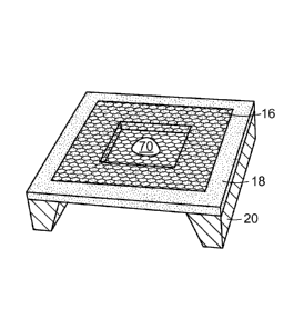
100611 Fig. 5A schematically presents an example of the resulting
nanopore 70 produced in a nanometric material 16 that is self-supported and
that extends across an opening in a frame 18 on a substrate 20. Fig. 5B
CA 02829833 2013-09-10
WO 2012/125770 PCT/US2012/029132
similarly schematically presents an example of an array of nanopores 75
produced simultaneously in a self-supported nanometric material 24, on a
frame 28 and substrate 29 with distinct selected regions of nanometric
material 76 in which nanopores are provided in a controllable fashion.
5 [0062] An ion beam, electron beam, or other suitable beam of
energy
that can be directed to the plane of a nanometric material can be employed in
this nanopore formation step. For many applications, a low-energy ion beam
that is unfocused on the scale of the nanopore can be preferred, given the
production of nanopore nucleation sites also by an ion beam. An all-ion beam
10 process enables large-scale production in an efficient, practical
manner, with
the entire process conducted in a single inexpensive apparatus in which large
device areas and/or many devices can be processed in parallel.
[0063] Because the beam is employed in the nanopore formation step to
selectively remove atoms only from the edge of the nanopore nucleation site,
15 the energy of the incident beam is tuned specifically to this condition.
Particles of the beam therefore preferably are characterized by an energy that
is greater than that required to remove an atom at the edge of the nanopore
but less than that which would remove a bulk atom from the interior of the
material. To quantify this condition, there can be defined an edge atom
20 displacement energy, Ededge, given as the energy required to remove an
atom
from the edge of a nanometric material. An incident particle beam should
have an energy such that the maximum transmitted energy, Trn, in a single
scattering event, as expressed in Expression (1) above, is set as:
gidge < Trn, <E'
(4)
[0064] The value of Ededge, if unknown, can be estimated by summing the
bonding energies for an atom at an edge of the lattice of the nanometric
material, using, e.g., tabulated values. Considering, e.g., a graphene edge
atom, which on average has two bonds to the bulk lattice, then Ededge 6.4 eV
CA 02829833 2013-09-10
WO 2012/125770
PCT/US2012/029132
21
x 2 = 13 eV, a value that is reasonably close to the experimentally-measured
value of 14.1 eV. Based on this value, if there is employed an energetic beam
having an energy such that Tin -= (Edbulk Ededge)I2 = (19 13)/2 = 16 eV,
then
only the atoms at the edge of a nanopore nucleation site in graphene will be
removed. This value can be further tuned empirically to optimize the removal
of atoms at the edge of a nanopore nucleation site without creating additional
defects in the bulk lattice.
100651 Once one has selected an appropriate energy for the beam then
the rate of edge atom removal can be measured, either during irradiation if a
detector is available in situ to detect the particles transmitted through the
membrane or on several samples with stepwise increases in dose followed by
imaging to determine the number of atoms removed per incident particle dose.
The irradiation of a nanopore nucleation site by the energetic beam is
continued until a sufficient beam particle dose has removed a sufficient
number of edge atoms at the nanopore nucleation site to form a nanopore of
selected size. For example, given the use of an 80 keV electron beam to form
nanopores at nanopore nucleation sites in graphene, then an electron beam
fluence of about 3 x 10³ e-/A2/s, can form a nanopore having a 20 A radius in
about two hours. Thus, the energetic beam dose can be a priori selected to
produce a corresponding nanopore size.
100661 As an alternative to dry beam processing, if it is desirable to
maintain a nanometric material in a liquid solution, a selected solution can
be
employed to preferentially react with nanopore nucleation sites on the
nanometric material. For example, given a graphene material, then nitric
acid or other solution chemistries that are known to preferentially react with
disturbed nanometric sites, such as non-six-membered carbon ring lattice
structures, or the edges of a graphene lattice, can be employed to form a
nanopore at a nanopore nucleation site in the graphene. Continued chemical
exposure with, for example, nitric acid, can effect controlled removal of
atoms
CA 02829833 2013-09-10
WO 2012/125770 PCT/US2012/029132
22
from only the disturbed site and the subsequently-formed nanopore edge,
while leaving the rest of the undisturbed graphene intact. Such chemical
treatment can be preferred for feed-back control of the nanopore size by
monitoring ionic flow through the growing nanopore in the sheet of graphene.
.. Once a nanopore of selected size has been produced, the reaction can be
terminated by, e.g., introduction of a neutralizing base species, such as KOH,
into the solution, or provision of another basic solution. Alternatively, an
automatically operative set of solutions can be employed, e.g., with an acid
on
one side of the nanometric material, to etch a nanopore in the material, and a
basic solution on the other side of the nanometric material to neutralize the
acid and stop the nanopore formation process. The ratio of acid molarity to
basic molarity can here be specified to determine the nanopore size at which
etching ceases.
100671 It is found that like nanopore nucleation site formation,
nanopore
formation itself can be influenced by temperature. For example, during
irradiation at room temperature, atoms can diffuse around the inside edge of
the nanopore, affecting the overall nanopore shape. Controlling the
temperature of the nanometric material during irradiation can therefore be
preferred to enable an ability to increase or decrease the amount of material
diffusion that occurs at the evolving nanopore edge, and thus control the
shape of the nanopore. For many applications, a nanopore formation
temperature of between about 78 K and less than about 300 K or less than
about 200 K, can be preferable.
100681 The shape of an evolving nanopore can also be controlled by
using
a focused electron beam, such as that in a scanning transmission electron
microscope (STEM), and slowly moving the focused beam area to etch away
only particular portions of the edge of the nanopore. The nanopore shape can
also be modified by exposing the nanometric material to an increased
CA 02829833 2013-09-10
WO 2012/125770 PCT/US2012/029132
23
temperature after irradiation to adjust the shape, e.g., roundness, or other
aspect of the nanopore.
100691 For many applications, it can be preferable to empirically
characterize the nanopore formation process so that a nanopore diameter
specified a priori can be produced with a corresponding beam dose. In one
method for determining such, there is experimentally determined the
nanopore size that results as a function of total dose, e.g., total electron
dose.
For example, for the nanometric material graphene, the edge of graphene is
characterized by a distinct defocused fringe pattern in a transmission
electron
micrograph (TEM). The radius of a nanopore in a graphene region can be
determined by selecting the center of the nanopore and integrating the image
intensity over azimuthal angles as a function of radius, dividing by the
circumference at that radius as a normalization. The point of inflection of
the
defocused edge fringe can be identified as the average radius of the nanopore.
100701 For many applications, it can be convenient to image the
nanopore during its formation to obtain the requisite radius data. For
example, given nanopore formation in graphene, TEM exposure to a de-
focused electron beam at an energy of about 80 keV enables formation of a
nanopore at a nanopore nucleation site and provides imaging capabilities for
real-time imaging of the nanopore evolution. Similarly, the nitric acid-based
nanopore formation process described above enables feedback control provided
by the monitoring of ionic current flow through an evolving nanopore.
100711 However nanopore radius data is collected, once such is
available,
there can be determined the correlation between dose and nanopore radius for
given nanometric material and beam irradiation conditions and temperature,
such that an essentially automated approach to formation of a nanopore of
prespecified diameter can be enabled. The circumference of a nanopore can be
specified as increasing linearly with dose as nanopore edge atoms are removed.
For a circular nanopore, this can be specified for the nanopore radius, r, as
r =
CA 02829833 2013-09-10
WO 2012/125770 PCT/US2012/029132
24
Md where d is the dose, e.g., in electrons/unit area, and where M is the
measured constant of proportionality.
100721 With this specification for obtaining a selected radius, there
is
enabled the ability to form large populations of monodisperse nanopores in a
selected nanometric material. Such nanopore populations can be particularly
important for, e.g., microfluidic applications such as filtering, molecular
analysis, and chemical reactions. In general, to enable such applications, the
nanometric material is impermeable to a species that is intended to be passed
through the nanopores. The nanopores can be formed in an array that is
ordered or in a random configuration, and that is monodisperse in diameter.
The term monodisperse is herein meant to refer to a monodispersity in
diameter of a plurality of nanopores in a population of nanopores, with a
variation of about 30%. This monodispersity can be achieved in a nanometric
material with the two-step nanopore formation method to produce, e.g., a
plurality of nanopores each having a diameter of, e.g., no greater than about
10 nm, e.g., no greater than about 4 nm, in a population of, e.g., about 1000
nanopores/cm2 having a monodispersity in diameter with a variation of about
30%. In a further example, this monodispersity can be achieved in a
nanometric material for a selected number of nanopores, e.g., at least about
50
nanopores, each having a diameter of, e.g., no greater than about 10 nm, e.g.,
no greater than about 4 nm, having a monodispersity in nanopore diameter
with a variation of about 30%.
100731 This nanopore formation control can be easily exploited to
repeatedly and reliably form populations of nanopores that meet specific
requirements for a range of applications. Whether one nanopore, a small
plurality of nanopores, or a large population of nanopores is needed, the two
step nanopore formation process enables atomic-scale control of the nanopore
formation process.
CA 02829833 2013-09-10
WO 2012/125770
PCT/US2012/029132
Example 1
Formation of a 20 A nanopore in graphene
100741 The nanometric material graphene was synthesized by chemical
vapor deposition on a 25 jam-thick polycrystalline copper substrate (Aesar).
5 The substrate was annealed at low pressure under continuous H2 flow at
1000
C for ¨10 minutes, exposed to an additional flow of CH4 for ¨10 min at 1000
"C to grow the graphene, and then allowed to cool back to room temperature
under continuous gas flow, requiring about 2 hours. After growth, the
graphene was transferred to gold TEM grids covered in a thin amorphous
10 .. carbon film with regular arrays of micron scale holes (Quantifoil, Au
1.2/2.0).
A drop of deionized water was placed on the TEM grid and then the grid was
placed on the graphene, which was pulled into contact with the graphene by
the receding interface from the water droplet. The copper was then etched
away from below by floating the structure on top of FeCl3 copper etchant
15 (Transene). Once etched, the sample was then floated in 1N HC1 to remove
residual iron from the FeCl3 and then floated in three rinses of deionized
water to remove any residual salt, and dried in dry nitrogen.
100751 At this point, several of the structures still contained
variable
amounts of surface contamination that likely formed during the growth
20 procedure, so bake-out of the contamination was conducted. The TEM grids
were transferred to a stainless steel UHV chamber that was just baked to 400
C, evacuated to <10-8 torr, and then baked overnight at 300 C. The final
pressure in the chamber after bake-out was ¨5 x 10⁻⁹ torr. The structures
were then stored in this chamber under UHV at room temperature until use.
25 100761 To produce isolated nanopore nucleation sites in the
graphene
lattice, the structures were transferred to an ion sputtering system capable
of
irradiating samples at various temperatures with a known dose of ions under
UHV conditions. The beam fluence was calibrated by measuring the count
rate of the beam limited by an aperture of known size. Each structure was
CA 02829833 2013-09-10
WO 2012/125770 PCT/US2012/029132
26
inserted through a load-lock mechanism and then cooled to the base
temperature of 148 K. The residual pressure in the chamber was <10-9 torr,
and the residual partial pressures of species up to 100 AMU were monitored
with an in situ residual gas analyzer (Ametek) to ensure that there were no
detectable hydrocarbons, water, or other reactive species in the chamber
during irradiation.
100771 To produce nanopore nucleation sites in the graphene, the
positive argon ion beam was pulsed with a duty cycle of 500 msec on-500 msec
off until the structure reached the desired dose that was computed to produce
the requisite disruption to the graphene, here 1 x 10¹³ Ar+/cm2 at 3 keV. .
The
sample was cooled to 149 K to reduce the probability of diffusion of atoms on
the surface of the graphene, thus preventing atom movement from
immediately repairing newly-formed nanopore nucleation sites in the lattice.
Theoretically, each ion that transits the graphene has the ability to remove
one or two atoms from the lattice, and the sputter yield for an argon ion at 3
keV on graphene is estimated to be of the order 0.5 carbon atoms removed per
incident argon ion. After ion beam exposure to form nanopore nucleation sites
was complete, the structure was then warmed back to 300 K and transferred
to a small UHV chamber for storage.
100781 The structure was then transferred to a transmission electron
microscope (TEM) for controllably producing a nanopore. With the TEM, a
single crystalline grain of graphene was identified using selected area
diffraction, and the grain was verified as single-layer from relative
diffraction
peak intensities at 0 tilt. A selected region in the grain at which an ion-
beam
induced nanopore nucleation site existed was then continuously irradiated by
a parallel, 80 keV electron beam, and images of the process were acquired at
or 60 second time intervals. The nanometric material structure was
nominally maintained at room temperature within the electron microscope.
The irradiation was periodically stopped as the nanopore diameter grew, to
CA 02829833 2013-09-10
WO 2012/125770
PCT/US2012/029132
27
verify the control of the process. At an electron beam fluence of 3 x 10³ e-
/A2/s,
it was found that a nanopore of 20 A radius was formed in about two hours.
100791 Before and after the electron beam irradiation, the electron
beam
current was measured with a Faraday cup integral to the structure holder
(Gatan single-tilt holder), attached to a pico-ammeter (Keithley 2400), and
the
beam area was measured directly from an image of the graphene grain
irradiation area, which was limited by the condenser aperture. The largest
contribution to systemic error is likely the beam current measurement, due to
backscattering and secondary electron loss out of the 0.49 steradians of exit
angle subtended by the entrance to the Faraday cup.
100801 All other systematic biases were estimated to contribute <1%
error to cross section measurements. Residual pressure was less than 1.3
10-7 torr, and a liquid nitrogen anti-contamination device in close proximity
to
the structure protected it from contamination and residual water vapor in the
column during electron irradiation. Objective lens aberrations were corrected
to 3rd order using a post objective hexapole corrector (CEOS), aligned to have
Ci +300 A, C3 -1 pm, and all other aberration coefficients minimized.
Images were zero-loss filtered to ¨1 eV about the primary energy of 80 keV
using the in-column omega filter to improve high-resolution phase contrast by
removing the inelastic electrons. Micrographs were collected on a Gatan
Ultrascan 4k camera or a TIVPS 4k camera at a nominal instrument
magnification of 400-800 kX or camera length of 450 mm for selected area
diffraction.
Example 2
Characterization of graphene nanopore radius correlation to dose
100811 To quantify the correlation between the radius of a nanopore in
graphene as a function of dose of electrons employed to produce that nanopore
radius, the two-step nanopore formation process of Example 1 was conducted,
here with an ion beam dose of 1 x 10¹³ Ar /cm2 for producing nanopore
CA 02829833 2013-09-10
WO 2012/125770 PCT/US2012/029132
28
nucleation sites in the graphene, and with an electron fluence of 3190 50 e-
/A2/s for producing a nanopore at the sites. Sequential micrograph images
containing multiple growing pores were obtained and analyzed by integrating
the micrograph intensity over azimuthal angles as a function of radius,
dividing by the circumference at that radius. The point of inflection of
defocus
at edge fringe was identified as the average radius of the nanopore.
100821 Micrographs were drift corrected using a cross correlation
algorithm and post-processed in ImageJ, with a low-pass filter to a 1.0 A
cutoff, adjusted to 8 bits of linear contrast about the mean intensity value,
and
cropped to the region of interest. The total exposure time in a particular
micrograph was then determined by subtracting the image time stamp from
the exposure start time. The exposure time multiplied by the beam fluence
was then taken as the dose for a particular micrograph, as the beam current
varied by <2% during the course of the experiment.
100831 Fig. 6A is a plot of the resulting data for nanopore radius as a
function of electron dose, where each data point is derived from the azimuthal
integral of a nanopore image in a sequence of acquired images. Analysis on
four additional nanopores produced under the same conditions resulted in
measurement of random error in the slope of radius versus dose, and is
identified by the grey region. The black line is a best linear fit to the
trajectories for the total of five nanopores analyzed. Fig. 6B is a plot of
each of
the five sets of nanopore radius data, here provided separately.
100841 Based on this experimental data, it is found that the
circumference of the nanopore increased linearly with dose as nanopore edge
.. atoms were removed. The average total cross section, o-e, for removing the
nanopore edge atoms was determined from the experimental data, based on
the slope and the density of carbon atoms at the nanopore edge. The result is
8.9 0.4 x 10⁻²⁴ cm2, where the error is the standard deviation from 5
measurements. Using conservative estimates of the systematic error in the
CA 02829833 2013-09-10
WO 2012/125770 PCT/US2012/029132
29
measurement technique, the upper and lower bounds on this value are 9.4 and
7.5 >< 10-24 cm2 respectively.
Example 3
High-density nanopore formation in graphene
100851 Following the process of Example 1, a graphene region of 6.27 x
105 A2 was exposed first to a 3 keV beam of argon ions to impose a dose of 1 X
1013 Ar+/cm2 in the formation of nanopore nucleation sites, and then exposed
to an electron beam to impose a dose of 9.7 x 10⁶ e-/A2 to form nanopores at
the
nucleation sites. Fig. 7 is a micrograph of the resulting structure,
identifying
32 nanopores, as indicated by arrowheads. The locations of some of the
smaller and larger nanopores in the image were determined by looking at
preceding and subsequent images in a series of images. The resulting
nanopore density corresponds to 5.1 x 10¹¹ nanopores/cm2. This correlates
with the ion beam dose of 1 x 10¹³ Ar /cm2 as each 3 keV Ar+ having a
probability of about 5% of nucleating a nanopore under these irradiation
conditions.
100861 Fig. 8 is a plot of nanopore radius distribution for the
nanopores
shown in the image of Fig. 7. The nanopore radius distribution is found to be
sharply peaked. This data demonstrates that the nanopore formation process
is particularly effective at producing monodisperse nanopores. Monodisperse
is here defined as a distribution in radius of 30%.
Example 4
Comparative example of electron beam irradiation
without nanopore nucleation site production
100871 An experiment was conducted to confirm that nanopore
nucleation site synthesis is required to enable nanopore formation in
accordance with the method described above. In the control experiment, a
graphene region of 6.27 x 10⁶ A2 was prepared in the manner of Example 1,
corresponding to the graphene region extent of Example 3. The synthesized
graphene was exposed to an 80 keV electron beam to impose an electron dose
CA 02829833 2013-09-10
WO 2012/125770 PCT/US2012/029132
of 9.7 x 10⁶ e-/A2 in the manner of Example 3. This electron beam energy
meets the requirement of the two-step nanopore formation method in that 80
keV is lower than the required to remove bulk graphene atoms, in the interior
region of the graphene material. No ion beam irradiation step to first form
5 nanopore nucleation sites was conducted. After the electron beam dose was
produced, the graphene was examined, and was found to include no
nanopores. This confirms that without the formation of nanopore nucleation
sites, the electron beam dose does not form nanopores.
100881 This description and examples demonstrate that the nanopore
10 nucleation and formation process provides an elegantly uncomplicated,
efficient, and repeatable process that can be implemented on a large scale
over
large areas and many devices. Many applications requiring mass-production
of nanopores can therefore be implemented in a practical manner and
reasonable cost.
15 100891 It is recognized, of course, that those skilled in the
art may make
various modifications and additions to the processes of the invention without
departing from the spirit and scope of the present contribution to the art.
Accordingly, it is to be understood that the protection sought to be afforded
hereby should be deemed to extend to the subject matter of the claims and all
20 .. equivalents thereof fairly within the scope of the invention.
100901 We claim: