Note: Descriptions are shown in the official language in which they were submitted.
MICROFLUIDIC SYSTEM HAVING MONOLITHIC NANOPLASMON IC STRUCTURES
Field of the Invention
The present invention is related to microfluidic systems and devices having
nanoplasmonic features, particularly for use in cell culture applications, and
to processes
of producing such systems and devices.
Background of the Invention
Analysis of molecular binding and cell behavior are important for disease
diagnostics, biomedical research, and drug discovery. The vast majority of
array-based
studies of bioaffinity interactions employ fluorescently labeled biomolecules
or enzyme-
.. linked colorimetric assays. However, there is a need for methods that
detect bioaffinity
interactions without molecular labels, especially for biomolecular and
cellular interactions,
where labeling is problematic and can interfere with their biological
properties. The
development of simple and specific biosensors to detect biomarkers and measure
cellular
response has far-reaching implications in their timely detection which is of
great concern
to human health and safety.
The advances in genonnics and proteomics have unveiled an exhaustive
catalogue of biomarkers that can potentially be used as diagnostic and
prognostic
indicators of genetic and infectious diseases. The antibody and nucleic acid
fluorescence-
based detection approaches currently consist of complex, multi-step, time
consuming,
and labor intensive assay formats and target analyte analysis to ensure the
specificity of
detection. Additionally, these methods are not suitable for the rapid pathogen
or cancer
detection as they require extensive blood culture of the pathogen or diseased
tissue in
the central laboratory prior to the detection of antibodies.
The analysis of bio-molecular interactions is also a key part of the drug
discovery
process which involves determining the binding affinity of the drug to the
target protein of
interest. Even though developments in the field of high-throughput screening
(HIS) and
computational chemistry greatly accelerated and facilitated the drug finding
process,
there are significant limitations to overcome. An example is the fluorescence-
based HTS
1
CA 2830103 2018-08-10
CA 02830103 2013-09-13
WO 2012/122628
PCT/CA2012/000203
assay, which may generate false positive (e.g. binding to the reporter enzyme
or direct
hydrophobic interaction of the label with the target) or false negative
results (e.g.
occluding of the binding site). The application of novel and efficient label-
free
technologies is of high importance to the drug discovery process, since they
will lower
development costs and decrease the time to market.
For drug discovery as well as in the biomedical research, the study of the
effect of
the specific cues (e.g. chemical, topographical, flow, etc.) on cell
attachment and motility,
cell viability, cell proliferation and cell cycle is of paramount importance.
Inducing and
subsequent measurement of a specific cellular response requires providing the
cells with
the appropriate cues, to control the conditions in the cell microenvironment,
and to
monitor cellular responses on multiple hierarchical levels within a large
number of parallel
experiments. Currently employed assays that rely on cell culture in Petri
dishes and
subsequent fluorescence-based live-cell imaging and biomolecule detection are
slow,
cumbersome and cannot meet these requirements. Multi-well plate assays can
increase
the throughput through automatic imaging afforded by high content cell
screening
(HCCS). However, an important consideration for the multi-well assays is
ensuring
uniform patterning or treatment of each well which is often precluded by
variations in the
volume of liquid dispensed into each well. The resulting variability in the
concentration of
applied reagents hinders fair and quantitative comparisons and limits the
ability of HCCS
to resolve small differences in cell signaling responses. This issue is
exacerbated in more
complex protocols, such as sequential exposure of cells to different media,
because of
errors that accumulate when changing media. Moreover repeated media
aspirations
might unintentionally remove cells from the wells. Because these assays are
also difficult
to miniaturize, HCCS experiments may consume large quantities of expensive or
valuable
cells and reagents. Finally HCCS still relies on fluorescent tags which may
trigger
unwanted steric hindrance effects.
Consequently, the research into the effect of cues (single or multiple) on
cellular
response to date has been limited by the lack of robust and reproducible
methods for
homogeneous material production, precise control of the cell culture
conditions and in situ
real-time label-free monitoring of cellular response, cell behavior, cell
viability or
biomolecular binding interactions. Specifically, the material production
methods have
lacked the control required to reproducibly fabricate homogeneous surfaces
that will allow
investigations into specific interactions between cells and isolated variables
i.e. a
precisely defined nanoscale patterns in a defined space with control over the
induced
change in topography and associated changes to surface energy. The commonly
2
CA 02830103 2013-09-13
WO 2012/122628 PCT/CA2012/000203
employed well-based cell culture methods are costly and suffer errors in
liquid
dispensing, both manually and robotically, thus precluding uniform handling of
each well
which in turn limits how finely signaling responses may be resolved. Finally,
while the use
of fluorescent imaging techniques for cell analysis can provide information
not easily
attainable by other methods, they are usually confounded by the need to over-
express
the signaling protein of interest and by possible effects of the fluorescent
marker on the
protein's function. Therefore due to the phenomenological nature of current
studies, the
responses achieved have been heterogeneous at both single cell and cell
population
levels (Balasundaram 2007; Barbucci 2003; Blummel 2007; Curtis 2006; Dalby
2007a;
Ernsting 2007; Kimura 2007; Salber 2007).
Fluorescence and chemiluminescent detection are the most common methods
employed for biomolecule recognition. Both schemes require the use of a
labeled
recognition element which binds to a molecule of interest thus producing a
selective
signal upon binding (Marquette 2006). Currently, the detection and
quantification of
genomic and proteomic biomarkers from serum or other physiological samples
rely on
solid-phase detection, where strong amplification chemistry is often needed to
produce a
readout. In the case of DNA markers, the state of the art relies on polymerase
chain
reaction (PCR), while for the protein markers enzyme-linked immunosorbent
assay
(ELISA) prevails. Many attempts at miniaturizing bench-top systems using
microfluidics in
order to increase the detection limits and reduce incubation times, reagent
consumption
and sample size have been reported with impressive results (Zhang 2009a; Zhang
2009b; Lim 2007; Lee 2006; Malic 2007). However, despite a growing focus from
the
microfluidic research community, both PCR and ELISA rely on fluorescence
labels, which
increase the complexity and cost of the assay. In addition to the requirement
for a labeled
recognition element, these techniques typically require complex optical
systems which
typically consist of a large microscope or a microplate reader. As a result,
the field of
microfluidics has yet to produce many commercial devices for disease
diagnostics (Myers
2008). There is a need for coupling and integrating microfluidics with direct
label-free
detection methods that base themselves on physical characteristics of biologic
phenomena and have the potential to reduce reagent costs and test complexity
(Weigl
2008).
The development of minimally invasive techniques to induce a specific cellular
response is focused on controlling the direct contact and interaction between
a given cell
type and a well defined material. One way of controlling cell adhesion and
subsequent
morphology is by nanotopography. Research has shown that cells can detect and
3
CA 02830103 2013-09-13
WO 2012/122628 PCT/CA2012/000203
respond to an array of topographies and can be affected by the level of order
of an
induced topography, with clear effects on cell functionality (Dalby 2009;
Dalby 2008;
Dalby 2007b; Dalby 2007c; Dalby 2007d; Hochbaum 2010). Similarly, bacteria
also
respond to topographical (spatial and mechanical) cues and spontaneous
bacteria
patterning on a periodic nanostructure array has recently been shown (Hochbaum
2010).
Another method employs chemically modified surface to induce cellular response
(Cavalcanti-Adam 2008). For both strategies to prove successful the material
must be
homogenous, robust and fabricated or functionalized in a reproducible manner.
To date,
several methods have been used for this purpose, including electron-beam
lithography,
nanoimprint lithography and dip-pen nanolithography (Cavalcanti-Adam 2007;
Curran
2010). However, the assays in these studies were performed using traditional
cell-culture
methods and analyzed using live fluorescence microscopy with inherent
drawbacks of
these techniques which may have resulted in misleading interpretation of
results due to
error in liquid handling, perturbation caused by fluorescent markers and low
throughput in
which only a few cells were imaged for each experimental run.
Flow cytometry (FC) and laser scanning cytometry (LSC) are the most widely
used techniques for cell analysis with well characterized distributions of
cellular
behaviour. Both techniques use fluorescent dyes to label biomolecules of
interest within
the cell in order to reveal the information about the quantity of biomolecules
within the
cell. Flow cytometry involves the hydrodynamic isolation of individual cells
thus affording
high throughput serial analysis. However, FC is limited to characterizing
fluorescent
signals (GFP-fusion proteins, immunofluorescence, and fluorogenic substrates
to
intracellular enzymes) (Fayet 1991; Nolan 1998; Krutzik 2006), which can lead
to steric
hindrance and is incapable of important time-dependent measurements of the
cell
population. Conversely, laser scanning cytometry (LSC) relies on the use of a
scanning
laser to excite the dyes on surface immobilized cells (Griffin 2003; Bedner
1993) thereby
allowing kinetic measurement of time-dependent information in individual
cells. However,
only a limited region of a plate can be scanned thus limiting the throughput
of the
technique. Additionally, the introduction of reagents is performed using a
pipette and only
slow time dependent changes after solution exchange are meaningful. This is
particularly
due to uneven introduction of solution over the whole slide or plate, and the
serial process
of laser scanning. Furthermore, cells analyzed using both methods are usually
grown in
traditional flasks, slides or Petri-dishes before analysis, and so uniformity
of environment
is limited to that of the flask or dish. Notably, cell-cell contact is not
controllable, and
diffusible secretions are maintained in the culture environment.
4
CA 02830103 2013-09-13
WO 2012/122628
PCT/CA2012/000203
To overcome some of these limitations, research has recently shifted towards
the
exploitation of the precise chemical delivery capabilities of microfluidic
devices. The
single most popular approach for the fabrication of microfluidic devices for
cell-based
assays is based on the soft-lithography of polydimethylsiloxane (PDMS). PDMS
is an
elastomer which is casted over a mold typically fabricated using
photolithography and
cured for several hours resulting in a transfer of features from the mold to
the PDMS. Its
wide use as a material of choice is due to its mechanical property, which is
amenable to
integration of fluidic valves, essential elements for major microfluidic
applications. PDMS
platforms for cell culture have been reported in the past especially for two-
dimensional
morphological cells, such as epithelial cells, and several designs have been
the subject of
patent applications (Jin 2010; Lee 2010). However, most of these studies
coupled
microfluidic device to traditional macroscale equipment (i.e. fluorescence
microscopes)
and relied on the use of fluorescence imaging for cellular response analysis.
Moreover, there is surprisingly little work reported on the combination of
nanopatterned surfaces and microfluidics, especially in a way advantageous for
studying
topographically induced cellular response. This is in part due to the
difficulty in
reproducibly fabricating nanostructured surfaces within microfluidic cell
culture devices.
Several production processes have been reported for nanostructure fabrication
inside
microchannels including vapor deposition of nanoparticles (Song 2009), in situ
formation
of nanoparticles inside the channels from catalytic reaction (Fonverne 2009),
and
polymerization of a polymer around an anodic aluminum oxide template (Soper
2008).
However, controlling the regularity, geometry and/or spacing of the
nanoparticle arrays
using these techniques is difficult to achieve limiting the reproducibility of
the
experimental measurements.
In order to obtain spatially controlled geometry and spacing of the
nanostructures
within a PDMS microfluidic channel, multilayer mold comprising nano- and micro-
structures are required with fabrication procedures involving sequential
electron-beam
lithography, interference lithography or nanoinnprint lithography in concert
with
photolithography of SU-8 resist. The compatibility of materials and reagents
involved in
these processes is difficult to achieve. Additionally, once the mold is
fabricated and the
microchannels have been defined, the slightest change of the microfluidic
layout would
require the repetition of complete fabrication process, starting with the
nanostructured
substrate. This can result in topographical surface variations induced by
sample-to-
sample fabrication differences. Furthermore, PDMS soft-lithography fabrication
technique
itself is not well suited for mass production of microfluidic devices which
hinders their
5
CA 02830103 2013-09-13
WO 2012/122628
PCT/CA2012/000203
application in industry, including medical diagnosis and pharmaceutics.
Finally, the use of
PDMS as a material for in vitro models for cell culture needs to be considered
in a
biological context due to the leaching of uncured oligomers from the polymer
network into
microsystem media (Regehr 2009).
Further, microfluidic devices with nanostructured hydrophobic surfaces have
been
developed to control surface tension and liquid pressure in fluid flow
channels (Extrand
2005), but the standard techniques used to nano-pattern the channel surfaces
are
insufficiently flexible to permit simple and fast patterning of
nanostructures, especially
different nanostructured patterns, at specific locations in the channels or
chambers of the
device but not at others. Thus, different design features within the same
device are
difficult to accomplish and the designs are difficult to adapt to the
requirements of
plasmonic detection techniques.
In general, prior art systems have one or more deficiencies. There is a lack
of an
integrated microfluidic system that relies on non-invasive, label-free
detection
technologies including plasmonic techniques such as surface plasmon resonance
(SPR)
(e.g. reflection-mode SPR, transmission-mode SPR, localized surface plasmon
resonance (LSPR)) and surface-enhanced Raman spectroscopy (SERS) for
monitoring
cell behavior, cell-substrate interactions, cell response to stimuli and
biomolecule
detection. There is a lack of fabrication techniques allowing monolithically
integrated
nanostructured cell culture system in long-term biocompatible materials with
simultaneous cell guiding functionality and plasmonic detection capability
using
topographical cues and nanostructure plasmonic response, respectively. There
is poor
control of cellular microenvironment in Petri-dish or microwell plates. There
is lack of
reproducible and robust surface topography (nanopatterning) for precise
control of
cellular response and cell-substrate interaction studies. There is a lack of
integrated
nanostructured surface within microfluidic channels. And, there is a lack of
low-cost and
rapid mold fabrication techniques that allow interchangeable nano- and micro-
structure
design.
There remains a need for an integrated system that can meet one or more of the
following requirements: (i) efficient control of initial cell adhesion; (ii)
efficient control of the
cellular response to the specific stimulus over a prolonged period; (iii) in
situ, label-free
and real-time monitoring of cellular response, cell mobility, cell behavior,
cell-viability or
biomolecule detection in order to avoid false response due to cellular
secretion of the
molecules to which they respond and steric hindrance induced by the
fluorescent tags.
Additionally, the system is ideally low-cost, portable and amenable to mass-
production.
6
CA 02830103 2013-09-13
WO 2012/122628
PCT/CA2012/000203
Summary of the Invention
In one aspect of the present invention, there is provided a process of
producing a
patterned polymeric substrate comprising: etching one or more ordered patterns
onto a
hard substrate, the ordered patterns comprising ordered arrays of nano-scale
elements
having cross-sectional dimensions in a range of from 10 nm to 1000 nm, the
arrays
having a spacing distance between their respective elements where cross-
sectional
dimension to spacing distance ratio is greater than 0.2; micro-patterning a
polymeric film
to form a membrane comprising a first surface bearing a pattern of micro-scale
and/or
meso-scale features for defining one or more channels and/or chambers, one or
more of
the micro-scale and/or meso-scale features comprising through-holes; placing
the
membrane on the hard substrate with a surface opposite the first surface
against the hard
substrate, the through-holes aligned to expose the one or more ordered
patterns, and
applying pressure sufficient to seal lips of the membrane surrounding the
through-holes
against the hard substrate; placing a settable liquid polymer or metal in the
through-holes
and over the first surface and setting the settable liquid polymer or metal to
form a stamp
from the settable liquid polymer or metal, the stamp comprising micro-scale
and/or meso-
scale reliefs for defining one or more channels and/or microfluidic chambers
and further
comprising one or more nano-scale relief patterns on the micro-scale and/or
meso-scale
reliefs that complement the one or more ordered patterns; and, patterning a
polymeric
substrate by stamping the polymeric substrate with the stamp to form the one
or more
channels and/or microfluidic chambers in the polymeric substrate, the
polymeric substrate
comprising one or more surfaces having one or more ordered patterns that are
substantially identical to the one or more ordered patterns etched onto the
hard substrate,
the one or more ordered patterns in the polymeric substrate suitable for
plasnnonic
resonance reading of a fluid within the one or more channels and/or chambers.
In another aspect of the present invention, there is provided a stamp for
patterning
a polymeric substrate, the stamp comprising: a polymer or metal of sufficient
hardness to
be able to pattern the polymeric substrate; and, a pattern of micro-scale
and/or meso-
scale reliefs for forming one or more channels and/or microfluidic chambers,
one or more
of the micro-scale and/or meso-scale reliefs having top surfaces comprising
one or more
nano-scale relief patterns for forming one or more ordered arrays of nano-
scale elements
in the polymeric substrate, the nano-scale elements having cross-sectional
dimensions in
a range of from 10 nm to 1000 nm, the arrays having a spacing distance between
the
elements where cross-sectional dimension to spacing distance ratio is greater
than 0.2.
7
CA 02830103 2013-09-13
WO 2012/122628 PCT/CA2012/000203
In yet another aspect of the present invention, there is provided a
microfluidic
device comprising a monolithic polymeric substrate patterned with one or more
micro-
scale channels in fluid communication with one or more microfluidic chambers,
a surface
in the polymeric substrate comprising an ordered array of nano-scale elements
suitable
for plasmonic resonance reading of a fluid on the surface, the nano-scale
elements
having cross-sectional dimensions in a range of from 10 nm to 1000 nm, the
array having
a spacing distance between the elements where cross-sectional dimension to
spacing
distance ratio is greater than 0.2.
Microfluidic devices of the present invention are monolithic microfluidic
structures
in a polymeric substrate having nanostructures monolithically integrated in
the substrate.
The devices have at least one micro-scale channel in fluid communication with
at least
one microfluidic chamber. Channels include, for example, sample loading
channels, cell
loading channels, medium perfusion channels, mixing channels, particle
separation or
fractionation channels, gradient generating channels and high resistance
perfusion
conduits, which may have different channel dimensions dictated by the specific
application. Microfluidic chambers include, for example, cell culture
chambers, bacteria or
cell capture chambers, biomolecular interaction chambers or mixing chambers.
Other
microfluidic structures may also be present, for example valves and pumps for
controlling
fluid flow, conduits, inlets, outlets, and the like.
At least one surface in a channel or microfluidic chamber of the device is
patterned with an ordered array of nano-scale elements suitable for plasmonic
resonance
reading of a fluid on the surface. More than one surface may be patterned and
the pattern
may be the same or different. The patterned surface or surfaces may be
anywhere in the
device, and could even be everywhere in the device. The location of the
patterned
surface or surfaces is dictated by the ultimate use of the device. Such
patterned surfaces
may be called "nanoplasmonic surfaces", and the elements may be called
"nanoplasmonic elements". The nano-scale elements may serve a dual purpose as
both
nanoplasmonic elements and nano-topographical cues. To function as a
nanoplasmonic
surface, the ordered array of nano-scale elements has a highly regular or
periodic pattern
.. designed to have a specific plasmonic resonance to permit label-free, real-
time optical
reading using plasmonic techniques. The regularity of the pattern is reflected
in very
consistent size, spacing and/or geometry of the nano-scale elements, and
arises from the
highly reproducible process employed in the present invention to produce the
patterned
polymeric substrate of the device. Preferably, for each of the size, spacing
and/or
geometry of the elements in the array, the standard deviation from the
respective average
8
CA 02830103 2013-09-13
WO 2012/122628 PCT/CA2012/000203
is no more than about 3%, preferably no more than about 2.5%, and may be no
more
than about 1%.
The nano-scale elements have cross-sectional dimensions in a range of from
about 10 nm to about 1000 nm, which is in the nano-scale range. Preferably the
cross-
sectional dimensions are in a range of from about 10 nm to about 750 nm.
Individual
nano-scale elements preferably have an aspect ratio (height to width) of about
100 or
less, more preferably 50 or less, yet more preferably 10 or less. Aspect
ratios may be in a
range of from 100:1 to 1:100, 50:1 to 1:50 or 10:1 to 1:10.
Spacing of nano-scale elements in the ordered array is an important factor in
maintaining suitable regularity for plasmonic resonance reading techniques.
Ideal spacing
distance is dependent on the size of the nano-scale elements. For plasmonic
techniques,
cross-sectional dimension to spacing distance ratio is generally greater than
about 0.2.
Preferably, the ratio of cross-sectional dimension to spacing distance is in a
range of from
about 0.2 to about 1.5, or about 0.5 to about 1. The ratio of cross-sectional
dimension to
spacing distance is commonly about 0.5 or about 1.
The nano-scale elements may have any nanostructure geometry suitable for the
reading technique to be used. Suitable geometries include, for example,
nanopillars,
nanoposts, nanodots, nanorods, nanopyramids, nanocrescents, nanodisks,
nanodomes,
nanoholes, nanogratings or nanogrooves. Multiple arrays having different
nanostructure
geometries for different functionalities (e.g. gratings for light-coupling or
nanopillars for
SPR electromagnetic field enhancement) can be integrated within the same
device.
Multiple arrays having different nanostructure geometries can be co-mingled to
occupy
the same surface, or different arrays can be on different surfaces in the
device. Different
arrays can resonate at different wavelengths permitting implementation of a
multiple
frequency interrogation scheme for parallel multichannel detection of
different targets.
Ordered arrays of nano-scale elements may be integrated onto a surface of
micro-
scale features (e.g. micropillars) in the device. In cell culture
applications, this can provide
two levels of topographical cues (spatial and mechanical cues) on the micro-
and nano-
scales for control of cell attachment and motion while retaining plasmonic
detection
capability for studying cell behavior and interactions. Further, micro-optic
features (e.g.
microlenses, blazed gratings, etc.) may be formed into the microfluidic device
for various
purposes, including enhancing light coupling or improving light collection
efficiency,
depending on the particular reading techniques used.
9
CA 02830103 2013-09-13
WO 2012/122628
PCT/CA2012/000203
Nano-scale elements may be further treated to enhance or alter the properties
of
the ordered array. Such treatments may include, for example, metallization of
the nano-
scale elements to increase reflectivity of the array or chemical surface
modification to
permit attachment of biolmolecules. For plasmonic techniques, metallization of
one side
of the nano-scale elements to form single-sided metallic nano-elements is
particularly
preferred. Silver, gold, copper, platinum and palladium are preferred metals
for
metallization, particularly for SERS applications. Metallization may be
accomplished by
any suitable method, for example, evaporation, sputtering or electroplating.
Chemical
surface modification includes modification with specific reactive end-groups,
for example
.. -COOH, -OH, -NH3, -biotin, -silane, etc., to enable subsequent attachment
of antibodies,
oligonucleotides, aptamers or proteins for cell, bacteria or biomolecule
capture.
The polymeric substrate may comprise any polymeric material that is soft
enough
to be stamped by the stamp. Preferably, the polymeric material is suitable for
fabrication
of microfluidic devices. Preferably, the polymeric material comprises a cyclo-
olefin
.. polymer (e.g. ZeonorT"), a thermoplastic polymer (e.g. polyolefins), a
biodegradable
polymer (e.g. starch, poly-lactic acid), an elastomer (e.g. thermoplastic
elastomer (TPE)
or any blend thereof. More preferably, the polymeric material comprises a
cyclo-olefin
polymer (COP) (e.g. ZeonorTM) or a thermoplastic elastomer (TPE).
The stamp may comprise any polymer or metal that is settable from liquid form
to
.. produce a polymer or metal that is harder than the polymeric substrate and
hard enough
to impress the ordered pattern on the polymeric substrate. If a metal is used,
the metal in
its liquid state must not be hot enough to melt the hard substrate and
polymeric film.
Preferably, a settable polymer is used and the polymer is a curable polymer,
preferably a
curable thermoset polymer. The polymer for the stamp may be settable or
curable
thermally, chemically or with light. Photo-curable polymers, especially ones
cured by UV
light, are particularly preferred. Some examples of photcurable polymers
include MD-700
and DarcourTM blend. The stamp is used to transfer all of the features of the
microfluidic
device into the polymeric substrate in one processing step. The processing
step may
involve any suitable method for patterning polymeric substrates using stamp or
dies, for
.. example, hot embossing, nanoimprint lithography or injection moulding. The
stamp may
be treated to facilitate patterning of the substrate, for example, treating
the stamps with a
release agent can facilitate separation of the patterned polymeric substrate
from the
stamp. Since the stamp comprises reliefs for all of the features of the
microfluidic device,
the microfluidic device can be formed completely in one step resulting in a
monolithic
device having all of the features of the device integrated into the polymeric
substrate.
CA 02830103 2013-09-13
WO 2012/122628
PCT/CA2012/000203
Further, the stamp can be re-used to make more devices and the use of the
stamp
provides pattern and dimensional consistency between devices produced in
different
production runs. These are distinct advantages over prior art processes for
producing
microfluidic devices.
The stamp may be fabricated from a master mold by transferring features from
the
master mold to the settable polymer. The master mold comprises a hard
substrate and
one or more membranes placed on the hard substrate. The hard substrate may
comprise
a metal, a silicon wafer, a glass substrate or a hard polymer. The term "hard
substrate"
refers to a substrate that is harder than the membranes placed on the
substrate.
Preferably, the hard substrate comprises a hard polymer, for example, a cyclo-
olefin
polymer (e.g. ZeonorTm), a polymethylmethacrylate (PMMA), a polycarbonate (PC)
or a
polyetheretherketone (PEEK). The one or more membranes comprise polymeric
films of a
soft polymer, for example, polydimethylsiloxane (PDMS), a soft thermoplastic
polymer
(e.g. a soft polyolefin) or a soft thermoplastic elastomer (e.g. KratonTM,
MedipreneTM, CL-
30 or styrene-ethylene-butadiene-styrene (SEBS)). The polymeric films are
preferably
films of soft thermoplastic elastomer (TPE). The term "soft polymer" refers to
a polymer
that is softer than the hard substrate.
One or more ordered patterns comprising nano-scale elements are etched onto
the hard substrate. Etching can be accomplished by any suitable means
appropriate for
the hard substrate. For example, etching may be accomplished with lasers, with
ion
bombardment or with chemical etching, for example reactive ion etching, deep
reactive
ion etching, wet chemical etching, electron beam lithography, nanoimprint
lithography, ion
beam milling, laser ablation or interference lithography. The membranes
comprise
polymeric films having one surface onto which micro-scale and/or meso-scale
features
have been micro-patterned. Patterning of the polymeric films may be
accomplished by
any suitable means, for example, hot embossing, injection moulding,
nanoimprint
lithography or roll-replication. The micro-scale and/or meso-scale features in
the
membranes define one or more microchannels and/or microfluidic chambers that
will
eventually be created in the final microfluidic device. One or more of the
features
patterned in the polymeric film may be through-holes that are aligned to
expose the one
or more ordered patterns on the hard substrate. The through-holes have the
shape of the
microfluidic features (e.g. microchannels, microfluidic chambers,
micropillars, etc.) that
are intended bear the ordered patterns in the final device.
The membranes are placed on the hard substrate so that the surfaces bearing
the
micro-scale features are also exposed. More than one membrane may be stacked
on the
11
CA 02830103 2013-09-13
WO 2012/122628 PCT/CA2012/000203
hard substrate and the through-holes aligned with the ordered patterns to
obtain the
desired microstructural features in the device. Use of stacked membranes is
particularly
useful for forming microstructural features, such as micropillars, having a
top surface
covered with the nano-scale elements. When placing the membranes on the hard
substrate, a seal around the through-holes may be achieved by applying
sufficient
pressure to seal lips of the membrane surrounding the through-holes against
the hard
substrate.
The master mold thus formed may be used to fabricate the stamp by placing the
settable polymer in the through-holes and on the membrane surface onto which
the
micro-scale and/or meso-scale features have been micro-patterned. The settable
polymer
is typically poured or injected in liquid form onto and into the master mold
and then set as
described above. In this manner, the settable polymer is in contact with the
features on
the membrane and the ordered pattern on the hard substrate, so when the
settable
polymer hardens, the micro-scale and/or meso-scale features and the ordered
pattern of
nano-scale elements are transferred to the set polymer. Once the settable
polymer has
hardened, the stamp so fabricated can be demolded and then used to pattern the
polymeric substrate to form the final device. Thus, the master mold is an
exact replica of
the final device, and the stamp is the toll used to transfer the pattern in
the master mold to
the polymeric substrate to produce the final device. It is an advantage of the
present
invention that when a different channel layout needs to be used with the same
ordered
pattern of nano-scale elements, the new master mold can be easily fabricated
by
delanninating the soft membranes from the hard substrate an replacing the
membranes
with membranes having the new layout.
The present invention advantageously provides low-cost monolithic integrated
microfluidic systems with multiplexing capability (e.g. valving, pumping) for
precise control
of cell culture conditions that can simultaneously integrate label-free
enhanced plasmonic
techniques such as surface plasmon resonance (SPR) (e.g. reflection-mode SPR,
transmission-mode SPR, localized surface plasmon resonance (LSPR)) or surface-
enhanced Raman scattering (SERS). The present monolithic integrated polymer-
based
microfluidic system has micro- and nano-structures that provide topographical
cues for
cell attachment and culture for controlling cell behavior while permitting
monitoring of
cellular behavior, motility, attachment, viability, biomolecule interactions
or any
combination thereof using plasmonic detection. The system is fabricated using
a simple,
robust and cost-effective process in a single step.
12
CA 02830103 2013-09-13
WO 2012/122628 PCT/CA2012/000203
The present system is advantageous over both conventional and recently
reported
processes employed for cell culture and monitoring of cell behavior as the
present system
integrates in a single monolithic biocompatible substrate both a
nanostructured surface
required for plasmonic response monitoring and a network of microchannels for
precisely
controlling cellular environment, with additional advantages of low-volume
consumption,
rapid low-cost fabrication of molds with easily interchangeable microfluidic
channel
layouts, amenability to mass production, and in situ label-free real-time
detection of
cellular response, viability, behavior and biomolecular binding using enhanced
SPR
(reflection-mode SPR, transmission-mode SPR, LSPR) or SERS.
The present invention has application to such problems as screening molecular
or
cellular targets, cellular identification, screening single cells for RNA or
protein
expression, monitoring cell response to different stimuli (chemical,
topographical, flow,
etc.), genetic diagnostic screening at the single cell level, or performing
single cell signal
transduction studies.
Further features of the invention will be described or will become apparent in
the
course of the following detailed description.
Brief Description of the Drawings
In order that the invention may be more clearly understood, embodiments
thereof
will now be described in detail by way of example, with reference to the
accompanying
drawings, in which:
Fig. 1 depicts a schematic diagram of a process of the present invention for
producing a monolithic integrated nanoplasmonic microfluidic cell culture
system.
Fig. 2a-d depict cross-section schematics of a nanostructured nanoplasmonic
microfluidic cell culture system, where (a) is a cross-section of a chamber
through a
perfusion channel and perfusion conduit, (b) is a cross-section of a chamber
through a
cell-loading channel, (c) is a cross-section through a chamber showing
integrated
micropillars with nanostructured top surface and (d) is a cross-section
through a chamber
showing an integrated micro-optic element on the bottom side of the flow layer
substrate.
Fig 2e-f depict 3D views of the chamber bottom depicted in Fig. 2a containing
micropillars with nanostructured top surface area used to (e) control cell
attachment/motility and (f) study cell-substrate interactions.
13
CA 02830103 2013-09-13
WO 2012/122628 PCT/CA2012/000203
Fig. 3 depicts SEM micrographs of fabricated structures showing (a) different
possible nanoplasmonic nanostructures including nanoholes, nanopillars,
nanoposts and
nanogratings, (b and c) three-dimensional micro- and nano-structures defined
in a single
substrate using a one step fabrication process of the present invention.
Fig. 4 depicts a schematic of a nanoplasmonic microfluidic cell culture system
with
plasmonic detection capability.
Description of Preferred Embodiments
Example 1: Process for fabricating a monolithic integrated nanoplasmonic
microfluidic cell
culture system
A monolithic integrated nanoplasmonic microfluidic cell culture system of the
present invention may be produced generally as shown in Fig. 1, which
illustrates the
process showing a single cell chamber and none of the channels, conduits,
valves or
other microfluidic features for clarity. A soft thermoplastic elastomer film
is hot-embossed
to form micro-scale and meso-scale features (microchannels, conduits,
chambers, etc.) in
TPE membrane 10 including through-hole 11. This is performed at an applied
pressure
ranging from 5 kN to 15 kN, for 5-30 min, at a temperature in a range of from
100 C to
160 C, depending on the desired features. Hard ZeonorTM substrate 12 is
patterned by
hot-embossing at an applied pressure of 10 kN to 20 kN for 10-30 min at a
temperature
ranging from 140 C to 170 C depending on the specific ZeonorTM grade to form a
regular
array of nano-scale grating elements 13. With the micro-scale and meso-scale
features
facing up, the TPE membrane is placed on the ZeonorTM substrate such that the
through-
hole is aligned with the grating elements. The membrane is then reversibly
bonded to the
ZeonorTM substrate to seal the membrane around the through-hole against the
ZeonorTM
substrate to form master mold 14 at room temperature. Photocurable polymer 15
is
poured into the through-hole and onto the membrane to cover the membrane and
the
micro-scale and meso-scale features thereon. Glass or metal backing plate 16
is placed
over top of the photocurable polymer and the photocurable polymer is then
exposed to
UV radiation 17 to cure the polymer. When a metal backing plate is used, the
assembly is
flipped upside down to UV cure the polymer. After curing, master mold 14 and
glass (or
metal) plate 16 are removed to provide working stamp 18 having reliefs 19
comprising a
reverse image of the micro-scale and nneso-scale features and the regular
array of nano-
scale grating elements. The working stamp is then used to hot-emboss "hard or
soft"
thermoplastic polymer substrate 20 (e.g. ZeonorTM, PMMA or a thermoplastic
elastomer
such as CL-30, MedipreneTM, etc.) to provide, in one step, a monolithic
microfluidic cell
14
CA 02830103 2013-09-13
WO 2012/122628 PCT/CA2012/000203
culture system having micro-scale and meso-scale features 21 and regular array
of nano-
scale grating elements 22 therein.
Microfluidic cell culture systems produced in this manner may comprise any
number of cell culture chambers, microchannels, conduits, valves, etc. More
detailed
schematic drawings of one cell culture chamber in the monolithic integrated
nanoplasmonic microfluidic cell culture system produced by this process are
shown in
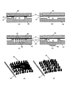
Fig. 2. Referring to Figs. 2a to 2d, flow layer 40 of the cell culture system
comprises cell
loading channels 41, perfusion channels 42, perfusion conduits 43 and culture
chambers
44, which have different dimensions dictated by the specific application. As
shown in
Figs. 2a, 2b and 2d, the bottom of the cell culture chambers may be patterned
with an
ordered array of nanostructures 45, in this case a nanograting. Alternatively,
as shown in
Fig. 2c, the bottom of the cell culture chamber may have integrated
micropillars 46 having
nanostructures 47 patterned thereon. As shown in Figs. 2e to 2f, such
nanostructured
micropillars can provide two-levels of topographical (spatial and mechanical)
cues on the
micro- and nano- scale for controlling attachment/motion (cell isolation or
confinement) of
cells 48, while retaining plasmonic detection capability for the study of cell
behavior and
interactions. Further, as shown in Fig. 2d, flow layer 40 can be fabricated to
include
micro-optic elements, such as microlens 49 of nanograting 45, for enhanced
light
coupling or improved light collection efficiency, depending on the particular
interrogation
scheme (e.g. transmission or reflection SPR, LSPR or SERS).
Control layer 50 and thin membrane 51 may be placed on top of flow layer 40 to
control fluid flow in the channels and conduits of the microfluidic cell
culture system.
Control layer 50 contains a network of channels used to supply pressure on
thin
membrane 51 sandwiched between the control layer and the flow layer in order
to close
the valves and control fluid flow. While for certain application, the use of
valves for fluidic
management might not be necessary, for high-level microfluidic integration of
the system
it is of great importance in order to allow two-dimensional addressing of each
individual
chamber. The monolithic integration of nanostructures with the flow layer
allows the use
of the control layer for the integration of valves which would otherwise be
impossible by
simply assembling a bottom nanostructured SPR layer with a top microfluidic
structure.
Referring to Fig. 3, sample scanning electron microscope (SEM) micrographs of
possible nanostructures and their monolithic integration within microfluidic
chambers of
the microfluidic cell culture system are shown. In Fig. 3a, from left to right
are shown
nanoholes, nanopillars, nanoposts and nanogratings. In each of Figs. 3b and 3c
from left
to right are shown successive magnifications of SEM micrographs of monolithic
three-
CA 02830103 2013-09-13
WO 2012/122628
PCT/CA2012/000203
dimensional microstructures and nanostructures fabricated using the present
method,
where the SEM on the left shows the microstructures, the SEM on the right
shows the
nanostructures in a microstructure and the SEM in the middle has a
magnification in
between the left and right. In 3b and 3c, the SEM in the middle has a
magnification 2.5x
greater than the SEM on the left, and the SEM on the right has a magnification
20x
greater than the SEM in the middle. The field of view for the SEM on the left
is 500 pm.
Example 2: Use of a monolithic integrated nanoplasmonic microfluidic cell
culture system
in plasmonic detection
In operation a monolithic integrated nanoplasmonic microfluidic cell culture
system
of the present invention employs pressure-driven flow to transport cells in
suspension
from a plurality of reservoirs through a plurality of cell-loading channels to
a plurality of
nanostructured cell culture chambers by closing valves of the perfusion
channels and
opening valves on the cell-loading channels. A plurality of cell-lines are
loaded using a
plurality of different reservoirs. Following initial cell attachment on the
bottom of the
nanostructured chambers, the valves on the cell-loading channels are closed,
and fresh
media is continuously injected in each of the perfusion channels. Multiple
high resistance
perfusion conduits ensure equal distribution of the media within the chamber
while
minimizing the shear-stress exerted on the cells.
Once the cell culture chambers are loaded with cells, plasmonic resonance
readings are taken using optical detection methods of Reflection or
Transmission-mode
Surface Plasmon Resonance, Localized Surface Plasmon Resonance or Surface
Enhanced Raman Spectroscopy. Fig. 4 illustrates the configuration of
microfluidic device
60 in relation to light source 62 and detector 64 of the optical detection
method. With
these detection methods, cell-substrate interaction can be monitored in situ,
in real-time
and without any labels by analyzing the shift in the plasmonic peaks of the
nanostructured
substrate response. Resulting shifts in plasmonic peaks for surface plasmon
resonance
(SPR) and localized surface plasmon resonance (LSPR) or surface enhanced Raman
spectroscopy (SERS) are illustrated at the left and right, respectively, in
Fig. 4.
Additionally, the present design allows monitoring of cellular response due to
different bio-chemical cues which can be supplemented in the perfusion media.
Furthermore, prior to cell loading, using the same microchannels, the bottom
of the
chambers can be functionalized by flowing different chemicals and/or
biological species
for monitoring of cell-substrate interactions or for the detection of
biochemical targets
excreted or extracted from the cell.
16
References:
Balasundaram G, Webster TJ. (2007)J. Biomed. Mater. Res., Part A. 80a, 602-
611.
Barbucci R, Pasqui D, Wirsen A, Affrossman S, Curtis A, Tetta C. (2003) J.
Mater. Sci.
14, 721-725.
Bedner et al. (1998) Cytometry. 33, 1-9.
Blümmel J, Perschmann N, Aydin D, Drinjakovic J, Surrey T, Lopez-Garcia M,
Kessler H,
Spatz JP. (2007) Biomaterials. 28, 4739-4747.
Cavalcanti-Adam EA, Volberg T, Micoulet A, Kessler H, Geiger B, Spatz JP.
(2007)
Biophys. J. 92, 2964-2974.
Cavalcanti-Adam EA, Aydin D, Hirschfeld-Warneken VC, Spatz JP. (2008) HFSP J.
2,
276-285.
Curran JM, Stokes R, Irvine E, Graham D, Amro NA, Sanedrin RG, Jamil H, Hunt
JA.
(2010) Lab on a Chip. 10, 1662-1670.
Curtis AS, Dalby MJ, Gadegaard N. (2006) J. R. Soc. Interface. 3, 393-398.
Dalby MJ, Gadegaard N, Tare R, Andar A, Riehle MO, Herzyk P, Wilkinson CD,
Oreffo
RO. (2007a) Nat. Mater. 6, 997-1003.
Dalby MJ, Biggs MJ, Gadegaard N, Kalna G, Wilkinson CD, Curtis AS. (2007b) J.
Cell.
Biochem. 100, 326-338.
Dalby MJ, Gadegaard N, Curtis AS, Oreffo RO. (2007c) Curr. Stem Cell Res.
Ther. 2,
129-138.
Dalby MJ, Gadegaard N, Tare R, Andar A, Riehle MO, Herzyk P, Wilkinson CD,
Oreffo
RO. (2007d) Nat. Mater. 6, 997-1003.
Dalby MJ, Andar A, Nag A, Affrossman S, Tare R, McFarlane S, Oreffo RO. (2008)
J. R.
Soc. Interface. 5, 1055-1065.
Dalby MJ. (2009) Nanomedicine. 4, 247-248.
17
CA 2830103 2018-08-10
CA 02830103 2013-09-13
WO 2012/122628 PCT/CA2012/000203
Ernsting MJ, Labow RS, Santerre JP. (2007) J. Biomed. Mater. Res., Part A.
83a, 759-
769.
Extrand CW, Wright M. (2005) Microfluidic Device with Ultraphobic Surfaces.
United
States patent 6,923,216 issued August 2, 2005.
Fayet al. (1991) Biochemistry. 30, 5066-5075.
Fonverne A, Dijon J, Ricoul F, Rouviere E. (2009) Method of manufacturing a
microfluid
component comprising at least one microchannel filled with nanostructures.
European
patent publication EP 2042467 published April 1, 2009.
Griffin et al. (2003) Febs Letters. 546, 233-236.
Hochbaum A, Aizenberg J. (2010) Nanoletters. D01:10.1021/n11022290k.
Jin Q, Zheng Y, Wu J, Shao J, Zhao J. (2010) Microfluidic cell array chip for
high-
throughput medicament screening, method and use fabricated in PDMS using
modular
SU-8 mold. Chinese patent publication CN 101629143 published January 20, 2010.
Kimura K, Hattori A, Usui Y, Kitazawa K, Naganuma M, Kawamoto K, Teranishi S,
Nomizu M, Nishida T. Invest. Ophthalmol. Visual Sci. 48, 1110-1118.
Krutzik et al. (2006) Nature Methods. 3, 361-368.
Lee LJ, Yang S, Lai S, Bai Y, Huang W, Juang Y, Gregory SM. (2006) Advances in
Clinical Chemistry. (Elsevier) pp. 255-295.
Lee L, Di Carlo D, Tanner N. (2010) Microfluidic Methods for Diagnostics and
Cellular
Analysis. United States patent publication US 2010/003666 published January 7,
2010.
Lim CT, Zhang Y. (2007) Biosensors and Bioelectronics. 22, 1197-1204.
Malic L, Herrmann M, Hoa XD, Tabrizian M. (2007) Recent Patents on
Engineering. 1,
71-88.
Marquette C, Blum L. (2006) Biosensors and Bioelectronics. 21, 1424-1433.
Myers FB, Lee LP. (2008) Lab on a Chip. 8, 2015-2031.
Nolan et al. (1998) Nature Biotechnology. 16, 633-638.
18
CA 02830103 2013-09-13
WO 2012/122628
PCT/CA2012/000203
Regehr KJ, et al. (2009) Lab Chip. 9,2132-2139.
Salber J, Grater S, Harwardt M, Hofmann M, Klee D, Dujic J, Jinghuan H, Ding
J,
Kippenberger S, Bernd A, Groll J, Spatz JP, Moller M. (2007) Small. 3, 1023-
1031.
Song Y. (2009) Preparation process of single nanoparticle and array-based
biological
molecule detector thereof) Chinese patent publication CN 101571536 published
November 4, 2009.
Soper SA, McCarley RL, Chen G, Shadpour H. (2008) Polymeric Nanopillars and
Nanotubes, Their Manufacture and Uses. International patent publication WO
2008/097360 published August 14, 2008.
Weigl B, Domingo G, LaBarre P, Gerlach J. (2008) Lab on a Chip. 8, 1999-2014.
Zhang Y, Ozdemir P. (2009a) Analytica Chimica Acta. 638, 115-125.
Zhang C, Xing D, Li Y. (2009b) Biotechnology Advances. 25, 483-514.
Other advantages that are inherent to the structure are obvious to one skilled
in
the art. The embodiments are described herein illustratively and are not meant
to limit
the scope of the invention as claimed. Variations of the foregoing embodiments
will be
evident to a person of ordinary skill and are intended by the inventor to be
encompassed
by the following claims.
19