Note: Descriptions are shown in the official language in which they were submitted.
CA 02830177 2013-09-13
WO 2012/123122 PCT/EP2012/001161
INTEGRATED SYSTEM FOR ACTIVE EQUALIZATION OF CHROMATIC
DISPERSION
FIELD OF THE INVENTION
Embodiments of the invention relate to the fields of high-resolution optical
coherence
tomography and chromatic dispersion compensation.
BACKGROUND ART
Chromatic dispersion may result when performing optical coherence tomography
(OCT) due to broadening and warping of the interference pattern, if the light
is not
accurately balanced between the reference and sample arm. Such dispersion
causes
a loss of resolution. Methods to compensate chromatic dispersion generally
fall in
two groups: techniques focused on the physical equalization of both arms
through
shaping of the corresponding dispersion relations, and techniques that rely on
signal
post-processing for the compensation of residual dispersion stemming from a
physical imbalance. When chromatic dispersion is dependent on the scan depth,
either because of the delay line, the physical configuration of the system, or
the
material properties of the tissue under study, physical equalization becomes
more
difficult. Software methods have been described for the compensation of
chromatic
dispersion that adapt to this situation. However, such software methods have
disadvantages derived from their signal processing nature. In particular,
their limited
working range only allows for a moderate starting level of chromatic
dispersion
imbalance.
In ultrahigh resolution systems, the problem of depth-dependent chromatic
dispersion
is especially important, due to- their low tolerance to dispersion mismatch.
Additionally, systems based on integrated optics in technologies relying on
strongly
dispersive materials at the working wavelength (such as silicon at 1.3pm),
which try
to adjust the working distance discretely by means of path-length switching
schemes,
also must deal with depth-dependent chromatic dispersion. Dealing with depth-
dependent dispersion is also important in delay lines making use of any effect
with
dispersive properties, such as the thermo-optic effect in silicon at 1.3 pm.
CONFIRMATION COPY
CA 02830177 2013-09-13
WO 2012/123122 PCT/EP2012/001161
- 2 -
A number of documents can be found in .the patent literature regarding
chromatic
dispersion compensation. In particular, patent applications W02005/117534,
US5994690 and WO 2007/127395 A2 describe software-based dispersion
compensation methods. In particular, application W02005/117534 uses numerical
methods for dispersion compensation; application US5994690 describes an
algorithm
using an autocorrelation function to correct image data, and application WO
2007/127395 A2 shows how to generate correction parameters for the
compensation
of dispersion.
An article by Guillermo Tearney et al. ("High-Speed Phase-and Group-Delay
Scanning with a Grating-Based Phase Control Delay Line" Opt. Lett. 1997, 22
(27),
pp. 1811-1813) describes a dispersion compensation system based on free-space
optics and a diffraction network. However, this system can only address group
velocity dispersion. The system requires discrete optics and cannot be
integrated.
Patent application US2005/0058397 Al describes a dispersion compensating
system
using three cascaded Mach-Zehnder interferometers to produce adjustable
dispersion. Because of its interferometric working principle, its free
spectral range
(FSR) is limited, and there is a compromise between FSR and the maximum level
of
chromatic dispersion that can be obtained. The cited document describes how to
use
the disclosed invention to compensate dispersion in multichannel systems by
choosing a FSR, which is an integer divider of the spectral separation between
channels. Based on this configuration, the compensating device is described as
achromatic. Although this denomination can be appropriate for multi-channel
optical
communication systems, the application to OCT would require an increase in FSR
of
several orders of magnitude relative to telecom parameters. Additionally, this
system
does not allow separate adjustment of group delay, group delay dispersion,
and/or
higher order dispersion terms.
Another patent application publication, US 2005/0018201 Al, describes a method
and apparatus to increase the detection sensitivity in OCT and for low-
coherence
interferometry, but it does so through spectral division of signal bands.
BRIEF SUMMARY
A system allowing physical chromatic dispersion compensation, that is suitable
for
integration with planar photonic circuits and that can be used in optical
coherence
CA 02830177 2013-09-13
WO 2012/123122 PCT/EP2012/001161
- 3 -
tomography systems is provided. Additionally, such a system allows for
compensation of higher order dispersion terms, and allows for arbitrary
selection of
group velocity, independently of the designed values of dispersion
coefficients.
In an embodiment, a system for chromatic dispersion compensation is presented.
The system includes an optical splitting element, a plurality of optical
elements, and a
plurality of waveguides. The optical splitting element is configured to
generate at least
a first beam of radiation and a second beam of radiation. The plurality of
optical
elements is configured to identify one or more optical paths amongst a
plurality of
optical paths for the first beam of radiation to travel. One of the plurality
of
waveguides disposed in one of the plurality of optical paths has group delay
and
dispersion coefficient properties per unit length that are different from
group delay
and dispersion coefficient properties per unit length of another one of the
plurality of
waveguides disposed in another one of the plurality of optical paths. The
group delay
and dispersion coefficient properties per unit length compensate for a
chromatic
dispersion associated with the second beam of radiation.
An example method is described. The method includes splitting a beam of
radiation
to form at least a first and second beam of radiation. The method further
includes
identifying one or more optical paths amongst a plurality of optical paths
using one or
more optical elements. The method further includes receiving the first beam of
radiation through the identified one or more optical paths and introducing at
least one
of a group delay and dispersion to the first beam of radiation through the
identified
one or more optical paths. At least one of the group delay and dispersion
introduced
to the first beam of radiation through the identified one or more optical
paths is
different than the at least one of a group delay and dispersion introduced to
the first
beam of radiation through another one or more optical paths amongst the
plurality of
optical paths. At least one of the group delay and dispersion coefficients per
unit
length form a generator of the vector space of coefficients to compensate for
a
chromatic dispersion associated with the second beam of radiation.
BRIEF DESCRIPTION OF THE DRAWINGS/FIGURES
The accompanying drawings, which are incorporated herein and form a part of
the
specification, illustrate embodiments of the present invention and, together
with the
description, further serve to explain the principles of the invention and to
enable a
person skilled in the pertinent art to make and use the invention.
CA 02830177 2016-04-21
- 4 -
FIG. 1 illustrates a block diagram of an OCT system, according to an
embodiment.
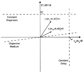
FIG. 2 illustrates a vector diagram of dispersion parameters.
FIG. 3 illustrates a chromatic dispersion compensator, according to an
embodiment.
FIG. 4 illustrates another chromatic dispersion compensator, according to an
embodiment
FIG. 5 illustrates another chromatic dispersion compensator, according to an
embodiment.
FIG. 6 illustrates another chromatic dispersion compensator, according to an
embodiment.
FIG. 7 illustrates a cross-section of a waveguide, according to an embodiment.
FIG. 8 is a flow chart of a method, according to an embodiment.
Embodiments of the present invention will be described with reference to the
accompanying drawings.
DETAILED DESCRIPTION
Although specific configurations and arrangements are discussed, it should be
understood that this is done for illustrative purposes only. A person skilled
in the
pertinent art will recognize that other configurations and arrangements can be
used.
It will be
. apparent to a person skilled in the pertinent art that this invention can
also be
employed in a variety of other applications.
It is noted that references in the specification to "one embodiment," "an
embodiment,"
"an example embodiment," etc., indicate that the embodiment described may
include
a particular feature, structure, or characteristic, but every embodiment may
not
necessarily include the particular feature, structure, or characteristic.
Moreover, such
phrases do not necessarily refer to the same embodiment. Further, when a
particular
feature, structure or characteristic is described in connection with an
embodiment, it
would be within the knowledge of one skilled in the art to effect such
feature,
structure or characteristic in connection with other embodiments whether or
not
explicitly described.
Embodiments of the invention described herein offer a solution to the problem
of
chromatic dispersion in optical coherence tomography by using, for example,
physical
CA 02830177 2013-09-13
WO 2012/123122 PCT/EP2012/001161
- 5 -
equalization that is suitable for integration through microfabrication
techniques. One
embodiment includes a sequential combination of waveguide segments with
different
dispersive properties, in such a way that the resulting chain has a desired
dispersion
behavior. A multiplicity of waveguide segments may be formed by chosen
combinations of different waveguide lengths and types. A multiplexing
configuration
may be used to obtain selectable dispersion coefficients. The multiplexing can
be of
different types, including, for example, time-domain and frequency domain
implementations. In an embodiment, the chromatic dispersion compensation
system
may be placed in the reference and/or sample arm of an interferometer to offer
physical dispersion adjustment.
Embodiments of the invention described herein compensate for dispersion while
solving the specific difficulties of integrated waveguide systems and
profiting from
their specific advantages. In one example, the embodied chromatic dispersion
compensator is different from systems based on the introduction of macroscopic
dispersive materials in free-space environments, as it does not require
collimating
elements, thereby producing a solution that does not interrupt the guided-wave
optical path. In another example, the embodied chromatic dispersion
compensator is
different from numerical systems because it produces actual physical
dispersion
equalization between both optical arms and can be used for compensation of
much
larger mismatches. In another example, the embodied chromatic dispersion
compensator is different from solutions based on macroscopic dispersive
elements
because it does not require external optical elements and may be integrated in
planar
optical devices. Compared to numerical systems, the embodied chromatic
dispersion
compensator has an advantage of a larger working range without impacting
signal to
noise ratio.
FIG. 1 illustrates an OCT system 101, utilizing an optical compensating
element 112,
and used for imaging a sample 110, according to an embodiment. For example,
optical compensating element 112 may compensate for chromatic dispersion of
the
light within OCT system 101. The use of the term "light" may refer to any
range of
the electromagnetic spectrum. In an embodiment, the term "light" refers to
infrared
radiation at a wavelength of around 1.3 pm.
OCT system 101 further includes an optical source 102, a splitting element
104, a
sample arm 106, a reference arm 108, and a detector 114. In the embodiment
shown, compensating element 112 is located within reference arm 108, however,
it
CA 02830177 2013-09-13
WO 2012/123122 PCT/EP2012/001161
- 6 -
should be understood that compensating element 112 may also be located in
sample
arm 106. Alternatively, compensating element 112 may be present in both sample
arm 106 and reference arm 108. In one example, sample arm 106 and reference -
arm 108 are optical waveguides such as patterned waveguides or optical fibers.
In
an embodiment, all of the components of OCT system 101 are integrated onto a
planar lightwave circuit (PLC). Other implementations may be considered as
well,
such as, for example, fiber optic systems, free-space optical systems,
photonic
crystal systems, etc.
It should be understood that OCT system 101 may include any number of other
optical elements not shown for the sake of clarity. For example, OCT system
101
may include mirrors, lenses, gratings, splitters, micromechanical elements,
etc., along
the paths of sample arm 106 or reference arm 108.
Splitting element 104 is used to direct light received from optical source 102
to both
sample arm 106 and reference arm 108. Splitting element 104 may be, for
example,
a bi-directional coupler, an optical splitter, or any other modulating optical
device that
converts a single beam of light into two or more beams of light.
Light that travels down sample arm 106 ultimately impinges upon sample 110.
Sample 110 may be any suitable sample to be imaged such as tissue. During an
OCT procedure, the light scans at a certain depth within sample 110 and the
scattered radiation is collected back into sample arm 106. In another
embodiment,
the scattered radiation is collected back into a different waveguide than the
transmitting waveguide.
Light within sample arm 106 and reference arm 108 is recombined before being
received at detector 114. In the embodiment shown, the light is recombined by
splitting element 104. In another embodiment, the light is recombined at a
different
optical coupling element than splitting element 104.
Compensating element 112 may be designed to compensate for a changing
chromatic dispersion of the light within sample arm 106 that results from
scanning at
various depths within sample 110. Thus, in an example, compensating element
112
affects the optical properties of light in reference arm 108 to compensate for
a
chromatic dispersion associated with the light in sample arm 106. Various
embodiments of compensating element 112 are described herein.
CA 02830177 2013-09-13
WO 2012/123122 PCT/EP2012/001161
- 7 -
An active dispersion compensation system, such as compensating element 112 in
one example, includes a plurality of optical paths composed of waveguide
segments
with different group delay and dispersion properties. This divergence in
properties
may result from, for example, different geometries, different core and
cladding
materials, periodic or quasi-periodic etching, and different doping patterns
inducing
dispersive properties (e.g. photonic crystals, Bragg diffraction gratings) in
the light
guiding region, or otherwise. Each of the waveguide segments may be
characterized
by a different effective refractive index. A change in the properties
described above
causes a change in the effective refractive index. In an embodiment, the
number of
segment types depends on the highest order of the chromatic dispersion to
compensate for, with two types being the minimum number to adjust arbitrary
combinations of group delay and second order dispersion. For example,
compensating for 4th order dispersion utilizes a waveguide having four segment
types. If there is a mismatch between the size and/or shape of the modes
travelling
in the different segments, mode spot size converters may be used to ensure
adiabatic coupling between the various segments. Examples of such spot size
converters include vertical and/or horizontal waveguide tapers.
In order to equalize or compensate for any combination of dispersion
coefficients and
group delay, vectors formed by the dispersion coefficients per unit length and
the
group delay per unit length of each waveguide type form a generating system of
the
vector space of coefficients to compensate for a given chromatic dispersion.
For the
final system to be compact in the general case, the vectors should exhibit
sufficient
linear independence.
In one embodiment, the dispersion and group delay vectors form an n-
dimensional
vector space, with ft being the highest dispersion order for compensation. For
n=2,
the two waveguide types are represented by two vectors formed by the unit
coefficients corresponding to group delay and second order dispersion. If
these
vectors are non-collinear then any point in the plane can be expressed as
their linear
combination. This is expressed formally in Equation 1 below:
(Tg drgli di CIT92/ di) (11)
D2) / dl dD?Idl)k12) (1)
CA 02830177 2013-09-13
WO 2012/123122 PCT/EP2012/001161
- 8 -
Equation 1 shows that any combination of delay (Og) and dispersion (02) can be
attained through concatenation of two waveguide segments of adequate lengths
01,
02. There are areas in the plane implying negative lengths for some waveguide
types, but for all effects, what matters in OCT is the phase difference
between the
reference and sample arm. Therefore, negative lengths in one arm can be
understood to be positive lengths in the opposite arm.
In an embodiment, for any chosen optical path, waveguide segments with
different
properties have a set of unique lengths. In one example, the lengths are
calculated in
such a way that all switchable paths introduce the same total group delay. In
another
example, the lengths are calculated in such a way that each of the paths has a
different group delay (e.g. linearly spaced) but constant dispersion. In the
latter
example, it is possible to obtain a significant free-space scan range without
suffering
from waveguide related chromatic dispersion.
FIG. 2 illustrates a vector diagram using a Cartesian coordinate system of an
example case, where chromatic dispersion is compensated to second order (n=2).
In
the diagram, the x-axis represents group delays (and velocities) and the y-
axis
denotes the amount of group delay dispersion (GOD), and consequently, the
group
velocity dispersion (GVD). In FIG. 2, two different waveguide segments are
represented by two vectors, which are formed by the two corresponding unitary
coefficients.
=
FIG. 2 also illustrates areas defined by combinations of group delay and GOD
corresponding to specific selection strategies for the effective refractive
index of the
waveguide segments. For example, the case where the selection of the effective
refractive index of the waveguide segments leads to a constant group delay but
varying GDD is illustrated as a vertical line with constant delay. In another
example,
the case where the selection of the effective refractive index of the
waveguide
segments results in each optical path inducing a different group delay and a
constant
GOD is illustrated as a horizontal line of constant dispersion. Also
illustrated is an
angled line whose slope is given by the relationship between group velocity
and
group velocity dispersion for a given dispersive medium, when probing various
depths of the medium without dispersive effects.
FIG. 3 illustrates a chromatic dispersion compensator system, according to an
embodiment. = The system includes a plurality of switching elements 1, a
plurality of
CA 02830177 2013-09-13
WO 2012/123122 PCT/EP2012/001161
- 9
waveguides each comprising two segments 2 and 2', a plurality of modulating
elements 3, and a plurality of reflective elements 4.
An active optical path 5 (shown in bold) may be identified using plurality of
switching
elements 1. Each of switching elements 1 may be, for example, an optical
switch or
any modulating element that directs a majority of the incident light down one
path
instead of another. Each of the eight optical paths illustrated includes a
waveguide
having a unique combination of waveguide segments 2 and 2'. For example, each
of
segments 2 and 2' may be identified by a change in the waveguide width, doping
profile, material, or any factor that causes a change to the effective
refractive index of
the particular segment.
In the case of optical coherence tomography, it is undesirable if switching
elements 1
allow small but significant components of optical power to reach optical paths
other
than the active optical path 5. The leaked light produces a contribution to
the
interference pattern that appears as a perturbation source. Thus, in an
embodiment,
modulating elements 3 are placed in each optical path, with the purpose of
applying a
specific modulation (e.g. phase/frequency) to active optical path 5 and
shifting the
spectrum of its interference pattern as measured at a photodetector. In this
way,
considerable suppression of such interference sources can be obtained.
Modulating
element 3 may be a phase modulator and configured to suppress any interference
between the various optical paths due to non-ideal light switching in
switching
elements 1.
In the embodiment illustrated, each optical path also includes reflective
element 4.
The light incident upon reflective element 4 may be returned back through the
same
optical path 5. Reflective element 4 may be a mirror or polished facet.
In one example, each optical path of the chromatic dispersion compensator
illustrated
in FIG. 3 may be chosen to compensate for a different level of chromatic
dispersion
present within light returning from sample 110 through sample arm 106. Various
levels of chromatic dispersion may result from various scan depths within
sample
110, and the resulting chromatic dispersion can be predetermined for the
various
scan depths. In an embodiment, plurality of reflective elements 4 are situated
at the
end of reference arm 108 of OCT system 101.
Although eight optical paths are illustrated, any number of optical paths may
be
realized along with any suitable multiplexing means for identifying amongst
the paths
CA 02830177 2013-09-13
WO 2012/123122 PCT/EP2012/001161
- 10 -
as would be understood by one having skill in the relevant art(s) given the
description
herein. Furthermore, although a time-division multiplexing scheme has
been
illustrated using switching elements 1, it is also possible to implement a
frequency-
division multiplexing scheme using phase modulators to identify more than one
optical path simultaneously.
FIG. 4 illustrates another embodiment of a chromatic dispersion compensator.
Instead of including reflective elements 4, the illustrated embodiment
includes a
duplicate arrangement of optical paths and switching elements 1 on an opposite
side
of the plurality of waveguides. The duplicate arrangement may guide the
dispersion-
compensated light back to splitting element 104 and/or detector 114. In
another
example, a second network of optical paths are provided which do not mirror
the
arrangement of the first network of optical paths from which active optical
path 5 is
chosen. Such a transmission configuration as illustrated may be useful when
placed
within sample arm 106 of OCT system 101, according to an embodiment.
FIG. 5 illustrates another embodiment of a chromatic dispersion compensator
that
does not include modulating elements 3. Additionally, each waveguide disposed
along each optical path includes 3 waveguide segments 2, 2', 2", according to
an
embodiment. The use of three waveguide segments 2, 2', 2" allows for third
order
chromatic dispersion compensation (n=3).
Although previous figures illustrate switching elements 1 forming a binary
tree for the
identification of the desired waveguide within the plurality, it is possible
to consider
other architectures for path identification. In one example, optical switches
may be
used to inject light at different points in common waveguide segments. In
another
example, concatenation of various waveguide segments is done using switching
elements 1.
FIG. 6 illustrates an implementation where optical path identification is done
through
a configuration of switching elements 1 arranged in a cascade, according to an
embodiment. Switching elements 1 allow for selecting between waveguide
segments
2 and 2' of different type at each stage of the cascade. Through the actuation
of
these switches, it is possible to direct optical power to one active optical
path 5
between the 2n possible optical paths, where n is the number of stages in such
a
cascaded configuration. If the design of the lengths of waveguide segments 2,
2' in
each alternative branch is adequate, it is possible to obtain a set of
distinct points in
CA 02830177 2013-09-13
WO 2012/123122 PCT/EP2012/001161
- 11 -
the vector space defined by the group delay and dispersion coefficients of
interest,
according to an embodiment. In the embodiment shown, branch selection is
binary,
but switching elements 1 with more than two inputs and outputs can be
considered
for the compensation of higher dispersion orders.
The embodiments described above utilize waveguides with various segments
identified by vectors formed by group delay and dispersion coefficients per
unit
length. The design and fabrication of such waveguides are described in more
detail
herein.
In an embodiment, rib/ridge waveguides are used because they allow for a
moderately large mode size while retaining single--mode operation. The rib
geometry is shown in FIG. 7, where its defining parameters are illustrated.
The refractive indices of a substrate ns and a cladding nc are lower than the
index
of a wavegyiding region nf. The relationship between a rib height H and a slab
thickness h is often expressed in terms of a dimensionless parameter: = rH.
Conditions for single mode operation within a waveguide have been presented
previously in the literature. Single mode operation may be obtained when using
rectangular waveguides with a width and a height less than around 2 microns.
Compared to rectangular or strip waveguides, rib/ridge waveguides allow for
low-loss
guiding (<1dB/cm) as long as some effort is devoted to sidewall smoothing.
Different waveguide geometries have been studied using a program based on the
Beam Propagation Method (BPM). BPM solves the Helmholtz equation under a
slowly varying envelope approximation. This method is able to provide
reasonably
accurate solutions of the fundamental (and higher) modes in a waveguide from
its cross-section. For each mode, an effective refractive index can be
obtained,
associated with a given propagation constant. By
sweeping the excitation
wavelength, the spectral behavior of the mode is recovered. The dispersive
properties of the material are not considered in the simulations, as the
results contain
the geometric contribution only. Indeed, intramodal dispersion is
traditionally split
into a component due to the waveguide behavior Dw and another component
due to bulk properties of the material Dm. Although this example simulation is
used
herein for reference, one of skill in the art will recognize that other
techniques and
geometric values may instead be used.
CA 02830177 2013-09-13
WO 2012/123122 PCT/EP2012/001161
- 12 -
In this example simulation, dispersion coefficients are extracted from a
polynomial fit
corresponding to the Taylor expansion of the propagation constant as a
function of
angular frequency, as shown below in Equation 2.
a2n(w) 1 (33fl(a))
ig((0) = ig0agw) ((0 (00) + 2! OP,02 __ (W WO)2 + (a) ¨ 0)0)3 + (2)
aw
= The first three terms of the expansion (other than the constant) are the
group velocity,
group velocity dispersion (GVD), and the third order dispersion, respectively.
In the
following analysis only the first two terms are targeted for design purposes.
The simulated geometries are grouped into a first category complying with the
standard single-mode condition and then into another birefringence-free
category.
For all geometries, a sensitivity analysis is performed with respect to the
lateral
dimension. Then, for a candidate waveguide technology, variations in all
design
parameters subject to manufacturing tolerances for waveguide dimensions H, W,
h
and the core refractive index have been introduced, taking into account
possible
temperature changes inducing thermo-optical shifts.
Different geometries are chosen for various waveguide segments. An example of
chosen geometries for seven example waveguide segments are shown below in
Table 1.
Table 1
Geometry W (gm) H (pm) h (pm)
A 5.4 6.0 4.60 0.77
2.7 3.0 2.30 0.77
1.35 1.5 1.03 0.69
1.35 1.5 1.21 0.81
0.9 1.0 0.77 0.77
0.63 0.7 0.53 0.76
0.4 0.4 0.31 0.77
CA 02830177 2013-09-13
WO 2012/123122 PCT/EP2012/001161
- 13 -
The chosen geometries cover a range of waveguide dimensions from larger
dimensions as shown in segment A down to sub-micron dimensions in segment G.
The obtained GVD and group delay are summarized in Table 2 below for each
waveguide segment and for both the quasi-TE and quasi-TM modes.
Table 2
Quasi-TE Quasi-TM
Geometry 1/vg GVD 1/vg GVD
Ifs/cm] [fs/(cm=nm)] Ifs/cm] [fs/(cminm)]
A 116732.86 0.10 116737.54 0.11
116930.40 0.37 116966.07 0.45
117558.69 1.13 117816.56 1.69
117401.80 0.94 117640.06 1.46
118361.64 1.94 119148.68 3.61
119422.10 2.64 121511.14 6.94
121348.09 2.00 129551.30 38.41
Table 2 shows that the waveguides are somewhat birefringent in terms of group
velocity, but this effect is exaggerated with regard to dispersion when
dimensions
decrease. Ideally, in the embodied OCT system, dispersion compensation is
performed for amounts starting at 27fs and going up to 270fs (corresponding to
a 10
mm scan range). This requires dispersion levels in the range of 1-3fs/(cm-nm)
so
that compensation can be achieved over a waveguide with a maximum total length
of
around 1 cm over an optical bandwith up to 100nm, allowing for a more compact
physical implementation. These geometric dispersion levels can be attained
with
waveguides of around 1pm in size, but the differences between both
polarization
modes become too large for such shallow etch designs (factor of 2 difference
or
higher). Regarding manufacturing sensitivity, studies performed with respect
to line
width W yield reasonable stability down to waveguides with mode dimensions
around
1pm.
As discussed, changing either of the geometric dimensions H, h, W and/or
refractive
index of the waveguide material will change the group velocity (inverse of the
group
delay) and the GVD associated with the waveguide. Fabrication imperfections
will
have an impact on all of these variables. Table 3 below summarizes how
sensitive
CA 02830177 2013-09-13
WO 2012/123122 PCT/EP2012/001161
- 14 -
both group velocity and GVD are to changes in these parameters for each
polarization mode in a silicon waveguide having H = 1.5 urn, W = 0.8 urn, and
r =
0.39.
Table 3
Polar. Variable S(GVD) S(l/vg)
TE ns, = -0,34 0,98
TE H -1,21 -0,03
TE h -1,06 -0,02
TE W. -0,07 -0,01
TM ns, -0,19 0,98
TM H -1,46 -0,03
TM h -0,13 -0,01
TM W -0,54 -0,02
It was found that the core refractive index is the only parameter that has a
significant
influence on group velocity, and the calculated sensitivity is close to 1.
This is not
unexpected given the strong field confinement in the core. Geometric
parameters
change the dispersion relation slightly, but its slope is still dominated by
the material.
Both polarizations exhibit the same behavior regarding the impact of
perturbations on
group velocity.
Overall, for this example simulation, reasonably stable behavior is observed
in the
dispersion coefficients. The largest sensitivity in absolute value is 1.46.
Expected
changes in the parameters are summarized below in Table 4, along with the
estimated effect on GVD for each polarization. The assumed refractive index
' variation is consistent with a temperature excursion of around 80K.
Vertical
dimensions have been estimated from experience with common cleanroom
processes. Accurate parameter tuning and the introduction of metrology and
corrective process steps may further improve these values. A variation in
waveguide
width of 100nm has been chosen as an acceptable fabrication tolerance.
CA 02830177 2013-09-13
WO 2012/123122 PCT/EP2012/001161
- 15 -
Table 4
Variable Ax Ax/x Polar. AGVDIGVD Avglvg
TE -0.20% -0.56%
ns, 0.02 0.58%
TM -0.10% -0.56%
TE -4.03% 0.09%
50nm 3.33%
TM -4.88% 0.10%
TE -9.05% 0.15%
50nm 8.55%
TM -1.11% 0.04%
TE -0.88% 0.11%
100nm 12.50%
TM -6.78% 0.19%
The calculated sensitivities shown in Table 4 may be used to update the
waveguide
dimensions to obtain better polarization independence regarding dispersion.
For
example, width W may be increased by 10% to 0.88pm while h may be decreased by
5% to 0.55pm. These example parameters allow nearly independent modification
of
the properties of each polarization mode. A repetition of the previous BPM-
based
analysis for this new geometry leads to a GVD of 2.633 fs/(cm-nm) for the TE
mode
and a GVD of 2.616 fs/(cm-nm) for the TM mode.
FIG. 8 illustrates an example method 800 for compensating for chromatic
dispersion,
according to an embodiment. Method 800 may be performed by various components
of OCT system 101, which may include a chromatic dispersion compensator such
as
those illustrated in FIGs. 3-6.
At block 802, a beam of radiation is split to form at least a first and second
beam of
radiation. The beam of radiation may be split, for example, via an optical
splitter or a
bi-directional coupling device. Any or all of the beams of radiation may be
confined
within waveguides such as optical fibers, strip waveguides, or rib/ridge
waveguides.
At block 804, one or more optical paths is identified amongst a plurality of
optical
paths. The identifying may be performed by an optical switch. Alternately, the
identifying may be performed by optical circulators or phase modulators.
CA 02830177 2013-09-13
WO 2012/123122 PCT/EP2012/001161
- 16 -
At block 806, the first beam of radiation is received through the identified
one or more
optical paths.
At block 808, at least one of a group delay and dispersion is introduced to
the first
beam of radiation through the identified one or more paths. The group delay
and
dispersion introduced to the first beam of radiation through the identified
one or more
paths is different than a group delay and dispersion that would have been
introduced
to the first beam of radiation through another one or more paths amongst the
plurality
of optical paths. Additionally, the group delay and dispersion form a
generator of the
vector space of coefficients to compensate for a chromatic dispersion
associated with
the second beam of radiation.
It is to be appreciated that the Detailed Description section, and not the
Summary
and Abstract sections, is intended to be used to interpret the claims. The
Summary
and Abstract sections may set forth one or more but not all exemplary
embodiments
of the present invention as contemplated by the inventor(s), and thus, are not
intended to limit the present invention and the appended claims in any way.
Embodiments of the present invention have been described above with the aid of
functional building blocks illustrating the implementation of specified
functions and
relationships thereof. The boundaries of these functional building blocks have
been
arbitrarily defined herein for the convenience of the description. Alternate
boundaries
can be defined so long as the specified functions and relationships thereof
are
appropriately performed.
The foregoing description of the specific embodiments will so fully reveal the
general
nature of the invention that others can, by applying knowledge within the
skill of the
art, readily modify and/or adapt for various applications such specific
embodiments,
without undue experimentation, without departing from the general concept of
the
present invention. Therefore, such adaptations and modifications are intended
to be
within the meaning and range of equivalents of the disclosed embodiments,
based on
the teaching and guidance presented herein. It is to be understood that the
phraseology or terminology herein is for the purpose of description and not of
limitation, such that the terminology or phraseology of the present
specification is to
be interpreted by the skilled artisan in light of the teachings and guidance.
CA 02830177 2013-09-13
WO 2012/123122 PCT/EP2012/001161
- 17 -
The breadth and scope of the present invention should not be limited by any of
the
above-described exemplary embodiments, but should be defined only in
accordance
with the following claims and their equivalents.