Note: Descriptions are shown in the official language in which they were submitted.
CA 02830905 2013-09-20
WO 2013/066270
PCT/SG2012/000415
SYSTEM AND DEVICE FOR DRIVING A PLURALITY OF HIGH
POWERED LED UNITS
FIELD OF THE INVENTION
The present invention relates to a system and device for driving a plurality
of high-
powered light emitting diodes (LED) units. The device is particularly
suitable, but not
limited for use in high powered LED light units such as down lights, T5, T8,
Light
Troffer, Hi-Bay lamps and MR16 light bulbs etc.
BACKGROUND TO THE INVENTION
The following discussion of the background of the invention is intended to
facilitate
an understanding of the present invention. However, it should be appreciated
that the
discussion is not an acknowledgement or admission that any of the material
referred
to was published, known or part of the common general knowledge in any
jurisdiction
as at the priority date of the application.
Conventional lighting systems typically have a configuration where light
products
used in the systems are individually driven. For example, a light product such
as a
down light lamp has its own in-built power supply or ballast which converts
incoming
AC electrical supply to higher AC voltage and desired current that is required
to
provide electrical power to for example ignite and excite the gases (referring
to CFL
light) for lighting up of the down light. Examples of such other light
products include
T5, T8, Light Troffer, High-Bay lamps, street lamps and flood lamps.
Similarly, when Light Emitting Diodes (LEDs) were introduced in lighting
systems,
the configuration adopted for LEDs was based on a similar 'one-ballast
(controller)'
to 'one-lamp' arrangement of conventional lighting systems. Therefore, each
LED
light unit has its own in-built LED driver or controller that converts the
incoming AC
supply to DC voltage and current to light up the LED down light. This means
that
each LED light unit that is present in a lighting system has an accompanying
controller dedicated to that particular LED light unit for converting the
incoming AC
supply to DC voltage and current for lighting up that particular LED light
unit, i.e. a
1
CA 02830905 2013-09-20
WO 2013/066270
PCT/SG2012/000415
chain of ten LED down lights in a lighting system will require correspondingly
ten
LED controller circuits. These LED controllers increase the cost and overall
form
factor of each lamp unit.
A prior art LED light unit and system is illustrated in Fig. 1 and Fig. 2
respectively.
The LED lamp unit comprises an AC source supply via AC Input Terminal 4, an AC-
DC LED driver 3, a LED light/lamp module 1 and heat sink 2.
When connected, AC electrical supply current will flow to the input of the AC-
DC
LED driver 3. The AC supply current will be rectified via switch mode power
supply
circuitry in the AC-DC LED driver 3 to supply the desired DC voltage and
current to
the LED light module 1. For continuous light-up operation, as heat will be
generated
by both the AC-DC LED driver 3 and the LEDs on the LED light module 1,
introduction of heat sink 2 is important to ensure the heat generated along
the light-up
operation is drawn from the heat source and dissipated accordingly. The heat
sink 2
has to account for heat dissipation from both the LED light module and AC-DC
LED
driver. Consequently, if at any time along the light-up operation the heat
sink 2
reaches its maximum heat dissipation capability due to the design limitation
in size for
standard form factor for the particular LED lighting unit fulfillment will
lead to the
degradation of light performance and product life span.
The above-mentioned configuration has several disadvantages listed as follows:
= As each LED light unit requires its own in-built controller circuit 3 for
lighting
up, when the LED light unit is in continuous operation, considerable heat will
be generated by both the LED and controller circuit. To moderate the heat,
heat sink(s) must be present in each LED light unit for drawing the heat from
the heat source and dissipating the heat to the surroundings so as to provide
a
thermally cool environment for the LED and controller circuit to operate in.
It
is important that the LED and controller circuit operate in a thermally cool
environment because this will reduce power loss and hence improve
efficiency. However, due to standard form factors, there is a limit as to the
size of the heat sink in each LED light unit. As there are two heat generating
sources in each LED light unit (i.e. the LED lamp unit and the LED
2
CA 02830905 2016-02-03
controller), the heat sink 2 typically reaches its maximum heat dissipation
capability
during continuous operation where considerable heat is generated.
Consequently, this
will lead to the degradation of the LED light unit's light performance and
product life
span.
= It is typically costly to manufacture LED light units which have built-in
controller
circuits and heat sinks 2 as they increase the number of components that are
needed for
manufacture. Furthermore, the heat sink must also be designed to cope with the
dissipation of heat from two heat sources with the constraints on its size due
to standard
form factors. This further increases the overall cost of producing the LED
light units.
= As the AC supply will be converted to DC voltage and current in the LED
light units by
the controller circuits 3, there will be safety related issues that must be
addressed. Hence,
the LED light units will have to be designed such that they meet the standard
safety
requirements and size limitations imposed by standard form factors.
Therefore, it may be desirable to overcome, or at least alleviate, one or more
of the
aforementioned problems.
SUMMARY OF THE INVENTION
In one aspect, the present disclosure provides a system and device to
alleviate the above
problems and to provide a 'one driver-to-many high powered LED lamp units'
solution. To
achieve the same, the system and device are suited to provide at least a
relatively 'ripple
free' current of less than 5% from the specified rated current. The specified
rated current is
typically (but not limited to) around 350 mA to 700 mA per lamp unit.
In addition, references to 'current', 'connection(s)' refer to electrical
current and
connections unless otherwise stated.
In accordance with a first aspect of the present invention there is a system
for driving a
plurality of high powered LED units, the system comprising a single driver for
providing
ripple free direct current to a plurality of high powered LED lamp units, the
single driver
3
CA 02830905 2016-02-03
arranged to operate in an isolated alternating current fly back configuration
having an
inductive element as a transformer isolating the plurality of high powered
LEDs at a
secondary end of the transformer, wherein the single driver further comprises
a digital
controller having an electronic oscillator for providing a clock cycle, the
digital controller
programmable to adjust the ripple free direct current at every clock cycle
based on detection
and computation of a duration taken for an amount of energy to be discharged
by the
transformer to the plurality of high power LED lamp units.
Preferably, the single driver operates in an isolated alternating current fly
back configuration
having an inductive element as a transformer isolating the plurality of high
powered LEDs at
the secondary end of the transformer.
Preferably the digital controller is an Application Specific Integrated
Circuit (ASIC); the
ASIC further operable to detect and compute the duration of the energy
discharged by the
core of transformer to the plurality of high powered LEDs to regulate and
provide the ripple
free output DC current. The ASIC is preferably programmed to receive feedback
at each
clock-cycle based on the duration of the energy discharged by the core of the
transformer as
an input to determine the amount of ripple free constant DC current at the
next clock-cycle.
More preferably the ASIC is programmed to provide a voltage waveform to turn
an
electronic switch on and off at each clock-cycle.
Preferably each of the plurality of high powered LED lamp units is in series
with the other
high powered LED lamp units.
Preferably the single driver is electrically connected to a dimmer circuitry
for adjusting the
brightness of the plurality of high powered LED lamp units. The dimmer
circuitry preferably
comprises a potential meter, infra-red interface, motion sensor or ambient
sensor.
Preferably the system comprises a filter capacitor operable to vary its
capacitance to
maintain a power factor of at least 0.9 when the dimmer is adjusted.
4
CA 02830905 2016-02-03
In the case where the dimmer is a potential meter, the potential meter is
operable to work
within a voltage of 0 to 10V.
Preferably in an isolated fly back mode the secondary end of the transformer
is electrically
connected to a short circuit protection circuit.
Preferably, the ASIC is coupled with an active power factor controller. More
preferably the
active power factor controller comprises at least one voltage follower. In
such a case the
ASIC is preferably a 14-pin configuration so as to control both the active
power factor
controller and the adjustment of the ripple-free constant DC current.
Preferably, each high powered LED lamp is provided with a heat sink shaped and
configured to dissipate heat away from the high powered LED only.
Preferably, the system further comprises an electronic switch, wherein the
ripple free
constant DC current is achieved by means of voltage control according to the
following
equation:-
VIN = TON r;
V
Your ¨ _________
TOFF Li
Where YouT is the voltage across the output; YIN is the input voltage; TOFF is
the time of the
discharge of the core of the isolating transformer; TON is the switch on time
of the electronic
switch; L1 is the inductance value of the primary windings of the transformer
and L2 is the
inductance value of the secondary windings of the transformer.
As an alternative to the isolated configuration mode, the single driver may
operate in a non-
isolated configuration having an inductive element operating in a continuous
mode in
according to the following equation:-
5
CA 02830905 2016-02-03
bur TOFF 1
/ow. (Torr _______________________ )* --
2
where TOFF is fixed as a constant; TON is the switch on time of the electronic
switch; T is the
summation of TON, TOPE, and TCALC where TCALC is the time after the discharge
time of the
inductive element to compute the formula; II is the desired reference current
and 'MAX is the
peak current. In a hysteretic controller configuration, the value of /MAX and
Li may be fixed,
and the TON and TOFF timings determined.
In an embodiment, there is provided a system for driving a plurality of high
powered LED
units, the system comprising a single driver for providing ripple free direct
current to a
plurality of high powered LED lamp units, wherein the single driver comprises
a digital
controller having an electronic oscillator for providing a clock cycle; the
digital controller
programmable to adjust the ripple free direct current at every clock cycle
based on
determination of a duration taken for an amount of energy to be discharged to
the plurality
of high powered LED lamp units; the single driver further arranged to operate
in an non-
isolated configuration having an inductive element operating in a continuous
mode in
according to the following equation:-
IA/-I * TOI I 1
IOU/ = (T011 * Ii + ______ )*
2
where TOFF is fixed as a constant; TON is a switch on time of the electronic
switch; T is a
summation of TON, Toff, and TCALC where TCALC is a time after the discharge
time of the
inductive element to compute the formula; It is a desired reference current
and 'MAX is the
peak current
In accordance with a second aspect of the invention there is a single driver
as described
above comprising:
6
CA 02830905 2016-02-03
at least one Integrated Circuit (IC), the IC programmable using a hardware
description
language; a first electronic switch operable to provide a first switching time
period to control
power factor voltage, the first switching time period programmable by the at
least one IC;
and a second electronic switch operable to provide a second switching time
period to
regulate ripple free direct current flowing into at least one high powered LED
lamp unit, the
second switching time period is programmable by the at least one IC.
Preferably, the first and second electronic switches are power MOSFETs.
Preferably, the at least one IC is an ASIC.
In accordance with a third aspect of the invention there is a device having an
input port
operable to be connected to a single driver disclosed herein, and a plurality
of output ports,
and comprising a reverse polarity protector arranged to be electrically
connected to the input
port and each of the plurality of output ports; and a plurality of open
circuit protection
circuits, each of the plurality of open circuit protector operable to connect
to an output port;
wherein the reverse polarity protector is operable to negate the polarity
requirement in the
event where a load is connected with a wrong polarity to any of the output
port; and the
open circuit protection circuit is operable to form a closed loop series
connection in the
event where no load is connected to an output port or when a load breaks down.
Preferably the reverse polarity protector is a diode bridge rectifier.
Preferably each output port comprises a corresponding open circuit protector.
Preferably the input port is suitable for connection with a LED driver and
each of the output
port is suitable for connection with a load comprising a high powered LED lamp
unit.
6a
CA 02830905 2014-04-30
In accordance with a fourth aspect of the invention there is a system
according to the first
aspect wherein the load is in a series connection, further comprising the
device according to
the second, or third aspect; wherein the input port of the device is operable
to be connected
to the single driver.
In accordance with a fifth aspect of the invention there is a dimmer circuitry
for use with a
LED driver as disclosed herein, the dimmer circuitry comprising at least a
dimming
interface operable to connect to at least one dimming controller; and a
capacitive element
adjustable to maintain a power factor of at least 0.9 within the dimmer
circuitry.
BRIEF DESCRIPTION OF THE DRAWINGS
The following invention will be described with reference to the following
drawings of
which:
Fig. 1 is a perspective side view of a prior art LED lamp unit with driver and
heat sink;
Fig. 2 is a system configuration of the 'one driver one lamp unit'
configuration of the prior
art LED lamp system;
Fig. 3 is a system view of a 'one driver multiple lamp units' or 'string
driver' in accordance
to an embodiment of the invention;
Fig. 4 is a circuit diagram of the LED driver circuit in accordance with an
embodiment of
the invention for isolated alternating current (AC) application;
Fig. 5a and 5b are circuit diagrams of the LED driver circuit with a power
factor converter
driven by a 14-pin ASIC in accordance with another embodiment of the invention
for
isolating alternating current (AC) application;
Fig. 6 is a table summarizing the advantages of the invention on a plurality
of MR 16 LED
lamp as compared to the prior art system;
7
CA 02830905 2013-09-20
WO 2013/066270
PCT/SG2012/000415
Fig. 7 illustrates simulation results of the ripple free constant DC current
based on a
MR16 load;
Fig. 8 illustrates another embodiment with an arrangement of circuit wherein
the
decoupling transformer operates in a continuous mode;
Fig. 9 illustrates electrical current flowing through rectifier circuitry in a
continuous
mode;
Fig. 10 illustrates a structure of hysteretic controller used for continuous
operation of
the circuit;
Fig. 11 is a PCB arrangement of an intermediary connector between the LED
drivers
and load in accordance with another embodiment of the invention;
Fig. 12 is a possible arrangement of a lighting system illustrating the use of
an
intermediary connector between the driver and load;
Fig. 13 is another possible arrangement of a lighting system illustrating the
use of
two intermediary connectors;
Fig. 14 shows the circuit diagram of the intermediary connector; and
Fig. 15 shows a general block diagram on the dimmer circuitry.
Other arrangements of the invention are possible and, consequently, the
accompanying drawings are not to be understood as superseding the generality
of the
preceding description of the invention.
DETAILED DESCRIPTION OF THE INVENTION
In the context of the invention, the mention of 'ripple free' current and
approximations to ripple free current refers to allowable ripple of less than
(1 5%
from the specified rated current.
In the context of the invention, high powered LED lamp units refer to any LED
lamp
unit requiring a power of at least 5 watts.
8
CA 02830905 2013-09-20
WO 2013/066270
PCT/SG2012/000415
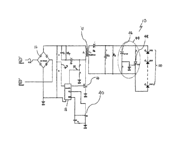
In accordance with an embodiment of the invention there is a LED driver 10 for
driving a plurality of high powered LED lamps 100 as illustrated in Fig. 4.
LED
driver 10 is particularly suited for an isolated alternating current (AC)
application and
comprises a primary side and a secondary side. The primary side of the LED
driver 10
is decoupled with the secondary side via a decoupling transformer 11. The
primary
side comprises an electronic switch 14, bridge rectifier circuit 16, and an
Integrated
Circuit (IC) controller 18. Although Fig. 4 shows an isolated configuration,
it is
appreciated by a skilled person that the circuit may be modified for non-
isolated
configuration where the decoupling transformer 11 may be replaced by other
inductive elements.
To satisfy the decoupling function, transformer 11 is an isolation
transformer, and
may preferably be a planar transformer. Transformer 11 is operable to work in
either
a continuous or discontinuous mode, although for purpose of illustration Fig.
4, 5a,
and 5b illustrates the circuitry suited for transformer 11 working in a
discontinuous
mode. In continuous mode certain output capacitors may be omitted as
illustrated in
Fig. 8 or 10. Where transformer 11 is a planer transformer based on printed
circuit
board technology, the printed circuit board may be FR4 PCB, Polyimide or other
thick
copper foil (lead frame).
Resistor Rp and capacitor Cp are connected in a parallel configuration with
the
primary end of the transformer 11. A diode Dp is connected to the Resistors
Rp,
capacitor Cp, and the transformer 11. The conducting end of the diode Dp is
connected in a series configuration to the primary end of the transformer 11.
The non-
conducting end of the diode Dp is connected in series configuration to the
resistor Rp
and capacitor Cp.
A capacitor Cs is connected in parallel to the secondary end of the
transformer 11 for
filtering the output electrical voltage. A diode Ds is connected to the
secondary end
of the transformer 11 and the capacitor Cs. The conducting end of the diode Ds
is
connected to the secondary end of the transformer 11 in a series
configuration. The
non-conducting end of the diode Ds is connected to the positive end of
capacitor Cs
(where applicable) in a series configuration. The LED load 100 is connected in
a
parallel configuration to the capacitor Cs. Each LED load 100 may be connected
in
9
CA 02830905 2013-09-20
WO 2013/066270
PCT/SG2012/000415
series with the other LED load 100. The secondary side may optionally include
a
short circuit protection circuit 44 as will be elaborated later.
Electronic switch 14 is typically a power transistor. In this particular
embodiment,
electronic switch 14 is more preferably a power MOSFET. In the MOSFET
configuration, the drain of the electronic switch 14 is connected to the
conducting end
of the diode Dp and to the primary end of transformer 11. The gate of the
electronic
switch 14 is connected to the output pin of the IC 18, and the source of the
electronic
switch 14 is connected to the electrical ground.
It is to be appreciated that the electronic switch 14 may be replaced by other
functionally equivalent component.
The IC controller 18 comprises an internal oscillator which is configured to
turn on
the gate of the electronic switch 14 with a particular turn-on time period TON
(switching frequency) for each clock cycle as determined by the internal
oscillator.
IC controller 18 is preferably an Application Specific Integrated Circuit
(ASIC)
programmed to sense and calculate the discharge time of the inductive elements
L1
and L2 as a main input. ASIC 18 is programmed and configured to turn on the
gate of
the electronic switch 14 having a turn on period of TON at each clock cycle
based on
the following inputs:-
(a.) A reference constant K based on the discharge time of the inductive
element L1
and L2;
(b.) Desired output DC ripple free current for LED Iour;
(c.) A digitized voltage value VDD (Tin) tapped and digitized from potential
divider 22,
the potential divider 22 connected in parallel with the bridge rectifier 16;
(d.) A time value TOFF of the discharge of the core of transformer 11 measured
through voltage potential divider 30 and compared to a reference voltage; and
(e.) The switching period T (i.e. the switching period of the electronic
switch 14 as
determined by the oscillator).
CA 02830905 2013-09-20
WO 2013/066270 PCT/SG2012/000415
Using the received five inputs, the IC 18 computes an output TON which is the
switch
on time of the electronic switch 14 mathematically expressed as equation (1).
out * T
TON =
K * V in * Toff (1)
The reference constant K is calculated based on the inductance value of the
primary
and secondary windings of the transformer 11 as described in formula 2.
1
K¨
(2)
where L1 is the inductance value of the primary windings of the transformer 11
and
L2 is the inductance value of the secondary windings of the transformer 11.
The value
of reference K may be stored in a memory within the IC 16. For a non-isolated
direct
current (DC) fly-back configuration, the reference constant K is calculated
according
to the following mathematical expression:-
,
= 1 ¨ (2a)
L3
Where L3 is the inductance value of the inductive element in the fly-back
configuration.
Manipulating equation (1) and (2), 'Our is derived as follows:-
VIN * TON * TOFF
IOUT =(3)
2*VL1 *L2 *T
The IC controller 18 may further comprises a dimming pin coupled to a variable
resistor 40 for performing dimming on the LED load 100. The dimming pin
facilitates the flexibility to perform dimming via various dimming device such
as
potential meter, motion sensor or Infra-red sensor.
The IC controller 18 described above is typically 8-pin. To fine-tune the
level of
control of the IC controller 18, a higher resolution IC controller may be
used. In
11
CA 02830905 2013-09-20
WO 2013/066270
PCT/SG2012/000415
addition to the fine-tune control of a desired ripple free current 'OUT,
active power
factor controller (PFC) to improve the performance of the circuit.
A higher resolution IC controller having capabilities to fine-tune the control
of desired
ripple-free current 'Our and provide active power factor control is described
in
another embodiment below.
Another embodiment of the invention in the form of a LED driver 500 for
driving a
plurality of high powered LED lamp units 100 is illustrated in Fig. 5a and
Fig. 5b
(with emphasis on primary side). LED driver 500 comprises a first electronic
switch
513; a second electronic switch 514; a bridge rectifier circuit 516 and an
integrated
circuit controller 518. LED driver 500 further comprises an active power
factor
controller (PFC) circuitry 520. Comparing with the previous embodiment, the
active
power factor controller (PFC) is operable to form an additional stage of
current
controller to achieve an improved ripple free constant DC current. The
integrated
circuit controller 518 is operable to control the switching frequencies of the
first
electronic switch 513 and second electric switch 514 to achieve a desired
power factor
and output ripple free current Iota.
Integrated IC controller 518 is similar to the IC controller 18 comprising
internal
oscillators, built in Analogue to Digital convertor etc. It additionally
comprises more
pins for further control of the PFC controller. In this embodiment IC
controller 518
comprises 14-pin. The overall resolution is higher (10 bits) thus allowing
better
adjustment and fine-tuning of the switching frequencies for the electronic
switches
513,514 and 'our.
The bridge rectifier 516 is operable to receive an AC input and produces a
rectified
voltage output. The rectified voltage output is passed through a capacitor C4.
C4 is
operable to function as an input voltage filter to further filter the
rectified voltage
from the rectifier circuit 516. Capacitor C4 is connected parallel to
resistors Rs and
R9 and in series with an inductor L4.
Resistors R8 and R9 form an input voltage divider. In operation, the voltage
between
R8 and R9 is tapped as an input voltage (denoted as Vinp) to the ASIC.
12
CA 02830905 2013-09-20
WO 2013/066270
PCT/SG2012/000415
The inductor L4 is connected in series with resistors R10 and R11. Resistors
R10 and
R11 form a PFC voltage divider, which is used to provide the PFC feedback
voltage to
the controller 518 via a T2p pin input for PFC output voltage measurement.
The first electronic switch 513 is connected in series to inductive element L4
and in
parallel to the PFC voltage divider. First electronic switch 513 provides the
variable
frequency to control the PFC output voltage. Both the first electronic switch
513 and
the second electronic switch 514 may be N-channel power MOSFET. The gate of
the
first electronic switch 513 is activated by the ASIC (MOSOUT pin), its drain
is
connected in series with L4 and the source is grounded.
In operation, the controller 518 drives the first electronic switch 513 to
provide the
necessary power factor voltage at the drain of the first electronic switch
513.
It is to be appreciated that the first electronic switch 513 may be replaced
by other
functionally equivalent component.
A power diode D3 is connected in series with inductive element L4. It allows
the
forward pass of the rectified PFC current; which is moderated by the first
electronic
switch 513.
C5 is a capacitive filter for filtering the PFC output voltage.
Inductive element L4 may be a standard inductor as illustrated in Fig. 5a or a
transformer as illustrated in Fig. 5b. For the case where L4 is a transformer,
the
transformer comprises Eip primary inductance and L4s secondary inductance. As
illustrated in Fig. 5b, Lip is connected from pin 1 to pin 6; L4s is connected
from pin 1
to pin 7 of the IC controller 518.
The following equation (4) is applicable to the transformer variant to control
the
output voltage of the PFC:-
L4p V IN * TQ2ou
VPFC, OUT = (4)
L4s TQ2off
13
CA 02830905 2013-09-20
WO 2013/066270
PCT/SG2012/000415
VPFC,OUT is the output voltage of the PFC, L4p is the PFC transformer primary
inductor value, Lu is the PFC transformer secondary inductor value, Vin is the
input
voltage, Twon is the switch on time of the first electronic switch 513, and
TQ20ff is the
discharge time of the PFC transformer. TQ2on is controlled via the MOSOUT pin
of
the controller 518 and Vin and TQ20ff are feedback values used for ensuring
and
verifying that VPFC,OUT properly tracks a desired output voltage VOUT.
Equation (4) is known as a voltage follower, where VPFC,OUT follows \Tour; in
the
sense that after solving the equation, if VPFC,OUT is less than expected
(within
allowable deviation) Twon is increased, otherwise Twon is decreased.
VouT is determined based on the total number of LED units and the desired
current
Iota to be supplied to the LED units.
For the second electronic switch 514, the operation and equations for
adjusting and
calculation lour is identical to that described in equations (1) to (3).
As mentioned above, the secondary side of the LED driver 10, 500 may further
comprise a voltage protection circuit 44. Referring to Fig. 4 for the voltage
protection
circuit which may be incorporated in the secondary side of the LED driver 500
although not explicitly shown in Fig. 5a and 5b, voltage protection circuit 44
comprises a zener diode 46, a silicon controlled rectifier (SCR) 48 and a
resistor 50.
When a short circuit is detected, the zener diode 46 will conduct electricity
thus
enabling the SCR 48 and reducing the output voltage to the LEDs 100.
The LED driver 10, 500 in the context of operation of driving a string of LED
light
units, will be described in the following example:-
To operate the circuit, the variable resistors are adjusted to produce a
voltage value of
N for VR (LED driver 10), or Vinp (for LED driver 500), where value N is an
adjustment of turn on time period TON of the electronic switch 14, 514
corresponding
to the generation of the maximum approximately ripple-free constant current to
drive
a plurality of LED lamp units 100. The decrement or increment of adjustment N
value
will be based on the feedback and cause changes in TON, T directly, thus
varying 'our
14
CA 02830905 2013-09-20
WO 2013/066270
PCT/SG2012/000415
accordingly based on the variable resistor VR to dim or brighten the LED lamp
units
100.
For optimization of the equations (1) to (3); the equations of the circuits
may be
expressed in an alternative form
A = \TIN * TON *TOFF (5)
B = 1/K * lour * (TON + TOFF + TcALc) (6)
Wherein TcALc is the time after the discharge time of the inductive element to
compute the formula and the switching time period of the electronic switch is
the
summation of TON, TOFF and TcAtc;
In each adjustment cycle of 'our, the values of A and B are compared.
If A is greater than B, i.e. A> B, then TON is adjusted to TON ¨ N for the
next time
period T.
If A is smaller than B, i.e. A <B, then TON is adjusted to ToN N.
In the situation where A is equals to B, there is no updating of TON and TON
remains
unchanged.
Depending on the number of lamp units 100 and the desired current 'DDT, a user
performs design optimization by changing a few critical components as follows:-
Inductance L1 and L2 of the transformer 11;
switching frequency, Vps Drain-Source Voltage and ID Drain current of the
electronic
switches 14, 514;
values of Capacitor Cs and Diode Ds. Care must be taken to ensure that voltage
across capacitor Cs voltage should be higher than the voltage of the LED load
100.
CA 02830905 2013-09-20
WO 2013/066270
PCT/SG2012/000415
The diode's forward current IF and repetitive peak reverse voltage VRRA4 are
parameters to consider for the choice of a suitable diode Ds.
Once the above components are tuned to the load specification, the IC
controllers 18,
518 detects and computes the duration of the energy discharged to the load via
the
core of transformer 11 (or inductive element for a non-isolated fly-back
configuration)
to the LED loads 100 to regulate the constant output current. Therefore, the
controller
18, 518 can work on a wide range of load voltage and constant current for high
powered LED lights 100.
The described embodiment provides for an approximately ripple free constant DC
current to the plurality of high powered LED lamp units 100. The described
configuration of one driver to multiple lamps is termed by the applicant as
'string
configuration'.
As an optional feature, the IC controller 18, 518 may further comprise a
multipoint
control unit (MCU) to enable communication with intelligent control means such
as
power line, Digital Addressable Lighting Interface (DALI), wireless protocol
for total
lighting control system.
The described embodiments are based on the concept of a single LED driver 10,
500
to drive many high powered LED lamp units 100, each high powered LED lamp unit
provided with a heat sink shaped and configured to dissipate heat* away from
the high
powered LED only and the single driver configured to provide approximately
ripple
free constant DC current to the plurality of high powered LED lamp units has
been
compared with a prior art MR 16 system where one LED driver 3 is required for
each
LED lamp unit 4. This standard ASIC driver design solution drive in constant
current
and offer a wide range of flexibility to drive a series of any numbers of LEDs
within
the entire lighting system, the advantages of which are summarized in Fig. 6.
Fig. 7 illustrates an 'Our measured from a high powered LED load 100
illustrating the
extent of ripple free constant DC current.
16
CA 02830905 2013-09-20
WO 2013/066270
PCT/SG2012/000415
The above embodiments illustrated in Fig. 4, 5a, and 5b have described the IC
controller implementation as current controllers (i.e. manipulating 'our); and
the
transformer 11, 511 working in a discontinuous mode. Due to the flexibility of
programming the ASIC based controller 18, 518, four different combination
and/or
modes may be achievable as follows:-
A. Voltage control instead of current control;
B. Discontinuous mode with primary inductor current feedback instead of TOFF
based
feedback (or monitoring);
C. Continuous mode with primary inductor current feedback instead of TOFF
based
feedback (or monitoring); and
D. Continuous mode for hysteretic controller.
A. Voltage control instead of current control
For using voltage control instead of current control, equation (3) may be re-
written
as:-
VIN * TON 11,2
VOUT (5)
1
TOFF Li
where \Tour is the output voltage. Where L1 is equals to L2, the equation is
modified
as:-
VDT * TON
VOUT (5a)
TOFF
B. Discontinuous mode with primary inductor current feedback instead of ToFF
based
feedback (or monitoring)
For Discontinuous mode with primary inductor current feedback instead of TOFF
based
feedback (or monitoring), the relationship between the peak current ImAx,
input
voltage VIN, and the inductive element L is expressed mathematically as:-
17
CA 02830905 2013-09-20
WO 2013/066270
PCT/SG2012/000415
VIN* TON
IMAX ______________________________________________________________ (6)
Substituting equation (6) into equation (3) results in:-
* TOFF
TOUT ¨ _____________________________________________________________ (7)
2T
in the case where the inductive element L is a single inductor used in cases
for
example in an non-isolated configuration; and
IMAX * TOFF iLi
_______________________________________________________________ /our ¨ (8)
2T VL2
in the case where the inductive element L is a transformer and L1 and L2
denotes the
primary and secondary inductances respectively.
For application of equations (7) or (8), the circuit illustrated in Fig. 4, 5a
and 5b may
be modified such that the primary current may be read by the ASIC controller
through
a resistor from the source of the electronic switch 14, 514 to ground or using
a current
transformer in series to the electronic switch 14, 514 or, in case of forward
structure,
the filter inductor.
C. Continuous mode with primary inductor current feedback instead of ToFF
based
feedback (or monitoring)
For the case of continuous mode with primary inductor current feedback instead
of
TOFF based feedback (or monitoring), it is appreciated that the current
flowing through
the rectifier diode series to the LED is the same as the current on the LED.
The waveform of the electrical current in continuous mode is illustrated in
Fig. 9. For
a given switch on timing TON, if the TOFF is fixed, the current across the
diodes could
be computed as:-
r IMAX * TOFF 1
ID = TOUT = (TOFF * 11 2 __ )*T (9)
18
CA 02830905 2013-09-20
WO 2013/066270
PCT/SG2012/000415
Where T = TON + TOFF + TCALC, TCALC is the discharge timing of the transformer
or
inductor element.
All the above information may be obtained from the primary inductive element
L. In
particular, the circuit arrangement shown in Fig. 8 comprises:-
i. a resister in series with the electronic switch;
ii. a current transformer in series with the electronic switch; and
iii. a filter inductor.
The circuit arrangement shown in Fig. 8 comprises a first transformer 811 to
isolate
the load. A filter inductor 820 is used in the same way as the inductor in the
hysteretic
controller.
The output current low- is controlled via the feedback from the resistor 822
connected
to the source of the electronic switch.
Resistor 822 is used for protection purpose not for controlling purpose. A
reset circuit
812 comprising an inductor 823 and a diode 824 is used in the forward
structure to
completely discharge the transformer core from the residual energy. This
serves to
prevent the core from saturation after a certain working time.
D. Continuous mode for hysteretic controller
The structure of a hysteretic controller is as shown in Fig. 10. For
implementation,
the value of ImAx and II may be fixed according to Equation (9), and the TON
and TOFF
timings determined. The current 'our Will however be the area under the
figure.
It is to be appreciated that the continuous mode described above is
particularly suited
for non-isolated fly-back or feed-forward configurations only. However, it
reduces the
minimum number of components required and is able to provide ripple free
current
without the need for load capacitors. Cost savings may thus be achieved.
19
CA 02830905 2013-09-20
WO 2013/066270
PCT/SG2012/000415
In the described embodiments, the dimmer 40 may be used as a means for SSL
lighting dimming control for energy saving instead of conventional triac
dimmer. The
dimmer 40 is arranged and operable to use energy only when light is required;
otherwise the light is dimmed automatically to a low intensity or completely
switched
off (both saving electricity as compared to full switching on of light).
As illustrated in Fig. 4, 5a and 5b; the IC controller is connected to the
dimmer 40 for
better dimming performance and energy saving, such as at a low dimming level,
a
light output of less than 10% of total light, the power factor is maintained
at more than
or equals to 0.9 to meet the objective of the energy saving. Although the
dimmer 40
is illustrated in Fig. 4, 5a and 5b, it is easily appreciated by a skilled
person that the
dimmer 40 may easily be incorporated in circuits as illustrated in both
isolated/non-
isolated configurations as well as continuous or discontinuous mode.
Further description relating to the operation of the dimmer 40 for purpose of
meeting
the above objectives of energy saving and maintenance of high power factor is
elaborated with reference to Fig. 15 which forms another embodiment comprising
a
dimmer circuitry for use with a LED driver, the dimmer circuitry comprising at
least
an dimming interface operable to connect to at least one dimming controller;
and a
capacitive element adjustable to maintain a power factor of at least 0.9
within the
dimmer circuitry.
As illustrated in Fig. 15, dimmer 40 may include a variety of devices capable
of
interfacing with a dimming interface 1670, the interfacing including the IC
controller
18, 518 pin for lighting dimming control.
When electricity supply is switched on, current flows to rectifier 1516, which
then
turns on the switching power supply 1600 comprising ASIC controller 18, 518.
An
isolated or non-isolated supply of ripple-free constant DC output current 1610
is
provided. The switching power supply 1600 may be isolated or non-isolated, and
depending on the configuration, inductive element 1511 may be an isolating
transformer. The output of inductive element 1511 provides a isolated or non-
isolated
ripple free constant DC output current 1610 to the LED load 1700 to turn on
the light.
CA 02830905 2013-09-20
WO 2013/066270
PCT/SG2012/000415
By default, the LED load 1700 consumes 100% energy to turning on the light,
unless
electrical power is switched off.
The dimmer 40 may be a 0-10V dimmer 1708. When the dimmer set to 10V, DC
output current 1610 will set the light output to 100%, when dimmer set to 5V,
DC
output current 1610 will set the light output to 50% of total light. At OV, no
light is
provided.
An infra-red (IR) remote control 1711 may also be used for remote lighting
control.
Such configuration requires the dimming interface to have a suitable IR
receiver such
that when the IR transmitter transmits the signal, the IR receiver will decode
the
signal and generate a PWM duty cycle accordingly from range 0-100% for dimming
control. When duty cycle set to 100%, DC output current 1610 will then set the
light
output 100%, while IR transmitter sends 50% duty cycle, DC output current 1610
will
sends 50% of total light output. If IR transmitter sends 0% duty cycle PWM
signal, no
light will be provided.
Another type of dimmer may be embodied as a motion sensor 1712. When there is
no
movement detected by motion sensor 1712, DC output current 1610 will turn the
output current from 100% to 20% for dimming purpose, or even switched off the
output current. This means that energy is only being used when the motion
sensor
1712 detects movement.
Another option is to use an ambient sensor 1714 to detect environmental
conditions,
for example when dawn is approaching; DC output current 1610 will switch off
the
output current and turn lights 1700 off. When ambient sensor 1714 detects
environment turning to dusk, DC output current 1610 will switch on the output
current to 100%.
It is to be appreciated that any other devices designed with PWM output duty
cycle
from 0-100% may connect to the dimmer interface for LED lighting dimming
control.
Dimmer interface is a circuitry comprising one or more micro-controller device
for
detection of dimming signal from various dimmers (IR remote,
motion,ambient,..etc),
21
CA 02830905 2013-09-20
WO 2013/066270
PCT/SG2012/000415
and convert input dimming signal to analog voltage to the ASIC controller for
dimming control. It may also be incorporated within the ASIC controller
mentioned in
other embodiments. In terms of implementation, the 'Dimmer Interface' may be a
small module board mounted on power supply PCB or integrate into power supply
circuitry PCB.
Capacitor 1630 is a component that would affect power factor. When dimming
circuit
is activated, the switching power supply 1600 will automatically charge the
capacitance of 1630 to maintain power factor 4).9, such that no matter how low
the
dimming level goes, power factor always stay at 4).9.
The dimmer design from the various embodiments enable the user to dim their
LED
lighting unit to as low as 1 ¨ 2% of the original driving current without any
flickering
phenomena.
In accordance with another embodiment of the invention there is provided a
device
1100 for use with any of the LED driver 10, 500 described in the previous
embodiment(s). As illustrated in Fig. 11, the device 1100 is an intermediary
connector between the LED drivers 10, 500 and LED load 100. The intermediary
connector is hereinafter referred to as 'junction box'.
Fig. 11 shows a PCBA design of the junction box 1100. The junction box 1100
comprises an input connector 1120 and a plurality of output connectors 1140
arranged
to achieve the following:-
a. Ease of installation of the high powered LED lamps load 100;
b. Advantageous for a plurality of LED lamps 100 connected in series, and
alleviates
the problem of a system wide open circuit in the event where a high powered
LED
lamp 100 breaks down;
c. Reduce or completely eliminate common errors during installation, in
particular
errors relating to reversal in electrical polarities.
22
CA 02830905 2013-09-20
WO 2013/066270
PCT/SG2012/000415
On point (b.) above, series connection of LED lighting units 100 ensures that
each
lamp unit 100 would be driven with exactly the same driving current hence each
LED
lighting unit 100 will produce the same brightness. For lighting systems where
uniform brightness is important series connection would be advantageous over
parallel connection.
To achieve the above, the junction box comprises a reverse polarity protector
1160
and an open circuit protector 1180. Reverse polarity protector is preferably a
rectifier
1160.
As illustrated in Fig. 11, there are nine output connectors 1140. The input
connector
1120 is arranged to interface with the driver output connector; and the
junction box
output connector 1140 is arranged to interface with the LED load 100 which
comprises the SSL driverless lighting unit strip end cable.
The input connector 1120 is typically a header type connector for coupling
with LED
driver 10, 500 output connector which is typically a cable entry plug-in type.
The
output connector 1140 is typically of a cable entry type so that the
electrical connector
for LED lamp 100, for example those of a strip end SSL driverless cable type
can be
inserted to it to produce a close electrical loop.
Fig. 12 illustrates the lamp system comprising the single LED driver 10, 500,
a single
junction box 1100 and the SSL driverless light unit/load 100.
LED Driver 10, 500 with cable plug in type connector 1100 will be connected to
the
input connector 1120 and the SSL driverless with strip end cable will be
inserted into
the output connector 1140 in order to create a complete networking lighting
system
for lighting purposes once electrical power is switched on.
Fig. 13 illustrates another possible arrangement with two junction boxes 1100,
wherein the entire system comprises the single string driver 10, 500, dual
junction
boxes 1100 and SSL driverless light unit 100.
The desired driver output voltage as predetermined by a qualified personnel
will
determine the total number of SSL driverless lighting units 100 or numbers of
23
CA 02830905 2013-09-20
WO 2013/066270
PCT/SG2012/000415
junction box 1100 that should be used for the entire lighting network in order
for all
the SSL driverless lighting units 100 to be driven with expected designed
ripple free
constant current.
As a simplified example, if the designed driver 10, 500 has a maximum output
voltage
rating of 170V DC and only single junction box 1100 exists in the lighting
system,
then each SSL driverless lighting unit forward voltage is limited to 18.8 VDC
/unit
(170VDC divided by 9 units) . If two junction boxes 1100 are used, then SSL
driverless lighting unit forward voltage is limited to 10 VDC per unit (170VDC
divided by 17 units).
Fig. 14 shows the circuitry diagram between the input and output connectors
and the
arrangement of the rectifier 1160 and the open circuit protection circuit
1180. Bridge
rectifier 1160 acts as a reverse polarity protection so that there will be no
polarity
concern between driver 10, 500 and junction box 1100 during installation. If
an
installer makes a mistake and connects a lamp unit 100 in reverse polarity,
the reverse
polarity protector in the form of a bridge rectifier 1160 protects the driver
10, 500 and
junction box 1100 from damaging. The Open load protection circuit 1180
preferably
comprises a Zener Diode 1220; Silicon Controller Rectifier (SCR) 1240 and
Resistor
1260 at each output port 1140.
Additional rectifiers may also be added to the lighting units 100. This
addresses the
following problem:-
Although rectifiers 1160 provide reverse polarity protection between driver
10, 500
and the junction box 1100, a particular lighting load 100 must be connected in
the
correct polarity in order for that particular to work correctly. If lighting
100 is
connected in reverse polarity the system wouldn't not work, so to overcome
this the
lighting units also must having a rectifier to provide reverse polarity
protection.
When any open circuit occurs at any of the output connector 1140, and/or when
the
voltage exceed the specified reverse breakdown voltage of the Zener Diode
1220;
hence causing the Zener Diode 1220 to be operated in reverse bias mode, the
Silicon
Controller Rectifier (SCR) 1240 will be triggered at the gate terminal to
enable
current to flow through the Silicon Controller Rectifier (SCR) 1240 thereby
24
CA 02830905 2013-09-20
WO 2013/066270
PCT/SG2012/000415
maintaining a close loop for the entire lighting system so that the other
connected
lighting 100 within the networking continue to operate regularly. Resistor
1260 is
used a current limiter for the Zener Diode 1220 so as to prevent too large a
current
flowing through Zener Diode 1220. Another resistor 1280 may be connected in
parallel with the open circuit protection circuit and in parallel with the
output
connector 1140.
As an alternative or addition to the open load protector 1180, it is
appreciated that a
resistor 1280 may be deployed to act as a jumper/bypass resistor for
deployment to
specific output connector(s) 1140 which has (have) no load 100 connected to
the same
so as to maintain a close loop of the entire lighting system. Where specific
output
connector(s) 1140 is (are) permanently not supposed to be connected any load,
the
open circuit protector(s) connected to these output connector(s) may be
removed.
Thus, junction box 1100 has been designed and will be implemented together
with
string driver to overcome the above described weaknesses arising from series
connection.
Examples of operating technical specification
The recommended operating technical specification for the LED driver 10, 8-pin
(lower resolution) configuration is listed as follows:-
Operating Voltage: 100 to 120 VAC for US; 220 to 240 VAC for EU
Operating frequency: 50/60 Hertz (Hz)
AC current: 0.2 Amperes (A) for US; 0.1 A for EU
Inrush current: maximum allowable at 4A for US; maximum allowable
at 12A for EU
Leakage current: less than (<) 0.7 milli-A
Efficiency (full load): more than (>) 83%
CA 02830905 2013-09-20
WO 2013/066270
PCT/SG2012/000415
Power factor (full load): more than (>) 0.98
The output specification (8-pin configuration) based on 120 VAC (US) / 230VAC
(EU) input; rated load and 25 degrees Celsius ambient temperature are listed
as
follows:
Output channel: 1
Output voltage range: 12 to 36 VDC
Output current: 600 or 700mA
Current tolerance: 5%
Current adjust range: Not adjustable
Rated Power: 21.6W MAX (at 600 mA) and 25.2W mAx (at 700mA)
The recommended operating input specification for the LED driver 10, 500, 14-
pin
configuration is listed as follows:-
Operating Voltage: 100 to 120 VAC for US; 220 to 240 VAC for EU
Operating frequency: 50/60 Hertz (Hz)
AC current: 1.3 Amperes (A) for US; 0.6 A for EU
Inrush current: maximum allowable at 7A for US; maximum allowable
at 30A for EU
Leakage current: less than (<) 0.7 milli-A
Efficiency (full load): more than (>) 86%
Power factor (full load): more than (>) 0.96
26
CA 02830905 2013-09-20
WO 2013/066270
PCT/SG2012/000415
The output specification for the LED driver 10, 500 14-pin configuration based
on
120 VAC (US) / 230VAC (EU) input; rated load and 25 degrees Celsius ambient
temperature having two output channels are listed as follows:
Output channel: 2
Output voltage range: 35 to 85 VDC (single channel) Total of 70 to 170 VDC
Output current: 600 or 700mA
Current tolerance: 5%
Current adjust range: Not adjustable
Rated Power: 102W MAX (at 600 mA) and 119W mAx (at 700mA)
The LED driver 10, 500 are especially suitable for LED downlights, Troffer LED
lighting and MR 16, particularly at a temperature range of 0 degree Celsius to
40
degrees Celsius.
In addition, the following advantages are also apparent:-
a. Safer Methodology for LED Lighting Unit
As the LED driver 10, 500 are isolated DC configuration and only work with DC
driven LED lighting Unit, there will be no safety related issue associated
with AC
currents for the LED lighting units 100 which are at the secondary side and
isolated
from the mains. As the LED driver 10, 500 will be isolated from the LED
lighting unit
100 there will also be not size limitation on the design as in build in
configuration so
the LED driver 10, 500 can be designed in accordance to safety requirement.
b. High Electrical Efficiency
The LED Driver 10, 500; termed 'string driver' operates in thermally cooler
environment because it is isolated from the LED load units 100 and not
affected by
the heat dissipated by the LEDs unit 100 during the continuous operation. This
reduces thermal loss on the LED driver 10, 500 hence less power is consumed
during
27
CA 02830905 2013-09-20
WO 2013/066270
PCT/SG2012/000415
operation to improve efficiency. Compared to the prior art, where each LED
lamp
comprises its own driver which is directly connected to the AC mains, power
efficiency will be significantly improved compared to AC driver lighting unit
in a
complete lighting system because total power losses only apply to the
particular single
driver whereas AC driven lighting unit will having higher total power loss due
to
losses on each lighting.
c. High Efficacy (lumens/watt)
As an associated advantage, the string configuration offer cooler operating
environment which resulted lower optical loss for the LEDs device hence higher
luminous flux exhibited by the LED devices eventually improved the efficacy
(lumens/watt) for the entire lighting system.
d. Longer Lifetimes
The LED driver 10, 500 using ASIC control, eliminates the use of short
lifetimes
components such as Aluminum Electrolytic Capacitor where this is extended the
lifetimes of the LED driver 10, 500. As for the LEDs lamp units 100, the
thermally
cooler and operation with approximately ripple free constant current improves
the
performance and reliability of LED devices significantly and slow down the
entire
degradation progress on the LED device 100 eventually prolong the lifespan for
the
entire LED lighting unit.
e. Wide Range Application Options
The flexibility design for the single LED driver 10, 500 is applicable for any
type of
DC driven LED lighting unit and theoretically is able to drive unlimited
numbers of
LEDs in the entire lighting system by minor fine tuning of specific components
as
described earlier.
f. Cost Effective Solution
String driver configuration is a cost effective solution since single the LED
Driver 10,
500 is capable to drive a series of DC driven LED lighting units whereas the
prior art
28
CA 02830905 2013-09-20
WO 2013/066270
PCT/SG2012/000415
configuration require one driver for each LED lighting. Further, the solution
also offer
more competitive manufacturing cost as well as design part cost especially for
heat
sink.
g. Ease of Maintenance
Since the single LED Driver 10, 500 is isolated from the LED lighting unit
100, if any
failure occurred within the lighting system that due to a faulty LED driver
10, 500, the
user just need to replace the faulty LED driver instead of dismantling the
entire LED
lighting (Build-in concept) . Such maintenance process is simple and may be
completed within a relatively short period.
h. Miniature in Form Factor
The heat sink for the lighting luminaries will be smaller in size where the
heat sink
just to design to dissipate heat generated by the LED lighting unit 100 where
not heat
generated from the AC-DC LED driver because of isolating between them. Also
the
single driver can be design in such an optimized size due to less components
count
require for the entire system compare to integral concept and thus less
material used
and the introduction of planar transformer will further enhance the slim look
of the
driver solution instead of conventional transformer that is in bulky form
factor.
It is further apparent that the LED Driver 10, 500 requires less components
count and
less repetition of components compared to prior art systems where each LED
lamp
unit requires its own AC to DC driver. The driver solution form factor is thus
reduced. Besides that, manufacturing process will be simplified such that
production
throughput and yield rate will be improved.
It is further apparent that the heat sink form factor for each LED lighting
unit 100 will
be reduced in the string configuration because the each heat sink will be
required to
only handle the heat distributed by the LED lighting unit 100. This is because
the
LED driver 10, 500 is isolated from the LED lighting unit 100. This will
beneficial on
part cost due to less material utilization. Furthermore, the entire design
cycle will be
further shorten since both LED lighting unit 100 and LED driver 10, 500 design
29
CA 02830905 2013-09-20
WO 2013/066270
PCT/SG2012/000415
activity can be carried out simultaneously that leads to improve product time
to
market.
The junction box 1100 further provides additional advantages to the string
driver
concept as follows:-
a. Error Free Installation
The Junction Box 1100 is designed with "fool proof "concept so that to provide
an
error free installation experience to the end user. Polarity is a concern
during
installation to ensure the entire lighting system work as expected. With the
bridge
rectifier at each junction box providing an interface with the driver 10, 500
and the
SSL driverless lighting unit 100, accidental reverse polarity connection is
negated
during the installation. The lighting units 100 within the lighting system
will operate
normally as long as continuity exist between driver 10, 500 and SSL driverless
lighting unit 100 regardless of polarity consideration. Further, header and
plug in
connector design exist on the interface between driver output and junction box
input
where this will totally eliminate the possibility to connect the driver output
to any of
the junction box output connector.
b. Ease of Installation
The junction box 1100 comprises connector design for interfacing purposes with
driver 10, 500 and driverless SSL lighting units 100. A user will thus find it
easy to
plug in or inserting the strip end cable to the correct or dedicated
connector. In
addition, due to the simplification of the installation, shorter time and thus
lower cost
is expended for installation and system set-up.
c. Safer Installation
As only DC supply exists on the junction box 1100 a safety environment is
created for
installation.
d. Flexibility of Installation
CA 02830905 2013-09-20
WO 2013/066270
PCT/SG2012/000415
Since the string driver concept do not have a wire length constraint during
installation,
users have the flexibility to position the SSL driverless lighting units
according to
their preference design and/or needs. A user may lengthen the electrical wire
of the
SSL driverless lighting unit 100 easily to their desire length so as to meet
the
application with the specific wire specification, example American wire gauge
(AWG) 16 ¨ 24 to have a perfect match to the junction box input/output
connectors
1120, 1140. Furthermore, the junction box is also designed to support dual (or
possibly larger number of junction boxes linkage) which will provide
additional
flexibility on the installation.
e. Ease of Maintenance
The special design feature of the junction box as described in the embodiment
enables
a user/installer to identify the failure unit easily and to carry out the
necessary
maintenance as what they experienced in conventional practice even though the
string
driver is running in series connection
f. Reliable Connection
The described input/output connectors 1120, 1140 used for the connections
within the
lighting system is either wire entry or latch lock type which gives a good
connection
compared to conventional screw tightening method widely used on the market.
It is to be understood that the above embodiments have been provided only by
way of
exemplification of this invention, and that further modifications and
improvements
thereto, as would be apparent to persons skilled in the relevant art, are
deemed to fall
within the broad scope and ambit of the present invention described.
Furthermore
although individual embodiments of the invention may have been described it is
intended that the invention also covers various combinations of the
embodiments
discussed.
31