Note: Descriptions are shown in the official language in which they were submitted.
CA 02831394 2013-09-25
WO 2012/135527
PCT/US2012/031265
ACTIVE MATERIALS FOR ELECTRO-OPTIC DEVICES AND ELECTRO-OPTIC
DEVICES
[001] This application claims priority to U.S. Provisional Application No.
61/468,904 filed
March 29, 2011 and U.S. Provisional Application No. 61/500,832, filed June 24,
2011. The
contents of both are incorporated herein by reference in their entirety.
[002] This invention was made with Government support under Grant No. 0822573,
awarded by the National Science Foundation, Grant No. N00014-04-1-0434,
awarded by the
United States Office of Naval Research; Grant No. FA9550-09-1-0610, awarded by
the
United States Air Force Office of Scientific Research. The Government has
certain rights in
this invention.
BACKGROUND
Field of Invention
[003] Embodiments of this invention relate to active materials for electro-
optic devices and
electro-optic devices that use the materials; and more particularly to
conjugated polymers as
active layer materials for electro-optic devices, and electro-optic devices
that have conjugated
polymer active layers.
Discussion of Related Art
[004] The contents of all references cited herein, including articles,
published patent
applications and patents are hereby incorporated by reference.
[005] Organic photovoltaic (OPV) devices are very promising for low-cost,
flexible,
light-weight, large area energy generation applications (Cheng et al., Chem.
Rev., vol. 109, p.
5868, 2009; Coakley et al., Chem. Mater:, vol. 16, p. 4533, 2004; Brabec et
al., Adv. Funct.
Mater., vol. 11, p. 15, 2001). Tremendous work on designing new materials
(Boudreault et
al., Chem. Mater., vol. 23, p. 456, 2011), device structures (Yu et al.,
Science, vol. 270, p.
1789, 1995), and processing techniques (Padinger et al., Adv. Funct Mater.,
vol. 13, p. 85,
2003; Li et al., Nat. Mater., vol. 4, p. 864, 2005; Peet et al., Nat. Mater.,
vol. 6, p. 497, 2007)
has been carried out to improve the power conversion efficiency (PCE) of OPV
devices. So
far, polymer solar cells (PSCs) based on conjugated polymers as electron donor
materials
blended with [6,6]-phenyl-C71-butyric acid methyl ester (PC71131'I) as an
electron acceptor
- 1-
SUBSTITUTE SHEET (RULE 26)
CA 02831394 2013-09-25
WO 2012/135527
PCT/US2012/031265
material have achieved over 7% PCE using a bulk heterojunction (BHJ) device
structure
(Chen et al., Nat. Photon., vol. 3, p. 649, 2009; Liang et al., Adv. Mater.,
vol. 22, p. E135,
2010). Nonetheless, most of the materials suffer from the inherent
disadvantages of either
lacking a broad absorption range, which limits the utilization of the full
solar spectrum (Chen
et al., Acc. Chem. Res., vol. 42, p. 1709, 2009), or relatively low carrier
mobility, which
requires the use of thinner films for efficient charge extraction. This
reduces the external
quantum efficiency (EQE) and lowers the photocurrent (Clarke et al., Chem.
Rev. vol. 110, p.
6763, 2010). To utilize solar radiation more effectively, one possible
solution is to stack
multiple photoactive layers with complementary absorption in series to make a
tandem PSC
(Kim et al., Science, vol. 317, p. 222, 2007). Typically, such a tandem
structure has a front
cell with a high bandgap material, an interconnecting layer (ICL), and a rear
cell with a low
bandgap (LBG) material. Furthermore, the structure enables a reduction of
potential loss
during the photon-to-electron conversion process, and combines the electrical
potential of the
individual BHJ cells (Kim et al., Science, vol. 317, p. 222, 2007).
[006] Tandem solar cells provide an effective way to harvest a broader
spectrum of solar
radiation by combing two or more solar cells with different absorption
together. However, for
polymer solar cells (PSCs), the performance of tandem devices lags behind of
single layer
solar cell due to the lack of proper combination of low and high bandgap
polymers. So far,
most of the research on tandem PSCs has focused on improving the ICL and only
a few cases
have demonstrated high efficiency (Kim et al., Science, vol. 317, p. 222,
2007; Gilot et al.,
Adv. Mater., vol. 22, p. E67, 2010; Sista et al., Adv. Mater., vol. 22, p.
380, 2010; Chou et al.,
Adv. Mater., vol. 23, p. 1282, 2011).
[007] Conjugated polymers are polymers containing electron conjugated units
along a
main chain, and can be used as active layer materials of some kinds of photo-
electric devices,
such as polymer light emission devices, polymer solar cells, polymer field
effect transistors,
etc. As polymer solar cell materials, conjugated polymers should possess some
properties,
such as high mobility, good harvest of sunlight, easy processibility, and
proper molecular
energy level. Some conjugated polymers have proven to be good solar cell
materials. For
example, some derivatives of poly(p-phenylene vinylene), such as MEH-PPV and
MDMO-
PPV, and some derivatives of poly(3-alky-thiophene), such as P3HT and P3OT,
and some
conjugated polymers with heterocyclic aromatic rings, such as poly[2,6-(4,4-
bis-(2-
- 2 -
CA 02831394 2013-09-25
WO 2012/135527
PCT/US2012/031265
ethylhexyl)-4H-cyclopenta[2,1-b;3,4-bl-dithiophene)-alt-4,7-(2,1,3-
benzothiadiazole)]
(PCPDTBT) and poly[4,8-bis-substituted-benzo[1,2-b:4,5-b']dithiophene-2,6-
diyhalt-4-
substituted-thieno[3, 4-b]thiophene-2,6-diy1] (PBDTTT), have been successfully
used as
photo-active layer materials. Although the energy conversion efficiency of the
solar cell
devices based on these polymers has reached to ¨7%, it was much lower than
that of
inorganic semiconductor solar cells.
[008] Therefore, there is accordingly a need in the art for conjugated
polymers that have
good photovoltaic effect. As mentioned above, ideal conjugated polymer
materials for
polymer solar cells should have high mobility, so main chains of the
conjugated polymers
should have planar structure, which could be helpful to form 7C-71 stacking
structures and
facilitate charge transfer between two adjacent main chains; they should have
low band gap to
provide good harvest of sunlight; they also should have proper molecular
energy levels
matching with electrodes and electron acceptor materials in polymer solar cell
devices. It
would be desirable to provide conjugated polymers as photovoltaic materials
that possess
properties as mentioned above.
SUMMARY
[009] Some embodiments of the invention include inverted tandem polymer
photovoltaic
devices having a hole-extracting electrode and an electron extracting
electrode spaced apart
from said hole-extracting electrode. The inverted device further includes a
first bulk hetero-
junction polymer semiconductor layer and a second bulk hetero-junction polymer
semiconductor layer spaced apart from said first bulk hetero-junction polymer
semiconductor
layer. Between the first and second bulk hetero-junction polymer semiconductor
layers, the
device includes a p-type layer in physical contact with one of the first and
second bulk hetero-
junction polymer semicondutor layers, and an n-type layer in physical contact
with the other
of the first and second bulk hetero-junction polymer semiconductor layer,
where at least one
of the p-type layer and the n-type layer is doped to an extent that charge
carriers tunnel
through the p-type and/or n-type layer.
[0010] Some embodiments of the invention include polymers having a repeated
unit
having the structure of formula (I)
- 3 -
CA 02831394 2013-09-25
WO 2012/135527
PCT/US2012/031265
R3
R2 Ari
_.)-
Ar2R
X
0
Ar R2 RRi 3
I 1
(I)
wherein R1 R2 and R3 are independently selected from alkyl groups with up to
18 C atoms,
aryls and substituted aryls. X is selected from Oxygen, Sulfur, Selenium and
Nitrogen atoms.
Ari and Ar2are each, independently, one to five monocyclic arylene, bicyclic
arylene, and
polycyclic arylene, monocyclic heteroarylene, bicyclic heteroarylene and
polycyclic
heteroarylene groups, either fused or linked.
[0011] Some embodiments of the invention include electronic or electro-
optic devices
having a first electrode, a second electrode spaced apart from said first
electrode, and
a layer of active material disposed between the first electrode and second
electrodes, where
the active layer includes a polymer having a repeated unit having the
structure of formula (1)
R3
C)
R2 Ari
_7i-Ar2)-*
* / op X/ Ar2
X N 0
Ari R2 R3
R
wherein n is an integer greater than 1. R1 R2 and R3 are independently
selected from alkyls,
aryls and substituted aryls. X is selected from Oxygen, Sulfur, Selenium and
Nitrogen atoms.
MI and Ar2 is one to five monocyclic arylene, bicyclic arylene, polycyclic
arylene,
monocyclic heteroarylene, bicyclic heteroarylene or polycyclic heteroarylene
groups, either
fused or linked.
BRIEF DESCRIPTION OF THE DRAWINGS
[0012] The invention may be better understood by reading the following
detailed description
with reference to the accompanying figures in which:
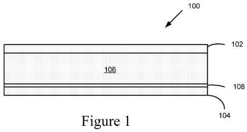
[0013] Figure 1 is a schematic illustration of an electro-optic device 100
according to an
embodiment of the current invention.
[0014] Figure 2 is a schematic illustration of an electro-optic device 200
according to another
embodiment of the current invention.
- 4 -
CA 02831394 2013-09-25
WO 2012/135527
PCT/US2012/031265
[0015] Figure 3 is a schematic illustration of an electro-optic device
according to an
embodiment of the current invention.
[0016] Figure 4 is a schematic illustration of an electro-optic device
according to another
embodiment of the current invention.
[0017] Figure 5 shows properties of a polymer according to one embodiment
of the
invention. Figure 5A shows UV-vis absorption spectrum of LT13. Figure 5B shows
electrochemical cyclic voltammetry spectrum of LT13.
[0018] Figure 6 shows I-V curve of a polymer solar cell according to one
embodiment of
the invention under simulated sunlight (AM 1.5, 100mW/crn-2) with a structure
of
ITO/PEDOT:PSS/LT13:PC70BM (1:2 wt/wt)/Ca/Al.
[0019] Figure 7 shows EQE curve of a polymer solar cell according to one
embodiment of
the invention with a structure of ITO/PEDOT:PSS/LT13:PC70BM (1:2 wt/wt)/Ca/A1.
The
devices efficiently harvest photons with wavelength from 300-900 nm.
[0020] Figure 8 shows I-V curve of a polymer tandem solar cell device
according to one
embodiment of th einvention under simulate sunlight (AM 1.5, 100mW/cm-2) with
a structure
of ITO/Ti02:Cs/P3HT:ICBA/PEDOT:PSS/Ti02:Cs/LT13:PC70BM/Ca/A1 (a) and
ITO/PEOT:PSS/ P3HT:ICBA/Ti02/LT13:PC70BM/Ca/A1 (b).
[0021] Figure 9 shows a polymer according to one embodiment of the
invention. Figure
9A shows the Chemical structure of PBDTT-DPP. Figure 9B shows UV-visible
absorption
spectra of PBDTT-DPP and P3HT film. The UV-visible absorption profiles of
PBDTT-DPP
and P3HT show that the two materials cover the solar spectrum from 350 to 850
nm
complementarily.
[0022] Figure 10 shows characteristics of single cell devices with regular
and inverted
structures. Figure 10A shows J-V characteristics of single cell devices with
regular and
inverted structures. Figure 10B shows EQE of the corresponding devices. Both
regular and
inverted single cell devices show identical performance with a Voc of 0.74 V,
Jsc of ¨14
mA/cm2, FF of ¨65% and PCE of about 7%. The devices exhibit a very broad
response range
covering 350 nm to 850 nm.
[0023] Figure 11 shows an embodiment of the invention using electron
acceptors. Figure
11A shows chemical structures of P3HT, IC60BA and PC71BM. Figure 11B shows
device
structure of an inverted tandem solar cell. Figure 11C shows the energy
diagram of inverted
- 5 -
CA 02831394 2013-09-25
WO 2012/135527
PCT/US2012/031265
tandem devices. Figure 11D shows J-V characterstics of an inverted tandem
solar cell.
Figure 11E shows stability of inverted front cells, rear cells and tandem
cells.
[0024] Figure 12 shows electrochemical cyclic voltammogram of PBDT-DPP and
PBDTT-DPP.
[0025] Figure 13 shows ./5¨V plots for the polymer film using SCLC model
with device
structure of ITO/PEDOT:PSS/Polymer/Au.
[0026] Figure 14 shows X-ray diffraction profiles of PBDTT-DPP and PBDT-DPP.
[0027] Figure 15 shows AFM phase images of PBDTT-DPP:PC71BM based single cell
devices under different treatments. Figure 15A shows AFM phase images after no
further
treatment. Figure 15B shows AFM phase images after treatment with 2% DIO in
dichlorobenzene. Figure 15C shows AFM phase images after annealing at 110 C
for 15
min. Figure 15D shows AFM phase images after solvent annealing.
[0028] Figure 16 shows current density¨voltage (J¨V) characteristics of
PBDTT-
DPP:PC7IBM based polymer solar cell with a structure of ITO/PEDOT:PSS/PBD'TT-
DPP:
PC7IBM/Ca/A1 with no further treatment, after treatment with 2% DIO in
dichlorobenzene,
after annealing at 110 C for 15 min, and after solvent annealing.
DETAILED DESCRIPTION
[0029] In describing embodiments of the present invention, specific
terminology is employed
for the sake of clarity. However, the invention is not intended to be limited
to the specific
terminology so selected. It is to be understood that each specific element
includes all
technical equivalents which operate in a similar manner to accomplish a
similar purpose. The
broad concepts of the current invention should not be construed as being
limited to the
specific examples.
Definitions and Nomenclature
[0030] Unless otherwise indicated, this invention is not limited to
specific starting
materials, regents or reaction conditions, as such may vary.
[0031] The term "alkyl" as used herein refers to a branched or unbranched
saturated
hydrocarbon group typically although not necessarily containing 1 to 18 carbon
atoms, 4 to 18
carbon atoms, or 6 to 12 carbon atoms, such as methyl, ethyl, n-propyl,
isopropyl, n-octyl, 2-
- 6 -
CA 02831394 2013-09-25
WO 2012/135527
PCT/US2012/031265
ethylhexyl, 2-butyloctyl, isooctyl, decyl, and the like, as well as cycloalkyl
groups such as
cyclopentyl, cyclohexyl and the like.
[0032] The terms "aryl" and "arylene" as used herein refer to an aromatic
hydrocarbon ring
system. Aryl or arylene groups may be monocyclic, bicyclic or polycyclic.
Monocyclic aryl or
arylene has a single aromatic ring. Bicyclic aryl or arylene rings have two
fused rings.
Polycyclic aryl or arylene has more than two fused rings and may have 3, 4, 5,
6, or more
fused rings.
[0033] The term "heteroarylene" as used herein refers to a hydrocarbon
arylene in which
one or more carbon atoms are replaced with a "heteroatom" other than carbon,
e.g., nitrogen,
oxygen, sulfur, silicon, selenium, phosphorus.
[0034] The term "substituted" as in "substituted aryl," "substituted
arylene", "substituted
heteroarylene", and the like, is meant that in the arylene or heteroarylene,
or other moiety, at
leaset one hydrogen atom bound to a carbon (or other) atom is replaced with
one or more
non-hydrogen substituents. Such substituents include, but not limited to,
functional groups
such as alkyl (as defined herein), halo (fluoro, chloro, bromo, or iodo),
haloalkyl (alkyl, as
defined herein, substituted with one or more F, CI, Br, or I atom, such as,
for example,
trifluoromethyl), hydroxyl, alkylthio, alkoxy, aryloxy, alkylcarbonyl,
acyloxy, nitro, cyano,
and the like.
[0035] Figure 1 and Figure 3 are schematic illustrations of single-layer
electro-optic devices
according to some embodiments of the current invention.
Tandem Photovoltaic Devices
[0036] Some embodiments of the current invention include tandem polymer
photovoltaic
devices having a hole extracting electrode and an electron extracting
electrode spaced apart
from the hole extracting electrode. The tandem polymer photovoltaic device
further includes
a first bulk hetero-junction polymer semiconductor layer and a second bulk
hetero-junction
polymer semiconductor layer spaced apart from said first bulk hetero-junction
polymer
semiconductor layer.
[0037] Between the first and second bulk hetero-junction polymer
semiconductor layers,
the tandem photovoltaic device further includes a p-type layer in physical
contact with one of
the first and second bulk hetero-junction polymer semicondutor layers, and an
n-type layer in
- 7 -
CA 02831394 2013-09-25
WO 2012/135527
PCT/US2012/031265
physical contact with the other of the first and second bulk hetero-junction
polymer
semiconductor layer where at least one of the p-type layer and the n-type
layer is doped to an
extent that charge carriers tunnel through the p-type and/or n-type layer.
[0038] As used herein, the first bulk hetero-junction polymer semiconductor
layer and
second bulk hetero-junction polymer semiconductor layer may be refered to as
"active
layers."
[0039] Figure 2 is a schematic illustration of a tandem electro-optic
device 200 according
to an embodiment of the current invention. The electro-optic device 200 has a
first electrode
202, a second electrode 204 spaced apart from the first electrode 202, and an
active layer 206
disposed between the first electrode and the second electrode. This embodiment
is an
example of a tandem electro-optic device that has a second active layer 210
between the first
electrode 202 and the second electrode 204. The electro-optic device 200 also
includes a
region 208, between the two active layers 206 and 210, having a p-type layer
in physical
contact with one of the first and second bulk hetero-junction polymer
semicondutor layers,
and an n-type layer in physical contact with the other of the first and second
bulk hetero-
junction polymer semiconductor layer. Devices according to the current
invention are not
limited to only one or two active layers; they may have multiple active layers
in some
embodiments of the current invention.
[0040] Figure 4 is a schematic illustration of tandem polymer solar cell
device according
to another embodiment of the current invention. Figure 4 shows a device with
multiple active
layers. For example, a tandem photovoltaic cell that has two or more active
layers with thin
interfacial layers. Figure 4A is an inverted structure and Figure 4B is a
conventional
structure for a tandem solar cell. The schematic illustrations of Figures 2
and 4 are shown as
examples. Devices according to other embodiments of the current invention are
not limited to
these specific examples.
[0041] Physical contact, as used here, means that the two layers are
directly adjacent to
each other, without an intervening layer.
[0042] A charge carrier may be either an electron or hole, depending on the
type of layer.
In a p-type layer, the charge carrier is a hole. In an n-type layer, the
charge carrier is an
electron.
[0043] The p-type layer and n-type layer between the two active layers
promote tunneling
- 8 -
CA 02831394 2013-09-25
WO 2012/135527
PCT/US2012/031265
of electrons and holes across the layers without significant loss of voltage
across the device.
This is achieved by doping at least one of the n-type layer and p-type such
that the related
charge carriers tunnel through the layer. In tandem devices according to some
embodiments
of the invention, charge carriers tunnel through the p-type and/or n-type
layer and then
recombination occurs. For example, in an inverted tandem device, only
electrons generated in
the active layer closest to the transparent electrode and holes generated in
the active layer
further from the transparent electrode can be extracted by the electrodes. The
holes generated
by the front cell and electrons generated by the rear cell will recombine
after tunnelling
through either the p-type and/or n-type layer. Doping the n-type and/or p-type
layer makes
the tunneling easier and may enhance conductivity.
[0044] Charge carrier tunneling depends on the material used to form the
layer and the
type of dopant, for example. If charge carrier tunneling does not occur at a
particular
concentration of dopant in a particular material, more dopant may be added to
induce
tunneling in that layer. Similarly, if doping only one of the n-type layer and
p-type layer is
insufficient to create carrier tunneling, both the n-type layer and p-type
layer may be doped.
[0045] As used herein, a hole extracting electrode is an electrode where
holes produced by
the photovoltaic active layer are extracted from the device. A hole extracting
electrode may
be a single layer electrode or composite electrode, and may be composed of,
for example,
silver (Ag), or aluminum (AI). Examples of materials used in single layer
electrode include
those with high work function (>4eV) such as Al, Ag, Au, Pt, ITO, graphene,
graphite, and
cotnbinations thereof. Composite electrodes may include, for example, a metal
electrode with
p-type interface layer such as PEDOT:PSS, PANI, Mo0x, V205, V0x, W03, W0x,
NiO,
Ni0x, grapheme oxide, or any combination of the above.
[0046] As used herein, an electron extracting electrode is an electrode
where electrons
produced by the photovoltaic active layer are extracted from the device. An
electron
extracting electrode may be a single layer electrode or a composite electrode.
The electron
extracting electrode may be composed of, for example, Indium-tin-oxide (ITO).
The
electron-extracing electrode may be, for example, a low work function metal
such as, for
example, Ca, Ba, Mg, Mg:Ag alloy, combined with stable electrode such as Al,
Ag, ITO, Au
or combinations thereof. Composite electron-extracting electrodes include, for
example,
metal electrode (such as Al, Ag, Au, Pt, ITO, graphene, graphite, combination
of them),
- 9 -
CA 02831394 2013-09-25
WO 2012/135527
PCT/US2012/031265
combined with n-type interface layer such as metal oxide (ZnO, ZnOx, Ti02,
TiOx), salts
(Cs2CO3, LiF, CsF etc.), polyelectrolyte, and the combination of two or more
of the above.
[0047] In some embodiments, at least one of the electrodes is transparent.
In some
embodiments, the electron-extracting electrode is transparent.
[0048] In some embodiments, one of the two electrodes is formed on a
substrate, and the
other layers added one at a time on the first electrode. In some embodiments,
the electron-
extracting electrode may be on a transparent substrate, and the device
fabricated on the
electron-extracting electrode. For example, the electron-extracting electrode
may be Indium-
tin-oxide (ITO) on a transparent glass substrate.
[0049] As used herein, a bulk hetero-junction polymer semiconductor layer
includes a
blend of a photoactive polymer and admixer. The combination of polymer and
admixer are
selected such that charge and/or energy transfer takes place between the
admixer and the
polymer when an excitation source, including light or voltage, is applied.
[0050] Some embodiments include devices with more than two bulk hetero-
junction
polymer semiconductor layers. Any additional bulk hetero-junction polymer
semiconductor
layers may be separated from the first or second bulk hetero-junction polymer
semiconductor
layer by a p-type/n-type layer as described herein, may include another type
of interlayer, or
use no interlayer.
[0051] Some embodiments include an "inverted" tandem structure. In an
inverted tandem
device as used herein, the p-type layer between the two active layers is
closer to the electron-
extracting electrode than the n-type layer. In some embodiments of an inverted
tandem
structure, the electron-extracting electrode is transparent. Some embodiments
of an inverted
tandem device further include an electron transporting layer (of an n-type
material) adjacent
to the electron-extracting electrode.
[0052] In some embodiments, the p-type layer is in physical contact with
the n-type layer.
In other words, in these embodiments, there is no additional layer between the
p-type layer
and the n-type layer.
[0053] The p-type layer may be composed of any p-type semiconducting
material, so long
as when the p-type layer is doped the p-type semiconducting material is
compatible with the
dopant and holes tunnel through the doped p-type layer. The p-type
semiconducting material
may be organic or inorganic. Examples of organic p-type materials include, for
example,
-10-
CA 02831394 2013-09-25
WO 2012/135527
PCT/US2012/031265
poly(3,4-ethylenedioxythiophene) (PEDOT), poly(aniline) (PANT) or other p-type
organic
material. Examples of inorganic p-type material include, for example, Mo03,
Mo0x, V205,
V0x, W03, W0x, NiO, Ni0x, graphene oxide, or any combination of the above. In
some
embodiments, the p-type layer include a p-type polymer, such as, for example,
poly(3,4-
ethylenedioxythiophene) (PEDOT). In some embodiments, the p-type layer
includes a p-type
metal oxide, such as, for example, Mo0x, Mo03, or V205.
[0054] In some embodiments, the p-type layer is doped to an extent that
holes tunnel
through the doped p-type layer. In principle, any p-type dopant may be used in
the p-type
layer, so long as it is compatible with the p-type material forming the layer.
Examples of p-
type dopants for organic p-type layers, include, for example, acid, such as
poly(styrenesulphonic acid), H202, or other p-type dopant. Examples of p-type
dopants for
inorganic (including p-type metal oxide) p-type layers include, for example
FeC13, 12, H202.
As will be apparent to one of ordinary skill, some dopants may be used with
organic or
inorganic p-type materials.
[0055] The n-type layer may be composed of any n-type semiconducting
material, so long
as when the n-type layer is doped, the n-type semiconducting material is
compatible with the
dopant and electrons tunnel through the doped n-type layer. The n-type
semiconducting
material may be organic or inorganic material. Examples of organic n-type
materials include,
for example, polyelectrolyte, small molecules (such as, for example,
bathocuproine, 3-
(Bipheny1-4-y1)-5-(4-tert-butylpheny1)-4-phenyl-411-1,2,4-triazole, 2-(4-
Biphenyly1)-5-
pheny1-1,3,4-oxadiazole, Bis(8-hydroxy-2-methylquinoline)-(4-
phenylphenoxy)aluminum,
Tris-(8-hydroxyquinoline) aluminum, among others), graphene, graphite.
Examples of
inorganic n-type materials include, for example, metal oxides (e.g. ZnO, ZnOx,
Ti02, TiOx),
salts (e.g. Cs2CO3, LiF, CsF etc.), and the combination of two or more of
them. In some
embodiments, the n-type layer is an n-type metal oxide, such as, for example,
ZnO or Ti02.
In some embodiments, the n-type layer includes ZnO.
[0056] In some embodiments, the n-type layer is doped to an extent that
electrons tunnel
through the n-type layer. In principle, any n-type dopant may be used in the n-
type layer, so
long as it is compatible with the n-type material forming the layer. Examples
of n-type
dopants for organic n-type layers include, for example low work function
metals such as Na,
Li, Al, low work function fluorides such as LiF, CsF, low work function salts
such as
- 11 -
CA 02831394 2013-09-25
WO 2012/135527
PCT/US2012/031265
Cs2CO3. Examples of n-type dopants for inorganic n-type layers include, for
example low
work function metals such as Na, Li, Al, low work function fluorides such as
LiF, CsF, low
work function salts such as Cs2CO3. As will be apparent to one of ordinary
skill, some n-
type dopants may be used with both organic and inorganic n-type materials.
[0057] In some embodiments, both the p-type layer and said n-type layer are
doped, so
long as the charge carriers tunnel through the layers. The same dopants
described above for
use in individual p-type or n-type layers may be used.
[0058] In some embodiments, the device further includes an electron
transporting layer. In
some embodiments, such as inverted tandem devices, the electron transporting
layer may be
between the electron-extracting electrode and the first bulk hetero-junction
polymer
semiconductor layer or second bulk hetero-junction polymer semiconductor
layer, whichever
is closest to the electron extracting electrode. In some embodiments of tandem
devices, the
electron transporting layer may be between the hole-extracting electrode and
the first bulk
hetero-junction polymer semiconductor layer or second bulk hetero-junction
polymer
semiconductor layer, whichever is closest to the hole-extracting electrode.
Any n-type
material may be used in the electron transporting layer, including those
described for the n-
type layer between the two active layers. In some embodiment, the material in
the electron
transporting layer may be the same as or different than the material used in
the n-type layer
between the two active layers. The electron transporting layer may be, but
need not be,
doped. In some embodiments, the electron transporting layer may be, for
example, an n-type
metal oxide, such as, for example ZnO.
[0059] In some embodiments, the tandem polymer photovoltaic device further
includes a
hole transporting layer. In some embodiments, such as inverted tandem devices,
the hole
transporting layer may be between the hole-extracting electrode and the first
bulk hetero-
junction polymer semiconductor layer or second bulk hetero-junction polymer
semiconductor
layer, whichever is closest to the hole extracting electrode. In some
embodiments of tandem
devices, the hole transporting layer may be between the electron-extracting
electrode and the
first bulk hetero-junction polymer semiconductor layer or second bulk hetero-
junction
polymer semiconductor layer, whichever is closest to the electron-extracting
electrode. Any
p-type material may be used in the hole transporting layer, including those
described for the
p-type layer between the two active layers. The material in the hole
transporting layer may be
- 12 -
CA 02831394 2013-09-25
WO 2012/135527
PCT/US2012/031265
the same as or different than the material used in the p-type layer between
the two active
layers. The hole transporting layer may be, but need not be, doped. In some
embodiments,
the electron transporting layer may be, for example, a p-type organic
material, such as, for
example, PEDOT-PSS, or a p-type metal oxide, such as, for example Mo03 or
V205.
[0060] In some embodiments, the first bulk hetero-junction polymer
semiconductor layer
is closer to the transparent electrode than the second bulk hetero-junction
polymer
semiconductor layer. In some embodiments where the transparent electrode is
the electron
extracting electrode, the first bulk hetero-junction polymer semiconductor
layer is closer to
the electron extracting electrode.
[0061] Any two photoactive polymers may be used in the tandem photovoltaic
device
described herein. However, it may be advantageous for one polymer to have a
wider bandgap
and one polymer to have a narrower bandgap. Of the two photoactive polymers,
the polymer
with the wider bandgap may be described as a high bandgap polymer, while the
polymer with
the narrower bandgap may be described as a low bandgap polymer.
[0062] In some embodiments, the high bandgap polymer may have a bandgap
greater than
about 1.6, greater than about 1.7, greater than about 1.8, greater than about
1.9, or greater than
about 2.0 eV. Examples of high bandgap polymers that may be used include
poly(3-
hexylthiophene) (P3HT) or other polymer materials, such as, for example,
derivatives of
poly(p-phenylene vinylene), such as MEH-PPV and MDMO-PPV, and some derivatives
of
poly(3-alky-thiophene), such as P3HT and P3OT. Specific examples include,
poly(3-
hexylthiophene) (P3HT), Poly[[9-(1-octylnony1)-9H-carbazole-2,7-diy1]-2,5-
thiophenediy1-
2,1,3-benzothiadiazole-4,7-diy1-2,5-thiophenediy1], poly[4,8-bis((2-
ethylhexyl)oxy)benzo[1,2-b:4,5-bldithiophene-2,6-diyhalt-5-(2-ethylhexyl)-4H-
thieno[3,4-
c]pyrrole-4,6(5H)-dione-1,3-diy1] (PBDT-TPD), poly[(4,4'-bis(2 -
ethylhexyl)dithieno[3,2-
b:2',3'-d]silole)-2,6-diyl-alt-5-(2-ethylhexyl)-4H-thieno[3,4-c]pynole-4,6(5H)-
dione-1,3-diy1]
(PDTS-TPD), ), poly[(4,4'-bis(2 -ethylhexyl)dithieno[3,2-b:2',31-d]germole)-
2,6-diyl-alt-5-(2-
ethylhexyl)-4H-thieno[3,4-c]pyffole-4,6(5H)-dione-1,3-diy1] (PDGS-TPS),
poly[4,8-(3-
hexylundecyl)benzo[1,2-b:4,5-bldithiophene-2,6-diyl-alt-4,7-bisthiophen-2-y1-2-
(2-
butylocty1)-5,6-difluoro-2H-benzo[d] [1,2,3]triazole-5,5' -diy1] (PBnDT-FTAZ).
Poly
benzodithiophen-alt-thienothiophene (PTB series, BG ¨1.6eV) can also be used
as high
bandgap polymer.
- 13 -
CA 02831394 2013-09-25
WO 2012/135527
PCT/US2012/031265
[0063] In some embodiments, the low bandgap polymer has a bandgap of less
than about
1.9 eV, less than about 1.8 eV or less than about 1.7 eV, so long as the low
bandgap polymer
has a lower bandgap than the high bandgap polymer. Examples of low bandgap
polymers
that may be used include the conjugated polymers described herein, or other
low bandgap
polymers, such as, for example, poly[4,8-bis-substituted-benzo[1,2-b:4,5-
13']dithiophene-2,6-
diyl-alt-4-substituted-thieno[3, 4-b]thiophene-2,6-diy1] (PBDT'TT), poly{2,6'-
4,8-di(5-
ethylhexylthienyl)benzo[1,2-b;3,4-b]dithiophene-alt-5-dibutylocty1-3,6-bis(5-
bromothiophen-
2-yOpyrrolo[3,4-c]pyrrole-1,4-dionel(PBDTT-DPP), poly[2,6-(4,4-bis-(2-
ethylhexyl)-4H-
cyclopenta[2,1-b;3,4-bldithiophene)-alt-4,7-(2,1,3-benzothiadiazole)]
(PCPDTBT),
poly[(4,4'-bis(2 -ethylhexyl)dithieno[3,2-b:2',3'-d]silole)-2,6-diyl-alt-
(2,1,3-
benzothiadiazole)-4,7-diy1] (PSBTBT), poly[3,6-bis(4'-dodecyl[2,21-bithiophen]-
5-y1)-2,5-
bis(2-hexyldecy1)-2,5-dihydro-pyrrolo[3,4-c]pyrrole-1,4-dione-alt-thiophene-
2,5-diy1]
(PDPP5T). In some embodiments, the polymers described herein may be used as
the low
bandgap polymer.
[0064] In some embodiments, the polymer used in the first bulk hetero-
junction polymer
semiconductor layer has a wider bandgap than the polymer used in the second
bulk hetero-
junction polymer semiconductor layer. In some of these embodiments, the first
bulk hetero-
junction polymer semiconductor layer is closer to the transparent electrode.
Thus, light
passing through the transparent electrode passes first through the bulk hetero-
junction
polymer semiconductor layer having a polymer with a wider bandgap, and then
through the
bulk hetero-junction polymer semiconductor layer having a polymer with a
narrower
bandgap.
[0065] The absorbance in the region between about 300 nm and about 1000 nm of
the two
polymers used in the first and second bulk hetero-junction polymer
semiconductor layers
affects the performance of the device. In some embodiments, to improve
performance, the
absorbance spectra of the two polymers in the region between about 300 nm and
about 1000
nm may be separated, though some overlap between the absorbance spectra of the
two
polymers may be acceptable to absorb light across a broad range of
wavelengths.
[0066] In some embodiments, the separation between absorbance spectra of
the two
polymers may be determined by the wavelength where each polymer has maximum
absorbance. In these embodiments, the polymer used in the first bulk hetero-
junction polymer
- 14 -
CA 02831394 2013-09-25
WO 2012/135527
PCT/US2012/031265
semiconductor layer may have an absorbance maximum between about 400 nm and
about
700 nm and the polymer used in the second bulk hetero-junction polymer
semiconductor layer
as an absorbance maximum between 700 nm and about 1000 nm.
[0067] In some embodiments, the wavelength of maximum absorbance (absorbance
maximum) of the polymer used in the first bulk hetero-junction polymer
semiconductor layer
is more than 20 nm, more than 30 nm, more than 40 nm, more than 50nm, more
than 75nm,
more than 100 nm, more than 125nm, more than 150 nm, more than 175nm, more
than 200
nm, more than 225nm, or more than 250 nm shorter than the absorbance maximum
of the
polymer used in the second bulk hetero-junction polymer semiconductor layer.
In other
words, the wavelength where the first polymer has maximum absorbance should be
shorter by
some degree than the wavelength where the second polymer has maximum
absorbance.
[0068] In some embodiments, the wavelength of the trailing edge at 10%,
15%, 20%,
25%, 30%, 35%, 40%, 45%, 50%, 55%, or 60% of the maximum absorbance of the
absorbance spectrum between 300nm and 1000nm of the polymer used in the first
bulk
hetero-junction polymer semiconductor layer is shorter than or equal to the
wavelength of the
leading edge at 10%, 15% 20%, 25%, 30%, 35%, 40%, 45%, 50%, 55%, or 60% of the
maximum absorbance the absorbance spectrum between 300nm and 1000nm of the
polymer
used in the second bulk hetero-junction polymer semiconductor layer. To make
this
comparison the wavelength of absorbance of the first polymer should be
measured at the
trailing edge of the absorbance spectrum between 300nm and 1000nm at the point
10%, 15%,
20%, 25%, 30%, 35%, 40%, 45%, 50%, 55%, or 60% of the maximum absorbance
intensity
(i.e. at the point where the height of the absorbance spectrum is 10%, 15%,
20%, 25%, 30%,
35%, 40%, 45%, 50%, 55%, or 60% of the height of the absorbance spectrum at
the
absorbance maximum). The wavelength of absorbance of the second polymer should
be
measured at the leading edge of the absorbance spectrum at the point 10%, 15%,
20%, 25%,
30%, 35%, 40%, 45%, 50%, 55%, or 60% of the maximum absorbance intensity (i.e.
at the
point where the height of the absorbance spectrum is 10%, 15%, 20%, 25%, 30%,
35%, 40%,
45%, 5.0i,
u /0 55%, or 60% of the height of the absorbance spectrum at the absorbance
maximum). The value determined for the first polymer should be shorter than or
equal to the
value determined for the second polymer.
[0069] In some embodiments, the absorbance at the wavelength halfway
between the
- 15 -
CA 02831394 2013-09-25
WO 2012/135527
PCT/US2012/031265
absorbance maximum of the polymer used in the first bulk hetero-junction
polymer
semiconductor layer and the absorbance maximum of the polymer used in the
second bulk
hetero-junction polymer semiconductor layer in the sum of the normalized
absorbance spectra
measured between 300nm and 1000nm is greater than 50%, greater than 45%,
greater than
40%, greater than 35%, greater than 30%, greater than 25%, greater than 20%,
greater than
15%, or greater than 10% of the normalized maximum absorbance of either
polymer
individually. In some embodiments, the absorbance at the wavelength halfway
between the
absorbance maximum of the polymer used in the first bulk hetero-junction
polymer
semiconductor layer and the absorbance maximum of the polymer used in the
second bulk
hetero-junction polymer semiconductor layer in the sum of the normalized
absorbance spectra
is less than 150%, less than 140%, less than 130%, less than 120%, less than
110%, less than
100%, or less than 90% of the normalized maximum absorbance of either polymer
individually. To measure this, the absorbance spectrum of each polymer should
be measured,
the wavelength of maximum absorbance of each polymer determined and each
absorbance
spectrum normalized so that each has the same maximum absorbance intensity at
the
wavelength of maximum absorbance for each polymer. For example, if the
absorbance of the
first polymer at its maximum absorbance wavelength is 1.0, the absorbance
spectrum of the
second polymer should be adjusted so that the absorbance at the maximum
absorbance of the
second polymer is also 1Ø The two normalized spectra, measured between about
300 nm
and about 1000 nm should then be added together to produce a combined spectrum
(a sum of
the normalized spectra). At the wavelength halfway between the absorbance
maximum of the
first polymer and the absorbance maximum of the second polymer, the absorbance
of the
combined spectrum may be greater than 50%, greater than 45%, greater than 40%,
greater
than 35%, greater than 30%, greater than 25%, greater than 20%, greater than
15%, or greater
than 10% of the normalized absorbance of the individual polymers at their
absorbance
maximum. Likewise, At the wavelength halfway between the absorbance maximum of
the
first polymer and the absorbance maximum of the second polymer, the absorbance
of the
combined spectrum may be less than 150%, less than 140%, less than 130%, less
than 120%,
less than 110%, less than 100%, or less than 90% of the normalized absorbance
of the
individual polymers at their absorbance maximum. For example, where the
absorbance
spectra of the first polymer and second polymer have been normalized so that
each has an
absorbance of 1.0 at the absorbance maximum, where the first polymer has an
absorbance
- 16 -
CA 02831394 2013-09-25
WO 2012/135527
PCT/US2012/031265
maximum at 500nm, and the second polymer has an absorbance maximum at 800nm.
The
absorbance at 650nm of the addition spectrum may be greater than 50%, greater
than 45%,
greater than 40%, greater than 35%, greater than 30%, greater than 25%,
greater than 20%,
greater than 15%, or greater than 10% of the normalized absorbance of the
absorbance at
500nm and 800 nm. The absorbance at 650nm of the addition spectrum may be less
than
150%, less than 140%, less than 130%, less than 120%, less than 110%, less
than 100%, or
less than 90% of the absorbance at 500nm and 800 nm.
[0070] In some embodiments, the electron extracting electrode is a
transparent electrode,
and the first bulk hetero-junction polymer semiconductor layer is closer to
the transparent
electrode than the second bulk hetero-junction polymer semiconductor layer.
The p-type layer
between the two active layers is closer to the electron extracting electrode,
creating an
inverted tandem device.
[0071] Figure 11B shows a schematic illustration of an example embodiment
of an
inverted tandem device having a transparent electron extracting electrode of
indium-tin-oxide
(ITO), and a hole extracting electrode of silver (Ag). The first bulk hetero-
junction polymer
semiconductor layer is closer to the transparent electrode, and includes a
high bandgap
polymer P3HT blended with admixer ICBA. The second bulk hetero-junction
polymer
semiconductor layer includes a low bandgap polymer PBDTT-DPP (a polymer
described in
detail below) and admixer PC7IBM. Between the active layers is a p-type layer
closer to the
transparent electrode made of PEDOT doped with PS S, and an n-type layer of
ZnO.
[0072] The example device in Figure 11B also includes an electron
transporting layer of
ZnO between first bulk hetero-junction polymer semiconductor layer and the
electron
extracting electrode. The example device in Figure 11B also includes a hole
transporting
layer of Mo03 between the second bulk hetero-junction polymer semiconductor
layer and the
hole extracting electrode. The schematic illustration in Figure 11B is shown
as an example.
Devices according to other embodiments of the current invention are not
limited to this
specific example.
Polymers
[0073] Conjugated polymer materials for polymer solar cell should have high
mobility, so the
main chains of the conjugated polymers should have a planar structure
according to some
- 17 -
CA 02831394 2013-09-25
WO 2012/135527
PCT/US2012/031265
embodiments of the current invention. This can also be helpful to form 7C-7C
stacking
structures and facilitate charge transfer between two adjacent main chains.
Some materials
should have a low band gap to provide good harvesting of sunlight; they also
should have
proper molecular energy levels that match with electrode and electron acceptor
materials in
polymer solar cell devices. It thus would be desirable according to some
embodiments of the
current invention to provide conjugated polymers as photovoltaic materials
that possess some
or all of the properties mentioned above.
[0074] Some embodiments of the invention include polymers having repeated
units of the
general structure of formula (I)
Ii R3
I 0 /
*
R2 Ari N
Ar2¨...:
X
7 0 n
Ari R2 R3
I
Ri (I)
where RI, R2, and R3 are independently selected from alkyl groups with up to
18 C atoms,
aryls and substituted aryls. X is selected from Oxygen, Sulfur, Selenium and
Nitrogen atoms.
[0075] Art and Ar2 may be each, independently, one to five monocyclic
arylene, bicyclic
arylene, polycyclic arylene, monocyclic heteroarylene, bicyclic heteroarylene
or polycyclic
heteroarylene groups, either fused or linked. As used here, "fused" means that
the one to five
arylene or heteroarylene groups are fused into a single polycyclic moiety. As
used here,
"linked" means that the one to five arylene or heteroarylene groups are linked
in a series of
repeated arylene or heteroarylene moieties.
[0076] In some embodiments, Art and Ar2 are the same. In some embodiments MI
and
Ar2 are different.
[0077] In principle, Ari may be any substituted or unsubstituted arylene or
heteroarylene
group, so long as it contains one available position to connect to the polymer
chain, and one
position having a substitutent R1 or available to incorporate a substituent
RI. In principle, Ar2
may be any substituted or unsubstituted arylene or heteroarylene group so long
as it contains
two available positions for incorporation into the polymer backbone.
[0078] In some embodiments, Ari and Ar2 may be, independently, a 5-membered
heteroarylene ring. In some embodiments, An and Ar2 may be, independently, two
linked 5-
- 18 -
CA 02831394 2013-09-25
WO
2012/135527 PCT/US2012/031265
membered heteroarylene rings. In some embodiments, Ari and Ar2 may be,
independently, a
6-membered arylene or heteroarylene ring. In some embodiments, Ari and Ar2 may
be,
independently, a 6-membered arylene or heteroarylene ring fused to a 5-
membered
heteroarylene ring. In some embodiments, Ari and Ar2 may be, independently, a
6-membered
arylene or heteroarylene ring fused to a 6-membered arylene or heteroarylene
ring. In some
embodiments, Ari and Ar2 may be, independently, a 5-membered heteroarylene
ring fused to
a 5-membered heteroarylene ring. In some embodiments, Ari and Ar2 may be,
independently, three fused 6-membered arylene or heteroarylene rings. In some
embodiments, Ari and Ar2 may be, independently, two fused 6-membered arylene
or
heteroarylene rings fused to a 5-membered heteroarylene ring. In some
embodiments, An
and Ar2 may be, independently, a 6-membered arylene or heteroarylene ring
fused to two 5-
membered heteroarylene rings.
[0079] In some embodiments, Ari and Ar2 may be, independently, a
substituted or
unsubstituted arylene hydrocarbon. In some embodiments, Ari and Ar2 may be,
independently, a heteroarylene group containing 1, 2, 3, or 4 nitrogen atoms.
In some
embodiments, Ari and Ar2 may be, independently, a heteroarylene group
containing 1, 2, 3, or
4 sulfur atoms. In some embodiments, An and Ar2 may be a heteroarylene group
containing
at least one (e.g. 1, 2, 3, 4, or more) oxygen atom. In some embodiments, Ari
and Ar2 may be
a heteroarylene group containing at least one (e.g. 1, 2, 3, 4 or more)
nitrogen atom and at
least one (e.g. 1, 2, 3, 4 or more) sulfur atom. In some embodiments, An and
Ar2 may be a
heteroarylene group containing at least one (e.g. 1, 2, 3, 4, or more)
nitrogen atom and at least
one (e.g. 1, 2, 3, or 4) oxygen atom. In some embodiments, Ari and Ar2 may be
a
heteroarylene group containing at least one (e.g. 1, 2, 3, 4, or more)
selenium atom. In some
embodiments, Ari and Ar2 may be a heteroarylene group containing at least one
(e.g. 1, 2, 3,
4, or more) nitrogen atom and at least one (e.g. 1, 2, 3, 4, or more) selenium
atom.
[0080] Examples of suitable Ari and Ar2 moieties include, but are not
limited to, the
following:
R R R R R R
0 Se Se
R R
N-N N-N N-N N=N
0
R R
- 19 -
CA 02831394 2013-09-25
WO 2012/135527
PCT/US2012/031265
/--- N j¨ /-=-
%_N ---N=N N=N (\ _12¨ '--- ----
N N N N-N
R R
R
/S ----N R / s N'S
---- 1 '>---
-4S)\--- N----S /
R S S
R R R R R R R R
410 410 4110 RtN\)-- tN\h- ---eN1,--
ii
N,seN
N,S,N N,0,N N,SeN N,S, N N,0,N
R R R R R R
1
410
It NI \ N
N=N N=N N N
N/ \ N =410 N----N
N " N
Al ili 111 411
N " hi 41
NN NN
RRRR RRRR R RR R
S S 0 0 Se Se
[0081] In the above structures, R is proton or fluorine atom or CF3 or CN
or NO2 or alkyl
group with carbon atom number of 1-18.
[0082] Some embodiments of polymers of formula (I) are have repeated units
where RI,
R2, and R3 are alkyl groups with carbon atom number of 4-18, X is selected
from Oxygen,
Sulfur, Selenium and Nitrogen atoms, and Ari and Ar2 may be, independently:
R R R R R R
N-N N-N
R R R
S S N N=N
\ I \ ---N I .
S S
R R R
¨D N=N --i ---
N-N
where R is a proton or fluorine atom or CF3 or CN or NO2 or alkyl group with
carbon atom
number of 1-18. In some embodiments, one of Ari and Ar2 is thiophene. In some
embodiments, both An and Ar2 are thiophene.
[0083] In some embodiments, the polymer of formula (I) has repeated units
of formula
(II), where R1 and R3 are alkyl groups with carbon atom number of 6-12, R2 is
proton, Ari and
- 20 -
CA 02831394 2013-09-25
WO 2012/135527
PCT/US2012/031265
Ar2 are thiophene, and X is sulfur.
R1 _ R3
s.- n /
w N s *
* 1 * Si
/ \ /
S S N 0
/ S 1
3 n
¨
R1 OD
[0084] The number average molecular weight of the polymer may be in the range
of about
1000 to about 1,000,000 for some embodiments, with some embodiments having a
number
average molecular weight in the range of about 5000 to about 500,000, and
further
embodiments having a number average molecular weight in the range of about
20,000 to
about 200,000. It will be appreciated that molecular weight can be varied to
optimize polymer
properties. For example, lower molecular weight is preferred to ensure
solubility, while a
higher molecular weight is preferred to ensure good film-forming property.
Polymer Preparation
[0085] The polymers of the invention can be generally synthesized by co-
polymerizing
monomers having the structure of formula (III) and formula (IV),
R1
I
R2 A I)
X 0 1,
Y / / Y
X
Z¨Ar2 /
Ari R2 N
/ o
I ..
R1 (III) , (IV)
[0086] where RI, R2, R3, Ai), Ar2 and X are as defined above; Y is
dependently selected
on Z. If Y is selected from boronic acid group, or boric acid esters groups
including, but not
being limited to, 1,3,2-dioxaborinane-2-yl, 4,4,5,5-tetramethyl- 1,3,2-
dioxaborolane-2-yl, and
5,5-dimethy1-1,3,2-dioxaborinane-2-yl, or magnesium halide groups including
magnesium
chloride, magnesium bromide, and magnesium iodide, or zinkhalide groups
including
zinkchloride and zinkbromide, or trialkyltin groups including, but not being
limited to,
trimethyl tin, triethyl tin, and tributyl tin, Z should be selected from I,
Br, or CI, and if Y is
selected from I, Br, or CI, Z should be selected from boronic acid group, or
boric acid esters
groups including, but not being limited to, 1,3,2-dioxaborinane-2-yl, 4,4,5,5-
tetramethyl-
- 21 -
CA 02831394 2013-09-25
WO 2012/135527
PCT/US2012/031265
1,3,2-dioxaborolane-2-yl, and 5,5-dimethy1-1,3,2-dioxaborinane-2-yl, or
magnesium halide
groups including magnesium chloride, magnesium bromide, and magnesium iodide,
or
zinkhalide groups including zinkchloride and zinkbromide, or trialkyltin
groups including,
but not being limited to, trimethyl tin, triethyl tin, and tributyl tin.
[0087] A polymerization route of the polymers in the patent using monomers
as mentioned
in formula (III) and (IV) is shown as the following scheme.
R1R3 R1R,
R2 Art 0 R, Art
Y * X
/ + z¨Ar2 n¨Ar2-Z Catalyst / 1110 X
Ar2
X X 0 n
Ari R2 Solvent Ari R2
R3
121
where RI, R2, R3, Ari, Ar2, X, Y and Z are as defined above.
[0088] If the condensation polymerization reaction is conducted between a
dimag-nesiohalo-arene compound and an arene dihalide compound, the
polymerization
reaction is a typical 'McCullough method', as reported by McCullough and Lowe
V. Chem.
Soc., Chem. Commun. 1992, 701. In McCullough method, THF is used as a solvent
commonly, and a mixture of toluene and THF can also be used sometimes. Some
catalysts
containing Pd or Ni, preferably [1,3-
bis(diphenylphosphino)propane]dichloronickel(II) and
tetrakis(triphenylphosphine)palladium(0), can be used as catalyst for this
reaction, and the
molar ratio between catalyst and starting material is in the range of 10-0.1%.
The reaction can
be conducted at about 10 C to refluxing point of the solvent. Depending on the
reactivities of
the reactants, the polymerization may take 30 minutes to 24 hours.
Dimagnesiohalo-arene
used in this reaction can be prepared from Grignard metathesis reaction, as
reported by Loewe
and McCullough [Macromolecules, 2001, (34), 4324-4333], or reaction between
arene
dihalide and magnesium.
[0089] In some embodiments, arene dihalide and Dimagnesiohalo-arene used in
'McCullough method' for the polymers of the invention are arene dibromide and
dimagnesiobromo-arene.
[0090] If the condensation polymerization reaction is conducted between a
dizinkhalo-
arene compound and an arene dihalide compound, the polymerization reaction is
a typical
'Rieke method', as reported by Chen and Rieke [Synth. Met. 1993, (60), 175.].
In this
method, THF is used as a solvent commonly, and Some catalysts containing Pd or
Ni,
- 22 -
CA 02831394 2013-09-25
WO 2012/135527
PCT/US2012/031265
preferably [1,2-Bis(diphenylphosphino) ethane]dichloronickel(II), can be used
as catalyst for
this reaction, and the molar ratio between catalyst and starting material is
in the range of 10-
0.1%. The reaction is can be conducted at about 10 C to refluxing point of the
solvent.
Depending on the reactivities of the reactants, the polymerization may take 30
minutes to 24
hours.
[0091] In some embodiments, arene dihalide and dizinkhalo-arene used in
'Rieke method'
for the polymers of the invention are arene dibromide and dizinkchloro-arene.
[0092] If the condensation polymerization reaction is conducted between a
bis(trialkylstanny1)-arene compound and an arene dihalide, the polymerization
reaction is a
typical 'Stifle coupling method', as reported by Iraqi and Barker [J. Mater.
Chem. 1998, (8)
25]. In this method, many kinds of solvents including, but not limited to,
tetrahydrofuran
(THF), Dimethyl Formamide (DMF), and toluene can be used as a solvent
commonly, and
Some catalysts containing Pd, preferably
tetrakis(triphenylphosphine)palladium(0), can be
used as catalyst for this reaction, and the molar ratio between catalyst and
starting material is
in the range of 10-0.1%. The reaction can be conducted at about 60 C to
refluxing point of the
solvent. Depending on the reactivities of the reactants, the polymerization
may take 1 to 72
hours.
[0093] In some embodiments, arene dihalide and dizinkhalo-arene used in
'Stine coupling
method' for the polymers of the invention are arene dibromide and dizinkchloro-
arene.
[0094] If the condensation polymerization reaction is conducted between an
arene-
diboronic acid compound or an arene-diboric acid ester compound and an arene
dihalide, the
polymerization reaction is a typical 'Suzuki reaction', as reported by Miyaura
and Suzuki
[Chemical reviews 1995 (95): 2457-2483] . In this method, many kinds of
solvents including,
but not limited to, THF, and toluene can be used as a solvent commonly, and
Some catalysts
containing Pd, preferably tetrakis(triphenylphosphine)palladium(0), can be
used as catalyst
for this reaction, and the molar ratio between catalyst and starting material
is in the range of
10-0.1%. The reaction can be conducted at about 60 C to refluxing point of the
solvent.
Depending on the reactivities of the reactants, the polymerization may take 12
to 72 hours.
[0095] In some embodiments, arene dihalide used in 'Suzuki reaction' for
the polymers of
the invention is arene dibromide or dizinkchloro-arene.
- 23 -
CA 02831394 2013-09-25
WO 2012/135527
PCT/US2012/031265
Devices
[0096] Generally, the polymers of the invention are useful in any
application wherein a
conjugated polymer, particularly a conjugated photovoltaic polymer, would have
utility. For
example, the present polymers are suitable as the active materials in the
following devices:
thin film semiconductor devices such as solar cells, light emitting diodes,
transistors,
photodetectors, and photoconductors; electrochemical devices such as
rechargeable batteries,
capacitors, supercapacitors, and electrochromic devices, and sensors.
[0097] Semiconductive compositions may be prepared that comprise a polymer
of the
invention optionally combined with an admixer, such as a compound selected
such that
charge and/or energy transfer takes place between the admixer and the polymer
when an
excitation source including light or voltage is applied across the
composition. For example,
the admixer can be fullerene such as: C60, C70, or Cgo, or some substituted
fullerene
compounds such as PC60BM ([6,6]-phenyl C61 butyric acid methyl ester) and
PC71BM ([6,6]-
phenyl C71 butyric acid methyl ester).
[0098] In some embodiments, polymers of the invention may be used as
photovoltaic
materials in photovoltaic devices such as photodetector devices, solar cell
devices, and the
like. Photovoltaic devices, including solar cell devices, are generally
comprised of laminates
of a suitable photovoltaic material between a hole-collecting electrode layer
and an electron-
collecting layer. Additional layers, elements or a substrate may or may not be
present.
[0099] Figure 1 is a schematic illustration of an electro-optic device 100
according to an
embodiment of the current invention. The electro-optic device 100 has a first
electrode 102, a
second electrode 104 spaced apart from the first electrode 102, and an active
layer 106
disposed between the first electrode and the second electrode. The electro-
optic device 100
can have multiple layers of active materials and/or layers of material between
the electrodes
and the active layer such as the layer 108, for example. The active layer can
include a
conjugated polymer material according to one or more embodiments of the
current invention.
One or both of the electrodes 102 and 104 can be transparent electrodes in
some embodiments
of the current invention.
[00100] Figure 3 is a schematic illustration of polymer solar cell device
according to a
specific embodiment of the current invention. The device in Figure 3 has a
first electrode
Ca/A1, a second electrode PEDOT/ITO spaced apart from the first electrode, and
an active
- 24 -
CA 02831394 2013-09-25
WO 2012/135527
PCT/US2012/031265
layer LT13:PC71BM disposed between the first electrode and the seconde
electrode. The
active layer can include a conjugated polymer material according to one or
more
embodiments of the current invention. One or both of the electrodes can be
other metals,
electrolytes and transparent electrodes in some enbodiments of the current
invention.
[00101] The schematic illustrations of Figures 1 and 3 are shown as examples.
Devices
according to other embodiments of the current invention are not limited to
these specific
examples.
Tandem Devices
[00102] In some embodiments, the device is a tandem device having more than
one active
layer. In some embodiments, the tandem device may be an inverted tandem
device.
[00103] Figure 2 is a schematic illustration of a tandem electro-optic device
200 according
to an embodiment of the current invention. The electro-optic device 200 has a
first electrode
202, a second electrode 204 spaced apart from the first electrode 202, and an
active layer 206
disposed between the first electrode and the second electrode. This embodiment
is an
example of a tandem electro-optic device that has a second active layer 210
between the first
electrode 202 and the second electrode 204. The electro-optic device 200 can
have additional
layers of material between the active layers and the electrodes and/or between
the two active
layers. For example, there could be a layer 208 between the active layers 206
and 210.
Devices according to the current invention are not limited to only one or two
active layers;
they may have multiple active layers in some embodiments of the current
invention.
[00104] Figure 4 is a schematic illustration of tandem polymer solar cell
device according
to another embodiment of the current invention. Based on Figure 3, a device
with multiple
active layers with/without thin interfacial layers between different layers of
active materials is
illustrated. For example, a tandem photovoltaic cell that has two or more
active layers with
thin interfacial layers. Figure 4A is a inverted structure and Figure 4B is a
conventional
structure for a tandem solar cell. The schematic illustrations of Figures 2
and 4 are shown as
examples. Devices according to other embodiments of the current invention are
not limited to
these specific examples.
[00105] Although the photoactive materials play a critical role in determining
the PCE,
there have been no reports so far on designing photoactive materials for high
efficiency
- 25 -
CA 02831394 2013-09-25
WO 2012/135527
PCT/US2012/031265
tandem PSCs. To be applied in a tandem structure effectively, there are
several requirements
for rear cell low bandgap (LBG) polymers. First, a small energy bandgap (<1.5
eV) is critical
so that the overlap of absorptions between the front cell and rear cell can be
minimized
(Dennler et al., Adv. Mater., vol. 20, p. 579, 2008). Second, fine-tuning of
the highest
occupied molecular orbital (HOMO) and the lowest unoccupied molecular orbital
(LUMO)
levels is required to achieve high open circuit voltage (Voc) with a small
bandgap while
maintaining a proper LUMO level for efficient charge separation (Huo et al.,
Angew. Chem.
Int. Ed.õ vol. 49, p. 1500, 2010; Scharber et al., Adv. Mater., vol. 18, p.
789, 2006. Third,
high charge carrier mobility and fine phase separation with the acceptor are
required for high
short circuit current (JO and fill factor (FF) in single cell devices
(Bijleveld et al., J Am.
Chem. Soc., vol. 131, p. 16616, 2009). Since the two cells are connected in
series, the total
current will be limited by the sub-cell with the lower current. Obtaining high
current in the
rear cell is a challenge because part of the incident light will have already
been absorbed by
the front cell, so the current it can provide will be lower than in a single
cell device.
Therefore, a carefully designed LBG polymer will be suitable for tandem cells
only if it can
achieve high current by efficiently utilizing the low energy (<2 eV) portion
of the solar
spectrum.
[00106] LBG conjugated polymer poly{2,6'-4,8-di(5-ethylhexylthienyl)benzo[1,2-
b;3,4-
b]dithiophene-alt-5-dibutylocty1-3,6-bis(5-bromothiophen-2-yl)pyrrolo[3,4-
c]pyrrole-1,4-
dione} (PBDTT-DPP, Figure 9A) and similar polymers are advantageous for tandem
solar
cells. To achieve a small bandgap, a polymer backbone based on the
diketopyrrolopyrrole
(DPP) unit and benzodithiophene (BDT) may be used, inspired by a previous LBG
polymer
which had a promising bandgap of 1.3 eV, but a rather disappointing
photovoltaic
performance (poly{2,60-4,8-dioctyloxybenzo[1,2-b;3,4-b]dithiophene-alt-5-
diethylhexyl-3,6-
bis(5-bromothiophen-2-yppyrrolo[3,4-c]pyrrole-1,4-dionel or PBDT-DPP) (Huo et
al.,
Macromolecules, vol. 42, p. 6564, 2009). By replacing the oxygen atoms
attached to the BDT
unit with thiophenes to form the thienylbenzodithiophene (BDTT) unit, the HOMO
and
LUMO levels of PBD'TT'-DPP may be moved deeper which increases the Voc, while
keeping
the bandgap within the ideal range, without losing the driving force for
efficient charge
separation (L. J. Huo, J. H. Hou, S. Q. Zhang, H. Y. Chen, Y. Yang, Angew.
Chem. Int. Ed,
49, 1500 (2010).
- 26 -
CA 02831394 2013-09-25
WO 2012/135527
PCT/US2012/031265
[00107] In some embodiments, bulkier side chains, such as, for example, 2-
ethylhexyl side
chains on BDTT and bulkier side chains on DPP may be used to increase the
solubility of the
resulting polymers and thus obtain much higher molecular weights. Compared to
PBDT-DPP,
PBDTT-DPP has better solubility, higher molecular weight and higher carrier
mobility, which
leads to a higher Jsc in single cell devices. PCEs of 7% were achieved in
single cell devices
with both a regular (Yu et al., Science, vol. 270, p. 1789, 1995) and an
inverted (Li et al.,
Applied Physics Letters, vol. 88, p. 253503, 2006) structure. Finally, using
this LBG polymer
in the inverted structure of a tandem solar cell (Figure 11B) achieved a PCE
as high as 9.5%,
which is the highest efficiency reported to date for organic photovoltaic
devices.
EXAMPLES
Experimental
[00108] The practice of the present invention can employ conventional
techniques of
polymer chemistry, which are within the skill of the art. In the following
examples, efforts
have been made to ensure accuracy with respect to numbers used, including
amounts,
temperature, reaction time, etc., but some experimental error and deviation
should be
accounted for. Temperature used in the following examples is in degrees C, and
the pressure
is at or near atmospheric. All solvents were purchased as HPLC grade, and all
reactions were
routinely conducted under an inert atmosphere of argon. All regents were
obtained
commercially unless otherwise indicated.
EXAMPLE 1 - Synthesis
[00109] Synthesis of poly(4,8-bis(5-ethylhexy1-2-thieny1)-benzo[1,2-b:4,5-
131dithiophene)-
alt-
(2,5-Dibutylocty1-3,6- bisthiophen-2-yl-pyrrolo[3,4-c]pyrrole-1,4-dione),
LT13.
= [00110] Synthesis route of this polymer, LT13 is shown in the following
scheme.
- 27 -
CA 02831394 2013-09-25
WO 2012/135527 PCT/US2012/031265
S S /
S
S
0
1 2 M1
f13 R3
0 N s N s
/ \ / (III) / Br
Br
R3
R3
3 m2 R1
R3 S
= Nr3
* N
Ri
Sr (Iv) * * l + Br N
S -
R3
R3
M1 M2 1113: R1=2-ethylhexyl, R3=2-butyloctyl
[00111] 4,8-bis(5-decy1-2-thieny1)-benzo[1,2-b:4,5-bldithiophene (2). Under
the
protection of argon, n-butyllithium(2.88 M, 11.4 mL) was added dropwise to 2-
decylthiophene (6.73 g, 30.0 mmol) in THF (30 mL) at 0 C; then the mixture was
warmed up
to 50 C and stirred for 1 h. Subsequently, 4,8-dehydrobenzo[1,2-b:4,5-
bldithiophene-4,8-
dione (1.76 g, 8.0 mmol) was added, and the mixture was stirred for 1 h at 50
C. After
cooling down to ambient temperature, SnC12=2H20 (13.5 g, 60 mmol) in 10%HC1
(20 mL)
was added, and the mixture was stirred for an additional 1.5 h and poured into
ice water. The
mixture was extracted by diethyl ether twice, and the combined organic phase
was
concentrated. Further purification was carried out by column chromatography
using
petroleum ether as eluent to obtain pure 2 as a light yellow solid (3.0 g,
yield 59.0%).
[00112] 2,6-Bis(trimethyltin)-4,8-bis(5-decy1-2-thieny1)-benzo[1,2-b:4,5-
b]clithiophene
(M1). Under the protection of argon, n-butyllithium(2.88 M, 1.30 mL) was added
dropwise to
compund 2 (0.942 g, 1.48 mmol) in THF (20 mL) at room temperature and stirred
for 2 h at
50 C. Then trimethyltin chloride in hexane (1.0 M, 4.5 mL) was added in one
portion at room
temperature. After 6 h, the reaction was stopped and water (20 mL) was added,
and then the
mixture was extracted by diethyl ether twice. After removing the solvent, the
residue was
purified by recrystallization from hot ethanol to obtain pure M1 as a yellow
solid (1.05 g,
yield 73.9%).
-28-
CA 02831394 2013-09-25
WO 2012/135527
PCT/US2012/031265
[00113] 2,5-Dibutylocty1-3,6-bis(5-bromothiophen-2-yppyrrolo[3,4-c]-pyrrole-
1,4-
dione (M2). Compound 3 (0.772 g, 1.21 mmol) and Nbromosuccinimide (0.431 g,
2.42
mmol) were dissolved into chloroform (20 mL) in a two-neck round flask under
argon
protection, and then the solution was protected from light and stirred at room
temperature.
After 40 h, the mixture was poured into 200 mL of methanol and then filtered.
The filter cake
was washed by hot methanol twice. After drying in vacuum, the pure product
(M2) was
obtained as a purple-black solid (0.85 g, yield 88%).
[00114] M1 (0.2360g, 0.2456 mmol) and compound M2 (0.1952g, 0.2456 mmol) were
dissolved into 8 mL toluene and 1.5 mL DMF in a flask protected by argon. The
solution was
flushed by argon for 10 minutes, then 10 mg of Pd(PPh3)4 was added into the
flask. The
solution was flushed by argon again for 20 minutes. The oil bath was heated to
110 C
gradually, and the reactant was stirred for 10 hours at 110 C under argon
atmosphere. Then,
the reactant was cooled down to room temperature and the polymer was
precipitated by
addition of 100 ml methanol, and the precipitated solid was collected and
purified by Soxhlet
extraction. The title polymer was obtained as dark purple solid, yield 30%.
[00115] Figure 5 shows the UV-vis absorption spectrum (Figure 5A) in CHC13 and
film
and electrochemical cyclic voltammetry spectrum (Figure 5B) of LT13. The
molecular
weight (Mn) of LT13 was found to be 40.7 k.
EXAMPLE 2 - Fabrication and characterization of polymer solar cell device
[00116] The polymer, LT13, (30mg) was dissolved in chlorobenezene to make 7.5
mg m1-1
solution, followed by blending with PC7IBM (60 mg).
[00117] Polymer solar cell devices were fabricated on a transparent, indium-
tin oxide (ITO)
coated glass substrate. A thin layer of a conducting polymer,
poly(styrenesulfonate) doped
poly(3,4-ethylenedioxy-thiophene) (PEDOT:PSS), was spin-coated onto the ITO
surface for a
better interface. The thickness of the PEDOT:PSS layer was about 30 nm,
measured with
Dektek profilometer. Then, a thin layer was spin-coated using the solution
prepared above.
Then, thin layers of calcium and aluminum were evaporated successively at
pressure around
10-4 Pa. Testing was performed in a N2 filled glove box under AM 1.5G
irradiation (100 mW
cm-2) using a Xenon lamp solar simulator calibrated with a silicon diode (with
KG5 visible
filter) calibrated in National Renewable Energy Laboratory (NREL).
- 29 -
CA 02831394 2013-09-25
WO 2012/135527
PCT/US2012/031265
[00118] Figure 6 shows I-V curve data of a polymer solar cell device under
simulated
sunlight (AM 1.5, 100mW/cm-2) with a structure of
ITO.PEDOT:PSS/LT13:PCBM/Ca/A1
according to an embodiment of the current invention. The power conversion
efficiency of the
best polymer solar cell device was 7.0%, with an open circuit voltage of 0.743
V, a short
circuit current of 14.5 mA/cm-2, and a fill factor of 65%.
[00119] Figure 7 shows EQE data of a polymer solar cell device under simulated
sunlight
(AM 1.5, 100mW/cm-2) with a structure of ITO.PEDOT:PSS/LT13:PCBM/Ca/A1
according
to an embodiment of the current invention. These devices efficiently harvest
photons with
wavelength from 350-800 nm.
EXAMPLE 3 - Fabrication and characterization of polymer tandem solar cell
device
[00120] Photovoltaic cells were fabricated on indium tin oxide (ITO) coated
glass
substrates. A Ti02:Cs solution prepared by blending 0.5 and 0.2 wt% solutions
of TiO2 and
Cs2CO3 in a 1:1 volume ratio was spin-casted at 3000 rpm for 30 s, and the
thermal annealing
was performed at 80 C for 20 min. The poly(3-hexylthiophene) (P3HT):Indene-
C60
bisadduct (ICBA) (P3HT:ICBA) at a 1:0.7 weight ratio in 1% chloroform solution
was spin-
casted at 4000 rpm for 30 s. A modified PEDOT:PSS layer was spin-casted at
4000 rpm for
60 s on top of the P3HT:ICBA layer. Another thin layer of Ti02:Cs was spin-
coated and then
a layer of LT13:PC7IBM was spin-coated. Finally, the device fabrication was
completed by
thermal evaporation of 80 nm Al as the cathode.
[00121] Figure 8A shows I-V curve data of a inverted polymer tandem solar cell
device
under simulated sunlight (AM 1.5, 100mW/cm-2) according to an embodiment of
the current
invention. The power conversion efficiency of the best polymer tandem solar
cell device was
7.7%, with an open circuit voltage of 1.504 V, a short circuit current of 8.97
mA/cm-2, and a
fill factor of 57.3%. Figure 8B shows I-V curve data of a conventional polymer
tandem solar
cell device under simulate sunlight (AM 1.5, 100mW/cm-2) according to an
embodiment of
the current invention. The power conversion efficiency of the best polymer
tandem solar cell
device was 7.5%, with an open circuit voltage of 1.50 V, a short circuit
current of 8.8
mA/cm-2, and a fill factor of 56.3%.
EXAMPLE 4
-30-
CA 02831394 2013-09-25
WO 2012/135527
PCT/US2012/031265
Materials:
[00122] poly{ 2,6 ' -4,8-di(5 -ethylhexylthienyObenzo[l ,2-b;3,4-b]dithiophene-
alt-5-
dibutylocty1-3,6-bis(5-bromothiophen-2-yOpyrrolo[3,4-c]pyrrole-1,4-dionel
(PBDTT-DPP or
LT13) and Indene-C60 bisadduct (ICBA) were syntesized. Poly(3-hexylthiophene)
(P3HT)
was purchased from Rieke-metal. [6,6]-phenyl-C71-butyric acid methyl ester
(PC71BM) was
purchased from Nano-C. Otherwise stated, all of the chemicals are purchased
from Aldrich
and used as received.
Methods.
[00123] Materials Characterization: 1H and 13C NMR spectra were measured on a
Bruker
arx-400 spectrometer. Absorption spectra were taken on a Varian Cary 50
ultraviolet-visible
spectrometer. The molecular weight of polymers was measured by the GPC method,
and
polystyrene was used as a standard by using chloroform as eluent. TGA
measurement was
performed on a Perkin-Elmer TGA-7. X-ray diffraction experiments were carried
out using
PANalytical X'Pert Pro X-ray Powder Diffractometer using Cu-Ka radiation
(k=1.54050A).
The polymer films for XRD measurements were coated from a polymer chloroform
solution,
ca. 5 mg/mL on silicon substrates. The electrochemical cyclic voltammetry (CV)
was
conducted with Pt disk, Pt plate, and Ag/AgC1 electrode as working electrode,
counter
electrode, and reference electrode, respectively, in a 0.1 mol/L
tetrabutylammonium
hexafluorophosphate (Bu4NPF6) acetonitrile solution. The polymer films for
electrochemical
measurements were coated from a polymer chloroform solution, ca. 5 mg/mL. For
calibration,
the redox potential of ferrocene/ferrocenium (Fc/Fc+) was measured under the
same
conditions, and it is located at 0.42 V to the Ag/AgC1 electrode. It is
assumed that the redox
potential of Fc/Fc+ has an absolute energy level of -4.80 eV to vacuum. The
energy levels of
the highest (HOMO) and lowest unoccupied molecular orbital (LUMO) were then
calculated
according to the following equations
HOMO----e (E0,+ 4. 38) (eV)
LUM0=-e (Ered+ 4. 38) (ei
where E0., is the onset oxidation potential vs Ag/AgC1 and E red is the onset
reduction potential
vs Ag/AgC1.
[00124] Hole mobility was measured using space charge limited current model
(SCLC),
using a diode configuration of ITO/ PEDOT:PSS/polymer/Au by taking current-
voltage
-31-
CA 02831394 2013-09-25
WO 2012/135527
PCT/US2012/031265
current in the range of 0-2 V and fitting the results to a space charge
limited form, where the
SCLC is described by
J=(8/9)E,eope(V2/L3)
where co is the permittivity of free space, 5, is the dielectric constant of
the polymer, 1u is the
hole mobility, V is the voltage drop across the device, L is the polymer
thickness. The
dielectric constant er is assumed to be 3, which is a typical value for
conjugated polymers.
The thickness of the polymer films is measured by using Dektek profilometer.
[00125] Figure 9B shows the UV-visible absorption spectra of PBDTT-DPP and
poly(3-
hexylthiophene) (P3HT, Eg ¨ 1.9 eV) in the solid state. The absorption onset
of PBDTT-DPP
was at 858 nm, indicating an optical bandgap of 1.44 eV. Compared to the
absorption spectra
of P3HT, which is the most frequently used front cell material, the overlap of
the spectra of
these two materials is small, indicating a good match for the tandem
structure. The HOMO
and LUMO energy levels of PBDT-DPP and PBDTT-DPP were determined by cyclic
voltammetry (CV) (Huo et al., Macromolecules, vol. 42, p. 6564, 2009); for
details, please
see supporting information (Figure 12). The HOMO/LUMO of PBDTT-DPP were found
to
be -5.30/-3.63 eV, and -5.16/-3.51 eV for PBDT-DPP, as reported (Huo et al.,
Macromolecules, vol. 42, p. 6564, 2009). A much deeper HOMO was obtained for
PBDTT-
DPP, suggesting a higher Voc for BHJ solar cell devices blended with PC7IBM.
The offset of
the LUMO levels between PBDTT-DPP and PC7IBM was controlled to be slightly
higher
than the minimum value (ca. 0.3 eV) for efficient charge separation at the
interface of the
donor and acceptor (the LUMO for PC71BM is -4.0 to -4.3 eV) (Cheng et al.,
Chem. Rev., vol.
109, p. 5868, 2009).
[00126] The molecular weights (M) of the polymers were measured by gel
permeation
chromatography (GPC). The highest Mr, of PBDTT-DPP was found to be 40.7 kDa,
and 8.5
kDa for PBDT-DPP. This is due to the poor solubility of PBDT-DPP, which
precipitates
during polymerization before the molecular weight reaches a high value. The
hole mobilities
of PBDT-DPP and PBDTT-DPP were determined by applying the space charge limited
current (SCLC) model to J-V measurements of devices with the structure:
ITO/PEDOT:PSS
(40 nm)/polymer (100 nm)/Au (70 nm), which is widely used for conjugated
polymer systems
(ITO = indium tin oxide, PEDOT = poly(3,4-ethylenedioxythiophene), PSS =
polystyrene
sulfonic acid). (See SI) (Shrotriya et al., AppL Phys. Lett., vol. 89, p.
063505, 2006). Figure
- 32 -
CA 02831394 2013-09-25
WO 2012/135527
PCT/US2012/031265
13 shows the J 5¨V plots of the SCLC model. A much higher injection current
was observed
for PBDTT-DPP than PBDT-DPP under the same conditions. The hole mobilites were
found
to be 3.1 x10⁻⁴ cm2V-1s-1 and 6.6 xl 0-5 cm2v-ls-1 for PBDTT-DPP and PBDT-DPP,
respectively. Since the intermolecular packing distance is similar for PBDTT-
DPP and
PBDT-DPP as indicated by X-ray diffraction (XRD) studies (Figure 14), the
higher hole
mobility for PBDTT-DPP is mainly due to the higher molecular weight.
Device fabrication:
[00127] PBDTT-DPP based regular single cell: PBDTT-DPP was co-dissolved with
PC7IBM in 1,2-dichlorobenzene (DCB) in the weight ratio of 1:2, respectively
with a
concentration of 8 mg/mL. Mixed solvent with about 2% (volume) 1,8-
diiodooctance,
thermal annealing at 110 C and solvent annealing also used to further improve
the final
device performances. ITO-coated glass substrates (150/cm2) were cleaned
stepwise in
detergent, water, acetone, and isopropyl alcohol under ultrasonication for 15
min each and
subsequently dried in an oven for 5 h. A thin layer (-30 nm) of PEDOT:PSS
(Baytron P VP
A1 4083) was spin-coated onto ITO surface which was pretreated by ultraviolet
ozone for 15
min. Low-conductivity PEDOT:PSS was chosen to minimize measurement error from
device
area due to lateral conductivity of PEDOT:PSS. After being baked at 120 C for
¨20 min, the
substrates were transferred into a nitrogen-filled glove box (<0.1 ppm 02 and
H20). A
polymer/PC71BM composites layer (ca.100 nm thick) was then spin-cast from the
blend
solutions at 2500 rpm on the ITO/PEDOT:PSS substrate without further special
treatments.
Then the film was transferred into a thermal evaporator which is located in
the same
glovebox. A Ca layer (20 nm) and an Al layer (100 nm) were deposited in
sequence under the
vacuum of 2 x 10⁻⁶ torr. The effective area of film was measured to be 0.10
cm2.
[00128] P3HT:ICBA based inverted single cell: P3HT was co-dissolved with ICBA
in 1,2-
dichlorobenzene (DCB) in the weight ratio of 1:1, respectively with a
concentration of 18
mg/mL. A thin layer (-30 nm) of ZnO nanoparticles was spin-coated onto ITO
surface, and
then baked at 120 C for ¨10 min. A P3HT:ICBA layer was then spin-coated from
the blend
solutions at 800 rpm on the ITO/ZnO substrate, and slow growth in a petri dish
and then
annealing at 150 C for 10min.1 Then PEDOT:PSS film was spin-coated on
P3HT:ICBA
surface, finally, the film was transferred into a thermal evaporator chamber
for Al evaporation
- 33 -
CA 02831394 2013-09-25
WO 2012/135527
PCT/US2012/031265
with the thickness of 100 nm. The effective area of film was measured to be
0.10 cm2.
[00129] PBDTT-DPP:PCnBM based inverted single cell: PBDTT-DPP was co-dissolved
with PC7IBM in 1,2-dichlorobenzene (DCB) in the weight ratio of 1:2,
respectively with a
concentration of 8 mg/mL. A thin layer (-30 nm) of ZnO nanoparticles was spin-
coated onto
ITO surface, and then baked at 120 C for ¨10 min. A PBDTT-DPP:PC7IBM layer
was then
spin-coated from the blend solutions at 2500 rpm on the ITO/ZnO substrate
without further
processing. Then the film was transferred into a thermal evaporator chamber
for Mo03/Ag
evaporation with the thickness of 15/100 nm. The effective area of film was
measured to be
0.10 cm2.
[00130] Inverted tandem cells: The device architecture of the tandem solar
cell is shown in
Figure 9B. The pre-cleaned ITO substrates were treated with UV-ozone. The
P3HT:ICBA at
a 1:1 weight ratio in 1.8% DCB solution was spin-casted at 800 rpm for 30 s on
top of a layer
of ZnO. The Films were annealed at 150 C for 10min. PEDOT:PSS was spin-coated
on first
active layer, and annealing at 150 C for 10min. After that, a thin layer of
ZnO film was spin-
casted, followed by thermal annealing at 150 C for 10min. After PBDTT-
DPP:PC71BM (1:2)
from 0.8% DCB solution was spin-coated without any processing. The device
fabrication was
completed by thermal evaporation of 15 nm Mo03 and 100 nm Al as the anode
under vacuum
at a base pressure of 2x10⁻⁶Tom The effective area of film was measured to be
0.10 cm2.
[00131] Device Characterization: The fabricated device was encapsulated in a
nitrogen-
filled glovebox by UV epoxy and cover glass.The current density-voltage (J-
V)curves were
measured using a Keithley 2400 source-measure unit. The photocurrent was
measured under
AM 1.5 G illumination at 100 mW/cm2 under the Newport Thermal Oriel 91192
1000W solar
simulator (4 in. x 4 in. beam size). The light intensity was determined by a
monosilicon
detector (with KG-5 visible color filter) calibrated by National Renewable
Energy Laboratory
(NREL) to minimize spectral mismatch. External quantum efficiencies (EQEs)
were
measured using a lock-in amplifier (SR830, Stanford Research Systems) with
current
preamplifier (SR570, Stanford Research Systems) under short-circuit
conditions. The devices
were illuminated by monochromatic light from a xenon lamp passing through a
monochromator (SpectraPro-2150i, Acton Research Corporation) with a typical
intensity of
pW. Prior to incident on the device, the monochromic incident beam is chopped
with a
mechanical chopper connected to the lock-in amplifier and then focused on the
testing pixel
- 34 -
CA 02831394 2013-09-25
WO 2012/135527
PCT/US2012/031265
of the device. The photocurrent signal is then amplified by SR570 and detected
with SR830.
A calibrated mono silicon diode with known spectral response is used as a
reference.
[00132] Single layer BHJ photovoltaic cells based on PBDTT-DPP blending with
PC71BM
were fabricated with a regular configuration of ITO/PEDOT:PSS (40 nm)/PBDTT-
DPP:PC7IBM (1:2 w/w, 100 nm)/Ca (20 nm)/A1 (100 nm) and an inverted
configuration of
ITO/ZnO (40 nm)/ PBDTT-DPP:PC71BM (1:2 w/w, 100 nm)/Mo03 (15 nm)/Ag (100 nm).
The polymer active layers were spin-coated from a DCB solution onto
prefabricated ITO-
sputtered glass substrates. The single cells photovoltaic performance of PBDTT-
DPP is
shown in Figure 10A. The best regular device gave a \Toe of 0.743 V, a J. of
14.5 mA/cm2, a
fill factor of 65% and a PCE of 7.0% and the best inverted device gave a Vo,
of 0.742 V, a Jsc
of 14.2 mA/cm2, a fill factor of 66% and a PCE of 7.0%. For comparison, the
parameters for
PBDT-DPP based regular PSC were 2.5% PCE with a \Toe of 0.68 V, a Jsc of 8.4
mA/cm2 and
a fill factor of 44% (Huo et al., Macromolecules, vol. 42, p. 6564, 2009). All
of the
parameters that determine the overall performance were dramatically higher
than PBDT-DPP.
The increase in the Voc can be attribute to the deeper HOMO level and the
enhancement of
the Jsc and FF is related to the higher hole mobility of PBDTT-DPP. Figure 11B
shows the
EQE of the corresponding devices, which exhibited very broad response range
covering 350
nm to 850 nm with average EQE of 47% within this region and the integrated Jsc
from the
EQE data were within 5% difference with the measured data. These results
indicate that these
LBG polymer are successful in achieving high performance while maintaining a
small
bandgap.
[00133] To further enhance the photovoltaic performance by adjusting the phase
separation
between PBDTT-DPP and PCBM, thermal annealing (Padinger et al., Adv. Funct.
Mater.,
vol. 13, p. 85, 2003), solvent annealing (Li et al., Nat. Mater., vol. 4, p.
864, 2005) and using
additives (such as diiodoctane, MO) (Peet et al., Nat. Mater., vol. 6, p. 497,
2007) during
device fabrication were performed. However, none of these treatments enhanced
the PCE of
devices fabricated from the F'BDTT-DPP:PC7IBM blend films. This implies the
phase
separation in the PBDTT-DPP:PC7IBM blend already achieved the subtle balance
required to
form a nano-scale bi-continuous phase as cast from pure DCB. Representative
characteristics
of the solar cells are summarized in Table 1. To further investigate the
details of the
morphology of the devices under different conditions, atomic force microscopy
(AFM) phase
- 35 -
CA 02831394 2013-09-25
WO 2012/135527 PCT/US2012/031265
images were taken. Figure 15 shows the AFM phase images of PBDTT-DPP:PC7IBM
based
polymer solar cells under different treatments. Without any further treatment,
the
polymer:PC7IBM blends can achieve a fine phase separation on the nano-scale;
after using
DIO as an additive with thermal annealing and solvent annealing, slightly
coarser
morphologies were obtained, which led to slightly lower Jsc for the devices
(Padinger et al.,
Adv. Funct. Mater., vol. 13, p. 85, 2003; Li et al., Nat. Mater., vol. 4, p.
864, 2005; Peet et al.,
Nat. Mater., vol. 6, p. 497, 2007. With the optimized device fabrication
condition, more than
100 devices were fabricated, and around 90% showed over 6.6% PCE with an
average of
6.8%, indicating good reproducibility for the devices based on this material.
The simple
process and good reproducibility of the solar cell devices based on PBDTT-DPP
show high
potential for industrial applications.
Table 1. PBD'TT-DPP based single solar cell performance under different
treatments.
Treatment Voc (V) Jsc FF (%) PCEhest(%) PCEaverage(%)
(mA/cm2)
N/A 0.743 14.5 65 7.0 6.7
Aa 0.743 14.4 64 6.9 6.6
TI) 0.751 12.5 66 6.2 6.0
0.749 12.1 67 6.1 5.7
a. Additive: Diiodoctane (DIO, 2% volume in dichlorobenzene). b. Thermal
annealing:
110 C, 15 min. c. Solvent annealing.
[00134] With the LBG material, a detailed study on the tandem PSCs based on
PBDTT-
DPP was carried out. In the tandem structure, P3HT: Indene-C60 Bisadduct
(IC60BA) (He et
al., i Am. Chem. Soc., vol. 132, p. 1377, 2010) was selected as the front cell
materials,
because the new acceptor could enhance the device Voc significantly and
maintain the Jsc and
FF. The acceptor for PBDTT-DPP was PC71BM. The corresponding chemical
structures are
shown in Figure 11A. The inverted tandem structure was chosen in this study
because of the
simplicity of device fabrication and better stability (Chou et al., Adv.
Mater., vol. 23, p. 1282,
2011). The inverted device structure and the corresponding energy diagram are
shown in
Figure 11B and 11C. ZnO was used as the electron transporting layer due to the
proper
- 36 -
CA 02831394 2013-09-25
WO 2012/135527
PCT/US2012/031265
LUMO level and high electron mobility (Chou et al., Adv. Mater., vol. 23, p.
1282, 2011);
PEDOT:PSS was used as the hole transporting layer for P3HT and Mo03 was used
for
PBDTT-DPP due to the proper HOMO levels and high hole mobility (Sista et al.,
Adv.
Mater., vol. 22, p. 380, 2010; Chou et al., Adv. Mater., vol. 23, p. 1282,
2011). Thus, the
energy difference between different layers was minimized to ensure good charge
transport.
Furthermore, due to the inherent advantages of the inverted structure, Ag can
be used as the
top electrode to avoid oxidation problems associated with the Al electrode
when used in the
regular structure.
[00135] Inverted tandem solar cells were fabricated using the LBG polymer
PBDTT-DPP
and device architecture. The J-V characteristics and the performance
parameters of the best
device are shown in Figure 11D and Table 2, respectively. The best device
showed a high
performance with PCE as high as 9.5%. The overall Voc added up from two sub-
cells
perfectly to give 1.56 V. Additionally, the FF reached 67% for the tandem
cell, which was
comparable with both sub-cells. A high Jsc of 9.1 mA/cm2 was obtained, which
means the
front cell and the rear cell matched with each other very well with both of
them able to
provide at least 9.1 mA/cm2 of photocurrent. The series resistance of the
device was only 2.12
ohm=cm2, which is low enough for efficient charge transport between different
layers. These
parameters indicate that good contact was obtained between different
functional layers in the
inverted tandem structure, demonstrating the great potential of PBDTT-DPP for
tandem cells.
Moreover, the inverted device shows excellent stability and reproducibility,
with an average
PCE among 100 devices of 9.3%. The devices maintain about 90 % of its original
performance after encapsulation for 30 days (stored in a glovebox) as shown in
Figure 11E.
With the improved device architecture and surface engineering, as well as
light management
using an anti-reflective coating to further improve the Jsc, over 10% PCE may
be expected
from the tandem device in the near future.
[00136] A high performance LBG conjugated polymer for tandem PSCs has been
demostrated. The polymer (PBDTT-DPP) has a small optical bandgap, deep HOMO
level and
high hole mobility. Single layer BHJ solar cells fabricated from PBDTT-DPP and
PC7IBM
exhibit PCEs reaching 7%. In inverted tandem PSCs, PBDTT-DPP as the rear cell
active
material achieved PCEs as high as 9.5%, which is the highest published
efficiency for organic
photovoltaic devices to date. 10% tandem PSC may soon be achieved by
optimizing the ICLs
- 37 -
CA 02831394 2013-09-25
WO 2012/135527 PCT/US2012/031265
and adding an anti-reflective coating to further increase the Jsc. This study
opens up a new
direction for polymer chemists to design new materials for tandem PSCs and
also makes an
important step forward toward commercialization of PSCs.
Table 2.Inverted Tandem Solar Cells Paramters.
Voc (V) Jsc FF (%) PCEbest PCSaverage
(mA/cm2)
Front cell 0.85 9.76 69.5 5.8%
Rear cell 0.74 13.6 65.6 6.6%
Tandem 1.56 9.10 67.1 9.5% 9.3%
Tandem (Rer) 1.20-1.58 6.00-7.84 52.0-67.0 4.9-6.5% -
'Ref: reported data in Kim et al., Science, vol. 317, p. 222, 2007; Gilot et
al., Adv. Mater.,
vol. 22, p. E67, 2010; Sista et al., Adv. Mater., vol. 22, p. 380, 2010; Chou
et al., Adv. Mater.
Vol. 23, p. 1282, 2011.
[00137] The current invention was described with reference to particular
embodiments and
examples. However, this invention is not limited to only the embodiments and
examples
described. One of ordinary skill in the art should recognize, based on the
teachings herein,
that numerous modifications and substitutions can be made without departing
from the scope
of the invention which is defined by the claims.
[00138] As described herein, all embodiments or subcombinations may be used in
combination with all other embodiments or subcombinations, unless mutually
exclusive.
[00139] The embodiments illustrated and discussed in this specification are
intended only
to teach those skilled in the art the best way known to the inventors to make
and use the
invention. Nothing in this specification should be considered as limiting the
scope of the
present invention. All examples presented are representative and non-limiting.
The above-
described embodiments of the invention may be modified or varied, without
departing from
the invention, as appreciated by those skilled in the art in light of the
above teachings. It is
therefore to be understood that, within the scope of the claims and their
equivalents, the
invention may be practiced otherwise than as specifically described.
- 38 -