Note: Descriptions are shown in the official language in which they were submitted.
CA 02832129 2013-10-02
WO 2012/138651
PCT/US2012/031988
1
DESCRIPTION
METHOD AND APPARATUS FOR INTEGRATING AN INFRARED (IR)
PHOTOVOLTAIC CELL ON A THIN FILM PHOTOVOLTAIC CELL
CROSS REFERENCE TO RELATED APPLICATION
The present application claims the benefit of U.S. Provisional Application
Serial No.
61/472,071, filed April 5, 2011, the disclosure of which is hereby
incorporated by reference
herein in its entirety, including any figures, tables, or drawings.
BACKGROUND OF INVENTION
Photovoltaic cells are considered an important source of renewable energy for
helping
to solve the world's energy shortage today. Various photovoltaic cell
technologies have been
developed, and thin film photovoltaic cells such as copper indium gallium
selenide (CIGS)
and CdTe have received attention because of their compatibility with large
area
manufacturing. While these thin film photovoltaic technologies have reported
power
conversion efficiencies of about 20% resulting from an external quantum
efficiency of more
than 90% at visible wavelengths, these thin film photovoltaic cells have no
sensitivity for
radiation with at a wavelength above 1 um.
BRIEF SUMMARY
Embodiments of the subject invention relate to novel and advantageous solar
panels,
as well as methods of manufacturing the solar panels and method of using the
solar panels.
The solar panels and methods of use thereof can advantageously capture and
store solar
energy from a wider spectrum of photons than conventional photovoltaic cells.
In an embodiment, a solar panel can include: a first photovoltaic cell,
wherein the first
photovoltaic cell is sensitive to photons having a first one or more
wavelengths, wherein the
first one or more wavelengths are in a first wavelength range; and a second
photovoltaic cell,
wherein the second photovoltaic cell is sensitive to photons having a second
one or more
wavelengths, wherein the second one or more wavelengths are in a second
wavelength range,
such that at least one of the second one or more wavelengths is not in the
first wavelength
range, and at least one of the first one or more wavelengths is not in the
second wavelength
range. At least one of the second one or more wavelengths can be greater than
1 um. In a
CA 02832129 2013-10-02
WO 2012/138651
PCT/US2012/031988
2
further embodiment, the at least one of the second one or more wavelengths can
be at least
700 nm.
In another embodiment of the present invention, a method of fabricating a
solar panel
can include: forming a first photovoltaic cell, wherein the first photovoltaic
cell is sensitive to
photons having a first one or more wavelengths, wherein the first one or more
wavelengths
are in a first wavelength range; forming a second photovoltaic cell, wherein
the second
photovoltaic cell is sensitive to photons having a second one or more
wavelengths, wherein
the second one or more wavelengths are in a second wavelength range, such that
at least one
of the second one or more wavelengths is not in the first wavelength range,
and at least one of
the first one or more wavelengths is not in the second wavelength range. At
least one of the
second one or more wavelengths can be greater than 1 um. The method can
further comprise
coupling the first photovoltaic cell and the second photovoltaic cell. In a
further embodiment,
the at least one of the second one or more wavelengths can be at least 700 nm.
In a further embodiment, a method of capturing and storing solar energy can
include
positioning a solar panel such that sunlight is incident on the solar panel,
wherein the solar
panel includes: a first photovoltaic cell, wherein the first photovoltaic cell
is sensitive to
photons having a first one or more wavelengths, wherein the first one or more
wavelengths
are in a first wavelength range; and a second photovoltaic cell, wherein the
second
photovoltaic cell is sensitive to photons having a second one or more
wavelengths, wherein
the second one or more wavelengths are in a second wavelength range, such that
at least one
of the second one or more wavelengths is not in the first wavelength range,
and at least one of
the first one or more wavelengths is not in the second wavelength range. At
least one of the
second one or more wavelengths can be greater than 1 um. In a further
embodiment, the at
least one of the second one or more wavelengths can be at least 700 nm.
BRIEF DESCRIPTION OF DRAWINGS
Figure 1A shows the theoretical maximum of the short circuit current density
(Jsc)
and the power conversion efficiency (PCE) of an embodiment of the subject
invention.
Figure 1B shows the absorbance spectra of PbS nanocrystals with various sizes,
and
the inset shows the absorption coefficient spectrum and TEM image of 50 nm
thick PbSe
quantum dot film with 1.3 um peak wavelength.
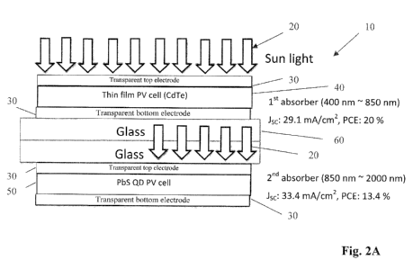
Figure 2A shows a cross-section of a solar panel according to an embodiment of
the
subject invention.
CA 02832129 2013-10-02
WO 2012/138651
PCT/US2012/031988
3
Figure 2B shows a cross-section of a solar panel according to another
embodiment of
the subject invention.
DETAILED DISCLOSURE
When the terms "on" or "over" are used herein, when referring to layers,
regions,
patterns, or structures, it is understood that the layer, region, pattern or
structure can be
directly on another layer or structure, or intervening layers, regions,
patterns, or structures
may also be present. When the terms "under" or "below" are used herein, when
referring to
layers, regions, patterns, or structures, it is understood that the layer,
region, pattern or
structure can be directly under the other layer or structure, or intervening
layers, regions,
patterns, or structures may also be present. When the term "directly on" is
used herein, when
referring to layers, regions, patterns, or structures, it is understood that
the layer, region,
pattern or structure is directly on another layer or structure, such that no
intervening layers,
regions, patterns, or structures are present.
When the term "about" is used herein, in conjunction with a numerical value,
it is
understood that the value can be in a range of 95% of the value to 105% of the
value, i.e. the
value can be +/- 5% of the stated value. For example, "about 1 kg" means from
0.95 kg to
1.05 kg.
When the term "sensitive" is used herein, in conjunction with describing a
photovoltaic cell being sensitive to a certain type of light or to photons
having a wavelength
of a given value or within a given range, it is understood that the
photovoltaic cell is capable
of absorbing the light to which it is sensitive and generating a carrier. When
the term "not
sensitive" or "insensitive" is used herein, in conjunction with describing a
photovoltaic cell
not being sensitive or being insensitive to a certain type of light or to
photons having a
wavelength of a given value or within a given range, it is understood that the
photovoltaic
cell is not able to absorb the light to which it is not sensitive and cannot
generate a carrier
from the absorption of the light.
It is to be understood that by "transparent," it is meant that at least a
portion of the
light to which an object is said to be transparent can pass through the object
without being
absorbed or reflected.
Embodiments of the subject invention relate to novel and advantageous solar
panels,
as well as methods of manufacturing the solar panels and method of using the
solar panels.
CA 02832129 2013-10-02
WO 2012/138651
PCT/US2012/031988
4
The solar panels and methods of use thereof can advantageously capture and
store solar
energy from a wider spectrum of photons than conventional photovoltaic cells.
In an embodiment, a solar panel can include: a first photovoltaic cell,
wherein the first
photovoltaic cell is sensitive to photons having a first one or more
wavelengths, wherein the
first one or more wavelengths are in a first wavelength range; and a second
photovoltaic cell,
wherein the second photovoltaic cell is sensitive to photons having a second
one or more
wavelengths, wherein the second one or more wavelengths are in a second
wavelength range,
such that at least one of the second one or more wavelengths is not in the
first wavelength
range, and at least one of the first one or more wavelengths is not in the
second wavelength
range. At least one of the second one or more wavelengths can be greater than
1 um. In a
further embodiment, the at least one of the second one or more wavelengths can
be at least
700 nm.
In another embodiment of the present invention, a method of fabricating a
solar panel
can include: foinfing a first photovoltaic cell, wherein the first
photovoltaic cell is sensitive to
photons having a first one or more wavelengths, wherein the first one or more
wavelengths
are in a first wavelength rang; forming a second photovoltaic cell, wherein
the second
photovoltaic cell is sensitive to photons having a second one or more
wavelengths, wherein
the second one or more wavelengths are in a second wavelength range, such that
at least one
of the second one or more wavelengths is not in the first wavelength range,
and at least one of
the first one or more wavelengths is not in the second wavelength range. At
least one of the
second one or more wavelengths can be greater than 1 pm. The method can
further comprise
coupling the first photovoltaic cell and the second photovoltaic cell. In a
further embodiment,
the at least one of the second one or more wavelengths can be at least 700 nm.
In a further embodiment, a method of capturing and storing solar energy can
include
positioning a solar panel such that sunlight is incident on the solar panel,
wherein the solar
panel includes: a first photovoltaic cell, wherein the first photovoltaic cell
is sensitive to
photons having a first one or more wavelengths, wherein the first one or more
wavelengths
are in a first wavelength rang; and a second photovoltaic cell, wherein the
second
photovoltaic cell is sensitive to photons having a second one or more
wavelengths, wherein
the second one or more wavelengths are in a second wavelength range, such that
at least one
of the second one or more wavelengths is not in the first wavelength range,
and at least one of
the first one or more wavelengths is not in the second wavelength range. At
least one of the
CA 02832129 2013-10-02
WO 2012/138651
PCT/US2012/031988
second one or more wavelengths can be greater than 1 um. In a further
embodiment, the at
least one of the second one or more wavelengths can be at least 700 nm.
Embodiments of the subject invention relate to a method and apparatus for
providing
a novel solar panel structure harvesting photons from the visible range up to
the infrared
5 range in the solar spectrum by integrating an IR photovoltaic cell on a
photovoltaic cell, such
as a conventional thin film photovoltaic cell. While the solar spectrum ranges
from 350 nm
to 2500 nm, conventional thin film photovoltaic cells have no infrared
sensitivity beyond 1
um. That is, related art photovoltaic cells are not sensitive to photons
having wavelengths
greater than 1 um and cannot capture and/or store energy from such photons. As
is known in
the art, the visible range of the spectrum is from 380 nm to 750 nm,
inclusive.
Referring to Figure 1A, a solar panel according to an embodiment of the
subject
invention can result in an increased power conversion efficiency (PCE). Figure
IA shows
spectral irradiance (W/m2nm) vs. wavelength (nm) of the incident light. For an
inorganic
photovoltaic cell (for example, including CdTe), which is sensitive to light
having a
wavelength in the range of from about 400 nm to about 850 nm, if all the
photons in the range
of from about 400 nm to about 850 nm are converted to the carriers, Jsc is
29.1 mA/cm2 and
if Voc is 0.85 V and the fill factor (FE) is 80%, PCE is 20%. For an IR
photovoltaic cell
including PbS quantum dots and sensitive to light having a wavelength in the
range of from
about 700 nm to about 2000 nm, if all the photons in the range of from about
700 nm to about
2000 nm are converted to the carriers, Jsc is 44.0 mA/cm2 and if Voc is 0.5 V
and FF is 80%õ
PCE is 17.6%. For an IR photovoltaic cell including PbS quantum dots and
sensitive to light
having a wavelength in the range of from about 850 nm to about 2000 nm, if all
the photons
in the range of from about 850 nm to about 2000 nm are converted to the
carriers, Jsc is 33.4
mA/cm2 and if Voc is 0.5 V and FF is 80%, PCE is 13.4%.
Infrared photodetectors using solution-processable nanocrystals (e.g., PbS or
PbSe
nanocrystals) have been described in United States Patent Application Serial
No. 13/272,995
(filed October 13, 2011), which claims priority to United States Provisional
Patent
Application Serial No. 61/416,630 (filed November 23, 2010), the disclosures
of both of
which are hereby incorporated by reference in their entirety. Such IR
photodetectors have
been shown to be compatible with large area manufacturing. In embodiments of
the subject
invention, an IR photovoltaic cell can have a structure similar to that of the
infrared
photodetector described in United States Patent Application Serial No.
13/272,995, which
claims priority to United States Provisional Patent Application Serial No.
61/416,630, and/or
CA 02832129 2013-10-02
WO 2012/138651
PCT/US2012/031988
6
similar to that of the infrared photodetector described in United States
Provisional Patent
Application Serial No. 61/416,630. Also, referring to Figure 1B, which shows
the
absorbance of PbSe quantum dots, PbSe quantum dots have infrared sensitivity.
When an IR photovoltaic cell is integrated on a photovoltaic cell (such as a
conventional thin film photovoltaic cell), a high efficiency photovoltaic
panel can be realized.
Embodiments of the subject invention relate to novel photovoltaic panels for
harvesting a
large portion of the solar spectrum by integrating an IR photovoltaic cell on
a photovoltaic
cell (such as a conventional thin film photovoltaic cell). In some
embodiments, a
photovoltaic panel can harvest the entire solar spectrum.
Referring to Figure 2A, in an embodiment of the subject invention, a solar
panel 10
can include a photovoltaic cell 40 and an IR photovoltaic cell 50. The
photovoltaic cell 40
can be, for example, a thin film photovoltaic cell and can include cadmium
telluride (CdTe),
copper indium gallium selenide (CIGS), amorphous silicon (a-Si), and/or
polysilicon (poly-
Si), though embodiments are not limited thereto. In many embodiments, the
photovoltaic cell
40 is not sensitive to photons having a wavelength greater than 1 pun. For
example, the
photovoltaic cell 40 can be sensitive to photons in the visible range. In one
embodiment, the
photovoltaic cell 40 can be sensitive to photons having a wavelength of from
about 400 nm to
about 850 nm.
The IR photovoltaic cell 50 is sensitive to photons having a wavelength
greater than 1
um. In an embodiment, the IR photovoltaic cell 50 is sensitive to photons
having a
wavelength up to 2500 nm. In another embodiment, the IR photovoltaic cell 50
is sensitive to
photons having a wavelength up to about 2000 nm. In a further embodiment, the
IR
photovoltaic cell 50 is sensitive to photons having a wavelength up to 2000
nm. In yet a
further embodiment, the IR photovoltaic cell 50 is sensitive to photons having
a wavelength
in a range of from about 850 nm to about 2000 nm.
It is to be understood that, in this description and in the appended claims,
when a
photovoltaic cell 40 or IR photovoltaic cell 50 is described as sensitive to
photons having a
wavelength of a given value, in a given range, or of at least a certain value,
this does not
preclude the photovoltaic cell 40 or IR photovoltaic cell 50 from being
sensitive to photons
having a wavelength different from the given value, outside the given range,
or of less than
the certain value, unless explicitly stated. That is, in this description and
in the appended
claims, when a photovoltaic cell 40 or IR photovoltaic cell 50 is described as
sensitive to
photons having a wavelength of a given value, in a given range, or of at least
a certain value,
CA 02832129 2013-10-02
WO 2012/138651
PCT/US2012/031988
7
the photovoltaic cell 40 or IR photovoltaic cell 50 is sensitive to at least
those photons and
may or may not also be sensitive to photons having a wavelength different from
the given
value, outside the given range, or of less than the certain value, unless it
is explicitly stated
that the photovoltaic cell 40 or IR photovoltaic cell 50 is only sensitive to
photons having the
stated value or in the stated range or that the photovoltaic cell 40 or IR
photovoltaic cell 50 is
not sensitive to photons having a given value, within a given range, or
greater than a certain
value.
In various embodiments, the IR photovoltaic cell 50 can be sensitive to
photons
having a wavelength of at least any of the following values (all values are in
pm): 0.20, 0.21,
0.22, 0.23, 0.24, 0.25, 0.26, 0.27, 0.28, 0.29, 0.30, 0.31, 0.32, 0.33, 0.34,
0.35, 0.36, 0.37,
0.38, 0.39, 0.40, 0.41, 0.42, 0.43, 0.44, 0.45, 0.46, 0.47, 0.48, 0.49, 0.50,
0.51, 0.52, 0.53,
0.54, 0.55, 0.56, 0.57, 0.58, 0.59, 0.60, 0.61, 0.62, 0.63, 0.64, 0.65, 0.66,
0.67, 0.68, 0.69,
0.70, 0.71, 0.72, 0.73, 0.74, 0.75, 0.76, 0.77, 0.78, 0.79, 0.80, 0.81, 0.82,
0.83, 0.84, 0.85,
0.86, 0.87, 0.88, 0.89, 0.90, 0.91, 0.92, 0.93, 0.94, 0.95, 0.96, 0.97, 098,
0.99, 1.00, 1.01,
1.02, 1.03, 1.04, 1.05, 1.06, 1.07, 1.08, 1.09, 1.10, 1.11, 1.12, 1.13, 1.14,
1.15, 1.16, 1.17,
1.18, 1.19, 1.20, 1.21, 1.22, 1.23, 1.24, 1.25, 1.26, 1.27, 1.28, 1.29, 1.30,
1.31, 1.32, 1.33,
1.34, 1.35, 1.36, 1.37, 1.38, 1.39, 1.40, 1.41, 1.42, 1.43, 1.44, 1.45, 1.46,
1.47, 1.48, 1.49,
1.50, 1.51, 1.52, 1.53, 1.54, 1.55, 1.56, 1.57, 1.58 ,1.59, 1.60, 1.61, 1.62,
1.63, 1.64, 1.65,
1.66, 1.67, 1.68, 1.69, 1.70, 1.71, 1.72, 1.73, 1.74, 1.75, 1.76, 1.77, 1.78,
1.79, 1.80, 1.81,
1.82, 1.83, 1.84, 1.85, 1.86, 1.87, 1.88, 1.89, 1.90, 1.91, 1.92, 1.93, 1.94,
1.95, 1.96, 1.97,
1.98, or 1.99 (i.e., the IR photovoltaic cell 50 can he sensitive to photons
having a wavelength
of: at least 0.20 m, at least 0.21 pm, ..., at least 1.99 p.m). In further
embodiments, the IR
photovoltaic cell 50 can be sensitive to only those photons having a
wavelength of at least
any of the following values (all values are in pm), while not being sensitive
to any photons
having a wavelength of less than the value: 0.20, 0.21, 0.22, 0.23, 0.24,
0.25, 0.26, 0.27, 0.28,
0.29, 0.30, 0.31, 0.32, 0.33, 0.34, 0.35, 0.36, 0.37, 0.38, 0.39, 0.40, 0.41,
0.42, 0.43, 0.44,
0.45, 0.46, 0.47, 0.48, 0.49, 0.50, 0.51, 0.52, 0.53, 0.54, 0.55, 0.56, 0.57,
0.58, 0.59, 0.60,
0.61, 0.62, 0.63, 0.64, 0.65, 0.66, 0.67, 0.68, 0.69, 0.70, 0.71, 0.72, 0.73,
0.74, 0.75, 0.76,
0.77, 0.78, 0.79, 0.80, 0.81, 0.82, 0.83, 0.84, 0.85, 0.86, 0.87, 0.88, 0.89,
0.90, 0.91, 0.92,
0.93, 0.94, 0.95, 0.96, 0.97, 098, 0.99, 1.00, 1.01, 1.02, 1.03, 1.04, 1.05,
1.06, 1.07, 1.08,
1.09, 1.10, 1.11, 1.12, 1.13, 1.14, 1.15, 1.16, 1.17, 1.18, 1.19, 1.20, 1.21,
1.22, 1.23, 1.24,
1.25, 1.26, 1.27, 1.28, 1.29, 1.30, 1.31, 1.32, 1.33, 1.34, 1.35, 1.36, 1.37,
1.38, 1.39, 1.40,
1.41, 1.42, 1.43, 1.44, 1.45, 1.46, 1.47, 1.48, 1.49, 1.50, 1.51, 1.52, 1.53,
1.54, 1.55, 1.56,
CA 02832129 2013-10-02
WO 2012/138651
PCT/US2012/031988
8
1.57, 1.58 ,1.59, 1.60, 1.61, 1.62, 1.63, 1.64, 1.65, 1.66, 1.67, 1.68, 1.69,
1.70, 1.71, 1.72.
1.73, 1.74, 1.75, 1.76, 1.77, 1.78, 1.79, 1.80, 1.81, 1.82, 1.83, 1.84, 1.85,
1.86, 1.87, 1.88,
1.89, 1.90, 1.91, 1.92, 1.93, 1.94, 1.95, 1.96, 1.97, 1.98, or 1.99 (i.e. the
IR photovoltaic cell
50 can be sensitive to only those photons having a wavelength of: at least
0.20 JIM, at least
0.21 m, ..., at least 1.99 pm; while not being sensitive to any photons
having a wavelength
of less than 0.20 pm, 0.21 pm, ..., 1.99 um, respectively). In a preferred
embodiment, the IR
photovoltaic cell 50 is sensitive to photons having a wavelength of greater
than l micron. In
another preferred embodiment, the IR photovoltaic cell 50 is sensitive to
photons having a
wavelength of at least 0.70 microns. In yet another preferred embodiment, the
IR
photovoltaic cell 50 is sensitive to photons having a wavelength of at least
0.85 microns.
In certain embodiments, the IR photovoltaic cell 50 can include an IR
sensitizing
layer including quantum dots. The quantum dots can be, for example, PbS or
PbSe quantum
dots, though embodiments are not limited thereto.
In many embodiments, the solar panel 10 can include a electrode 30 on one or
both
sides of the photovoltaic cell 40 and/or the IR photovoltaic cell 50. In one
embodiment, both
the photovoltaic cell 40 and the IR photovoltaic cell 50 include a transparent
anode and a
transparent cathode. Each electrode layer 30 can be any transparent electrode
known in the
art, for example, a layer including indium tin oxide (ITO), carbon nanotubes
(CNTs), indium
zinc oxide (IZO), a silver nanowire, and/or a magnesium:silver/A1q3
(iVig:Ag/Alq3) stack
layer. Each electrode layer 30 can include a transparent conductive oxide
(TCO), including a
TCO other than those explicitly listed herein. In a specific embodiment, one
or more of the
transparent electrode layers can be a Mg:Ag/A1q3 stack layer such that the
Mg:Ag layer has a
ratio of 10:1 (Mg:Ag). The Mg:Ag layer can have a thickness of less than 30
nm, and the
A1q3 layer can have a thickness of from 0 nm to 200 nm. Each electrode layer
30 can be
transparent to at least a portion of the light in the visible region of the
spectrum. Each
electrode layer 30 can be transparent to at least a portion, and preferably
all, of the light in the
infrared region of the spectrum. In certain embodiments, each electrode layer
30 can be
transparent to at least a portion, and preferably all, of the light in the
visible region of the
spectrum and at least a portion, and preferably all, of the light in the
infrared region of the
spectrum. In an embodiment, the solar panel 10 can include a glass substrate
60 between the
photovoltaic cell 40 and the IR photovoltaic cell 50. For example, the IR
photovoltaic cell 50
can be fabricated on the glass substrate 60, and then the glass substrate 60
can be coupled
onto the photovoltaic cell 40 which may also include a glass substrate 60.
CA 02832129 2013-10-02
WO 2012/138651
PCT/US2012/031988
9
Referring to Figure 2B, in another embodiment, the solar panel 10 can use a
structure
that positions argon gas in between the photovoltaic cell 40 and the IR
photovoltaic cell 50
such that the light exiting the photovoltaic cell 40 passes through the argon
gas before
entering the IR photovoltaic cell 50. A specific embodiment utilizes a chamber
70 housing
argon gas. The photovoltaic cell 40 and the IR photovoltaic cell 50 can both
be partially, or
entirely, positioned within the chamber 70 and/or can form a part of the
chamber 70. For
example, the photovoltaic cell 40 and the IR photovoltaic cell 50 can each
optionally include
a glass substrate 60, and the glass substrate 60 of the photovoltaic cell 40
can serve as a top or
bottom of the chamber 70 with the glass substrate 60 of the IR photovoltaic
cell 50 also
serving as a top or bottom of the chamber 70.The solar panels 10 in accordance
with specific
embodiments of the subject invention can be configured such that incident
sunlight 20 is
incident upon both the photovoltaic cell 40 and the IR photovoltaic cell 50
and at least a
portion of the sunlight 20 is absorbed by the photovoltaic cell 40 and at
least a portion of the
sunlight 20 is absorbed by the IR photovoltaic cell 50. Such configurations
are shown in
Figures 2A and 2B in which the sunlight 20 is incident upon the photovoltaic
cell 40 and is
incident upon the a photovoltaic cell 50 after passing through the (optional)
glass
substrate(s) 60 (in Figure 2A) or the argon gas (in Figure 2B).
Though the electrode layers 30 are labeled in Figures 2A and 2B as
transparent,
embodiments are not limited thereto. That is, each electrode layer 30 can be
transparent to at
least a portion of visible light and/or at least a portion of IR light but may
not be transparent
to at least a portion of visible light and/or at least a portion of IR light.
In an embodiment, the top electrode 30 of the photovoltaic cell 40 can be an
anode or
a cathode and is transparent to at least a portion of visible light and at
least a portion of IR
light. The bottom electrode 30 of the photovoltaic cell 40 can be an anode or
a cathode and is
transparent to at least a portion of IR light and may be transparent to at
least a portion of
visible light. The top electrode 30 of the IR photovoltaic cell 50 can be an
anode or a cathode
and is transparent to at least a portion of IR light and may be transparent to
at least a portion
of visible light. The bottom electrode 30 of the IR photovoltaic cell 50 can
be an anode or a
cathode and may be transparent to at least a portion of IR light and may be
transparent to at
least a portion of visible light.
In certain embodiments, the solar panel 10 can be operated in "upside down"
mode
such that light is incident on the bottom electrode 30 of the IR photovoltaic
cell 50. In a
particular embodiment, the bottom electrode 30 of the IR photovoltaic cell 50
can be an
CA 02832129 2013-10-02
WO 2012/138651
PCT/US2012/031988
anode or a cathode and is transparent to at least a portion of visible light
and at least a portion
of IR light. The top electrode 30 of the IR photovoltaic cell 50 can be an
anode or a cathode
and is transparent to at least a portion of visible and may be transparent to
at least a portion of
IR light. The bottom electrode 30 of the photovoltaic cell 40 can be an anode
or a cathode
5 and is transparent to at least a portion of visible light and may be
transparent to at least a
portion of IR light. The top electrode 30 of the photovoltaic cell 40 can be
an anode or a
cathode and may be transparent to at least a portion of IR light and may be
transparent to at
least a portion of visible light.
In many embodiments, the solar panel 10 can be configured such that light
incident on
10 an input surface of the photovoltaic cell 40, which passes through the
photovoltaic cell 40 and
exits an output surface of the first photovoltaic cell 40, is incident on an
input surface of the
IR photovoltaic cell 50 and enters the IR photovoltaic cell 50. In another
embodiment, the
solar panel 10 can be configured such that light incident on an input surface
of the IR
photovoltaic cell 50, which passes through the IR photovoltaic cell 50 and
exits an output
surface of the IR photovoltaic cell 50, is incident on an input surface of the
photovoltaic cell
40 and enters the photovoltaic cell 40.
In one embodiment of the subject invention, a method of capturing and storing
solar
energy can include positioning a solar panel such that sunlight is incident on
the solar panel,
wherein the solar panel includes: a photovoltaic cell, wherein the
photovoltaic cell is sensitive
to photons having a wavelength in the visible range; and an infrared
photovoltaic cell,
wherein the infrared photovoltaic cell is sensitive to photons having a
wavelength greater
than 1 um. The solar panel can be as described herein with reference to
Figures 2A and 2B.
In many embodiments, the photovoltaic cell is not sensitive to photons having
a wavelength
greater than 1 um. For example, the photovoltaic cell can be sensitive to
photons in the
visible range. In one embodiment, the photovoltaic cell can be sensitive to
photons having a
wavelength of from about 400 nm to about 850 nm.
In many embodiments, light incident on an input surface of the photovoltaic
cell 40
can pass through the photovoltaic cell 40 and exit an output surface of the
first photovoltaic
cell 40, and can then be incident on an input surface of the IR photovoltaic
cell 50 and enter
the IR photovoltaic cell 50. In another embodiment, light incident on an input
surface of the
IR photovoltaic cell 50 can pass through the IR photovoltaic cell 50 and exit
an output
surface of the IR photovoltaic cell 50, and can then be incident on an input
surface of the
photovoltaic cell 40 and enter the photovoltaic cell 40.
CA 02832129 2013-10-02
WO 2012/138651
PCT/US2012/031988
11
The IR photovoltaic cell of the solar panel can be sensitive to at least
photons having
a wavelength greater than, for example, 1 um. In an embodiment, the 1R
photovoltaic cell is
sensitive to photons having a wavelength up to 2500 nm. In another embodiment,
the IR
photovoltaic cell is sensitive to photons having a wavelength up to about 2000
nm. In a
further embodiment, the IR photovoltaic cell is sensitive to photons having a
wavelength up
to 2000 nm. In yet a further embodiment, the IR photovoltaic cell is sensitive
to photons
having a wavelength in a range of from about 850 nm to about 2000 nm.
In certain embodiments, the IR photovoltaic cell can include an IR sensitizing
layer
including quantum dots. The quantum dots can be, for example, PbS or PbSe
quantum dots,
though embodiments are not limited thereto.
The solar panels of the subject invention can be configured such that incident
sunlight
is incident upon both the photovoltaic cell and the IR photovoltaic cell and
at least a portion
of the sunlight is absorbed by the photovoltaic cell and at least a portion of
the sunlight is
absorbed by the IR photovoltaic cell.
The subject invention also relates to methods of forming a solar panel. In an
embodiment, a method of fabricating a solar panel can include: forming a
photovoltaic cell,
wherein the photovoltaic cell is sensitive to photons having a wavelength in
the visible range;
forming an infrared photovoltaic cell, wherein the infrared photovoltaic cell
is sensitive to
photons having a wavelength greater than 1 um; and coupling the photovoltaic
cell and the
infrared photovoltaic cell.
The photovoltaic cell and the IR photovoltaic cell can be as described herein
with
reference to Figures 2A and 2B. In many embodiments, the photovoltaic cell is
not sensitive
to photons having a wavelength greater than 1 1.tm. For example, the
photovoltaic cell can be
sensitive to photons in the visible range but not to those having a wavelength
greater than 1
um. In one embodiment, the photovoltaic cell can be sensitive to photons
having a
wavelength of from about 400 nm to about 850 nm but not sensitive to photons
having a
wavelength less than about 400 nm or greater than about 850 nm.
The IR photovoltaic cell of the solar panel can be sensitive to at least
photons having
a wavelength greater than, for example, 1 um. In an embodiment, the IR
photovoltaic cell is
sensitive to photons having a wavelength up to 2500 nm. In another embodiment,
the IR
photovoltaic cell is sensitive to photons having a wavelength up to about 2000
nm. In a
further embodiment, the IR photovoltaic cell is sensitive to photons having a
wavelength up
CA 02832129 2013-10-02
WO 2012/138651
PCT/US2012/031988
12
to 2000 nm. In yet a further embodiment, the IR photovoltaic cell is sensitive
to photons
having a wavelength in a range of from about 850 nm to about 2000 nm.
In certain embodiments, the IR photovoltaic cell can include an IR sensitizing
layer
including quantum dots. The quantum dots can be, for example, PbS or PbSc
quantum dots,
though embodiments are not limited thereto.
The methods of fon-ning a solar panel according to the subject invention can
be
perfoinied such that the solar panel is configured such that incident sunlight
is incident upon
both the photovoltaic cell and the IR photovoltaic cell (i.e. at least a
portion of the sunlight is
absorbed by the photovoltaic cell and at least a portion of the sunlight is
absorbed by the IR
photovoltaic cell).
In many embodiments, a method of foi
__________________________________________ wing a solar panel can be performed
such that
light incident on an input surface of the photovoltaic cell 40 can pass
through the
photovoltaic cell 40 and exit an output surface of the first photovoltaic cell
40, and can then
be incident on an input surface of the IR photovoltaic cell 50 and enter the
IR photovoltaic
cell 50. In another embodiment, a method of foiming a solar panel can be
performed such
that light incident on an input surface of the IR photovoltaic cell 50 can
pass through the IR
photovoltaic cell 50 and exit an output surface of the IR photovoltaic cell
50, and can then be
incident on an input surface of the photovoltaic cell 40 and enter the
photovoltaic cell 40.
In an embodiment, the method of forming a solar panel can include fabricating
the IR
photovoltaic cell on a glass substrate and then coupling the glass substrate
to the photovoltaic
cell. The method can also include forming the photovoltaic cell on a glass
substrate such that
the glass substrate of the IR photovoltaic cell is coupled to the glass
substrate of the
photovoltaic cell.
In a further embodiment, the IR photovoltaic cell can be coated on an
optically clear
plastic film, and then the optically clear plastic film can be laminated on
the photovoltaic cell.
In yet a further embodiment, the method of foiming a solar panel can include
forming
a solar panel using a structure that positions gas, such as argon gas in
between a photovoltaic
cell and an IR photovoltaic cell such that the light exiting the photovoltaic
cell passes through
the gas before entering the IR photovoltaic cell. The gas can be, for example,
argon gas,
though embodiments are not limited thereto. A specific embodiment can include
forming a
chamber housing gas (e.g., argon gas). The photovoltaic cell 40 and the IR
photovoltaic cell
50 can both be partially, or entirely, positioned within the chamber 70 and/or
can form a part
of the chamber 70. In certain embodiments, the IR photovoltaic cell can be
fabricated on a
CA 02832129 2013-10-02
WO 2012/138651
PCT/US2012/031988
13
glass substrate, the photovoltaic cell can be fabricated on a separate glass
substrate, the walls
of the chamber can be formed, and then the IR photovoltaic cell and the
photovoltaic cell can
be brought into contact with the chamber walls such that the glass substrates
form the top and
bottom of the chamber, as depicted in Figure 2B.
The fabrication of IR photodetectors was described in previously-referenced
United
States Patent Application Serial No. 13/272,995 (filed October 13, 2011),
which claims
priority to United States Provisional Patent Application Serial No. 61/416,630
(filed
November 23, 2010), and/or was described in United States Provisional Patent
Application
Serial No. 61/416,630 (filed November 23, 2010), and will now be described
again in detail.
United States Patent Application Serial No. 13/272,995 (filed October 13,
2011),
which claims priority to United States Provisional Patent Application Serial
No. 61/416,630
(filed November 23, 2010), and/or United States Provisional Patent Application
Serial No.
61/416,630 (filed November 23, 2010) describe an infrared photodetector with
high
detectivity for use as a sensor and for use in up-conversion devices. When the
dark current is
the dominant noise factor, detectivity can be expressed as the following
equation (1).
D* = RI (2qJd)1/2 (1)
where R is the responsivity, id is the dark current density, and g is the
elementary charge (1.6
x 10-19 C). To achieve a photodetector with an optimal detectivity, a very low
dark current
density is required. The photodeteetors according to embodiments of the
invention include a
hole blocking layer (HBL) with a deep highest occupied molecule orbital (HOMO)
and an
electron blocking layer (EBL) with a high lowest unoccupied molecule orbital
(LUMO)
where the EBL is situated on the anode facing surface and the HBL is situated
on the cathode
facing surface of an IR photosensitive layer. The layers can range from about
20 nm to about
500 nm in thickness, and where the overall spacing between electrodes is less
than 5 pm. The
IR photodetector according to embodiments of the invention allows high
detectivity at
applied voltages less than 5V.
The TR photosensitive layer can he an organic or organometallic including
material or
an inorganic material. The material can absorb through a large portion of the
IR extending
beyond the near IR (700 to 1400 nm), for example to wavelengths up to 1800 nm,
2000, nm,
2500 nm or greater. Exemplary organic or organometallic including materials
include:
perylene-3,4,9,10-tetracarboxylic-3,4,9,10-dianhydride (PCTDA), tin (II)
phthalocyanine
CA 02832129 2013-10-02
WO 2012/138651
PCT/US2012/031988
14
(SnPc), SnPc:C60, aluminum phthalocyanine chloride (A1PcC1), A1PcC1:C60,
titanyl
phthalocyanine (Ti0Pc), and Ti0Pc:C60. Inorganic materials for use as
photosensitive layers
include: PbSe quantum dots (QDs), PbS QDs, PbSe thin films, PbS thin films,
InAs, InGaAs,
Si, Ge, and GaAs.
The HBL can be an organic or organometallic including material including, but
not
limited to: 2,9-Dim eth y1-4, 7-dipheny1-1 ,1 0-phenanthroline
(BCP), p-
bis(triphenyl silyl)benzene (UGH2), 4, 7-diphenyl- 1 , 1 0-phenanthroline
(BPhen), tri s- (8 -
hydroxy quinoline) aluminum (A1q3), 3,5'-NN'-dicarbazole-benzene (mCP), C60,
and tris[3-
(3-pyridy1)-mesityl]borane (3TPYMB). Alternatively, the HBL can be an
inorganic material
including, but not limited to thin films or nanoparticles of ZnO or Ti02.
The EBL can be an organic material, for example, but not limited to poly(9,9-
dioctyl-
fluorenc-co-N-(4-butylphenyl)diphenylamine) (TFB),
1,1 -bis [(di-4-
tolylamino)phenyl]cyclohexane (TAPC), /V,N'-diphenyl-N,AP(2-naphthyl)-(1,1'-
pheny1)-4,4'-
diamine (NPB), N,N'-diphenyl-N,N'-di(m-toly1) benzidine (TPD), poly-N,N'-bis-4-
butylphenyl-N,N'-bis-phenylbenzidine (poly-TPD), or polystyrene-N,N-diphenyl-
N,N-bis(4-
n-butylpheny1)-(1, 1 0-biphenyl)-4,4-diamine-perfluorocyclobutane (PS-TPD-
PFCB).
Photodetectors were prepared having no blocking layer, poly-TPD as an EBL, ZnO
nanoparticles as a HBL, and with poly-TPD and ZnO nanoparticles as an EBL and
a HBL,
respectively, where the IR photosensitive layer included PbSe nanocrystals.
The dark
current-voltage (J-V) plots for the photodetectors decreased by more than 3
orders of
magnitude for that with an EBL and a HBL from the photodetector that is
blocking layer free.
The photodetector with both blocking layers shows a detectivity of more than
1011 Jones over
IR and visible wavelengths smaller than 950 nm.
Inorganic nanoparticle photodetectors were also constructed having no blocking
layers and with EBL and HBL layers. The photodetector included various HBLs
(BCP, C60,
or ZnO), EBLs (TFB or poly-TPD), and PbSe quantum dots included the IR
photosensitive
layer. Although the magnitude of reduction differs, placement of an EBL and a
HBL are
placed on the PbSe including photodetector results in a significant reduction
of the dark
current at low applied voltages.
All patents, patent applications, provisional applications, and publications
referred to
or cited herein are incorporated by reference in their entirety, including all
figures and tables,
to the extent they are not inconsistent with the explicit teachings of this
specification.
CA 02832129 2013-10-02
WO 2012/138651
PCT/US2012/031988
It should be understood that the examples and embodiments described herein are
for
illustrative purposes only and that various modifications or changes in light
thereof will be
suggested to persons skilled in the art and are to be included within the
spirit and purview of
this application.
5