Note: Descriptions are shown in the official language in which they were submitted.
I 4
CA 02832477 201.3-10-07
OPTICAL SECURITY COMPONENT HAVING A TRANSMISSIVE EFFECT,
MANUFACTURE OF SUCH A COMPONENT, AND SECURE DOCUMENT
PROVIDED WITH SUCH A COMPONENT
FIELD OF THE INVENTION
The present invention relates to the field of security markings. More
particularly, it relates to a transmissive optical security component for
verifying the
authenticity of a document, to a method for manufacturing such a component and
to a secure
document equipped with such a component.
PRIOR ART
Many technologies for authenticating documents or products, and especially for
securing documents, such as documents of value, i.e. banknotes, passports, or
identification
documents, etc., are known. These technologies aim to produce optical security
components
the optical effects of which take very characteristic and verifiable
configurations depending
on the parameters of the observation (orientation relative to the axis of
observation, position
and dimensions of the light source, etc.). The general aim of these optical
components is to
produce novel and differentiated effects from physical configurations that are
difficult to
reproduce.
Among these components, DON/IDs (for diffractive optically variable image
devices) are optical components, commonly called holograms, which produce
variable
diffractive images. These components are generally observed in reflection.
The present patent application relates to optical security components that can
be
checked in transmission.
Among these components, patent US 6 428 051 describes a document of value,
of the banknote type, comprising an aperture forming a window covered by a
security film,
the security film being fixed by an adhesive to the perimeter of the window
formed in the
document, and comprising a certain number of authenticating features.
In the article by I. Aubrecht et al. ("Polarization-sensitive multilayer
diffractive
structures for document security", Proceedings of SPIE Vol. 7358, 2009) a
multilayer
CA 02832477 2013-10-07
=
2
structure is described exhibiting resonant transmission effects based on the
excitation of
plasmonic modes at the interfaces between a structured metal layer and two
dielectric layers
encapsulating the metal layer. This article reports the polarization
dependence of the effect
and proposes a system for checking the authenticity of a component produced in
this way
based on analysis of the polarization of the transmitted wave.
Patent application US 2010/0307705 describes, in a general way, a security
document with a region comprising nanoscale metal patterns for exciting bulk
or surface
plasmons and generating resonant effects.
The structures described in the aforementioned documents, although they
exhibit remarkable effects in transmission or reflection, are not however easy
to authenticate
with the naked eye, especially as regards authentication in transmission by an
inexperienced
user.
The present invention provides a plasmonic optical security component that can
be very easily and very securely checked in transmission with the naked eye,
in order to
provide an uninitiated user with a maximum of comfort while guaranteeing
authentication
with a very high reliability.
SUMMARY OF THE INVENTION
According to a first aspect, the invention relates to a plasmonic optical
security
component intended to be observed in transmission, said optical component
comprising two
transparent dielectric layers, and a metal layer arranged between said
dielectric layers in
order to form two dielectric/metal interfaces, at least one part of the area
of the metal layer
being structured to form corrugations that are able to couple surface plasmon
modes
supported by said dielectric/metal interfaces with an incident light wave. The
corrugations
are arranged in a first main direction in a first coupling zone, and in a
second main direction,
substantially perpendicular to the first main direction, in at least one
second coupling zone
separate from the first coupling zone, said metal layer being continuous in
each of said
coupling zones.
Such a component exhibits an extraordinary transmission effect in a spectral
band centered on what is called a central wavelength, defined by the
characteristics of the
corrugations of the coupling zones, and for an observer, variations in color
of the coupling
CA 02832477 2013-10-07'
3
zones with the angle of observation of the component, enabling easy and
reliable
authentication of the security component.
More precisely, at least two of said coupling zones contain corrugations
arranged in two substantially perpendicular main directions, the component
exhibiting, when
observed in transmission, a marked visual contrast between a first zone, the
color of which is
stable with the angle of observation of the component, and a second highly
variable zone.
As a variant, these coupling zones form complementary patterns, making
authentication by an observer even easier, the patterns allowing the movements
that will
allow a large variation in color to be generated to be made more intuitive for
the observer.
As another variant, at least one part of the corrugations are arranged
concentrically or radially, in such a way as to make the component axially
symmetric. The
observation is then independent of azimuth.
As another variant, the metal layer furthermore comprises an unstructured
zone.
This zone of high optical density makes it possible to further accentuate the
coupling zones,
which exhibit, in a given spectral band, an extraordinary transmission due to
the plasmonic
effect.
Advantageously, the corrugations in the coupling zones have a pitch between
100 nm and 600 nm and a depth between 10% and 30% of the pitch. The pitch of
the various
coupling zones may be identical in order to exhibit similar colors when
observed by an
observer, or in contrast different colors depending on the desired visual
effect.
Advantageously, the difference between the refractive indices of said
transparent dielectrics, in the targeted spectral band, preferably the
visible, forming each of
said layers is less than 0.1, enabling an optimal extraordinary transmission
effect at said
central wavelength.
As a variant, at least one part of the metal layer is formed of silver and its
thickness is substantially comprised between 20 and 60 nm.
As another variant, at least one part of the metal layer is formed of aluminum
and its thickness is substantially comprised between 10 and 30 nm.
In one embodiment, the metal layer may be formed of a single metal. The layer
then has a substantially constant thickness.
According to another embodiment, the metal layer comprises at least two parts
CA 02832477 201.3-10-07
4
each of which is formed of a different metal. This may enable different visual
effects to be
obtained, both in reflection and in transmission, in the spectral band of the
plasmonic effect.
According to a second aspect, the invention relates to an optical security
element intended to secure a document and comprising at least one optical
security
component according to the first aspect. The security element may comprise
other security
components, for example holographic components.
As a variant, the security element comprises, depending on the circumstances,
other layers required for the final application; for example, the security
element may
comprise, in addition to the active layers generating the plasmonic effect, a
supporting film
bearing one of said dielectric layers and/or an adhesive film placed on one of
said
transparent dielectric layers. These films are neutral with respect to the
plasmonic effect
because they neither degrade nor affect the dielectric/metal interface. They
make it easier to
bond the element to a document to be secured and/or to apply it industrially.
According to a third aspect, the invention relates to a secure document
comprising a support and an optical security element according to the second
aspect, the
optical security element being fixed to said support, said support comprising
a transparent
zone on which said plasmonic optical security component is arranged.
The secure document, for example a document of value, such as a banknote, or
an authentication document, such as an identity card, may, by virtue of the
plasmonic optical
security component according to the invention, be easily checked in
transmission, and has a
high resistance to counterfeiting due to the technology employed.
As a variant, the optical security component according to the first aspect or
the
optical security element according to the second aspect is encapsulated in the
support of the
secure document. Transparent zones are provided on either side of the optical
security
component, thus enabling it to be checked in transmission.
According to a fourth aspect, the invention relates to a method for
manufacturing a plasmonic optical security component, comprising:
- depositing a metal layer on a first transparent dielectric layer; and
- encapsulating said metal layer with a second dielectric layer, in order to
form
two dielectric/metal interfaces, at least one part of the area of the metal
layer being
structured to form corrugations that are able to couple surface plasmon modes
supported by
CA 02832477 2013-10-07
said dielectric/metal interfaces with an incident light wave, the corrugations
being arranged
in a first main direction in a first coupling zone, and in a second main
direction, substantially
perpendicular to said first main direction, in at least one second coupling
zone separate from
the first coupling zone, said metal layer being continuous in each of said
coupling zones.
5 As a
variant, said first dielectric layer is structured to form said corrugations,
and the metal layer is deposited, with a substantially constant thickness, on
said thus
structured first layer.
As another variant, the deposition of the metal layer comprises depositing a
first
layer comprising a first metal on a first part of the surface of said first
dielectric layer and
depositing at least one second layer comprising a second metal on a second
part of the
surface of said first dielectric layer.
As a variant, the deposition of the metal layer is carried out selectively,
allowing
macroscopic patterns that are visible to the naked eye in transparency to be
defined. These
patterns correspond to demetallized zones, which will thus be transparent in
the visible,
these zones possibly being used to increase the resistance of the component to
counterfeiting
and optionally to increase how easily the person in charge of checking can
read the graphic
by framing, for example, one of the colored zones.
BRIEF DESCRIPTION OF THE FIGURES
Other features and advantages of the invention will become apparent on reading
the following description, which is illustrated by the figures in which:
figures IA and 1B, partial views, respectively of a cross section and from
above,
of an optical security component according to the invention;
figures 2A and 2B, numerical simulations showing the variation in the
intensity
of the transmitted wave as a function of wavelength and angle of incidence for
a component
of the type shown in figure 1A, in TM mode and TE mode with an azimuth of 00
and 900
,
respectively;
figures 3A to 3D, figures illustrating the effect obtained by observation of
the
component in transmission, in various configurations;
figure 4, an embodiment of a component having two structured zones with two
orthogonal grating vectors;
CA 02832477 2013-10-07
6
figures 5A and 5B, numerical simulations showing the variation in the
intensity
of the transmitted wave as a function of wavelength and tilt in the two zones
of the
component shown in figure 4;
figures 6A and 6B, transmission curves for a component of the type illustrated
in figure 4 as a function of wavelength for two angles of incidence;
figures 7A to 7D, schematics illustrating, in various configurations, an
example
security component according to the invention;
figures 8A to 8C, two other example security components according to the
invention;
figures 9A and 9B, another example security component according to the
invention;
figure 10, a figure illustrating a cross-sectional view of a variant of a
security
component according to the invention;
figures 11A to 11C, views, from above, below and in cross section,
respectively,
of an example secure document comprising a security component according to the
invention;
and
figures 12A and 12B, cross-sectional views of two variants of an example
secure document comprising an optical security component according to the
invention.
DETAILED DESCRIPTION
Figures 1A and 1B show partial views, a cross-sectional view and a top view
respectively, of one embodiment of a security component 10 according to the
invention.
The security component according to the invention generally comprises a
continuous metal layer 102 of substantially constant (typically between a few
tens to 80
nanometers) thickness t, which metal layer 102 is arranged between two
transparent
dielectric layers 101, 103 in order to form two dielectric/metal interfaces
105, 106. The
metal may be any metal capable of supporting plasmonic resonance, and is
preferably silver,
aluminum, gold, chromium, or copper. The dielectrics may be any dielectric
material that
can be "non-destructively associated" with the metal, i.e. any dielectric for
which there is no
risk of a physico-chemical reaction, for example oxidation, occurring that
would degrade the
effect to be checked. The dielectrics used for the layers 101, 103 have
substantially identical,
CA 02832477 2013-10-07
7
typically about 1.5, refractive indices, the difference between these indices
advantageously
being less than 0.1. For example, the dielectric layer 101 of refractive index
ni is a polymer
layer intended to be embossed, and the layer 103 is a dielectric polymer
encapsulating layer
of refractive index n2 substantially equal to n. The layers 101, 103 are
transparent in the
visible. It is known that, at the interface between a conductive material, for
example a metal,
and a dielectric, it is possible for a surface electromagnetic wave,
associated with a
collective oscillation of electrons at the surface, to propagate, this surface
electromagnetic
wave being called a surface plasmon. This phenomenon is, for example,
described in the
reference text by H. Raether (" Surface Plasmons", Springer-Verlag, Berlin
Heidelberg). An
incident light wave may be coupled to a plasmon mode in various ways,
especially by
structuring the interface to form a coupling grating.
This basic principle is implemented in the security component according to the
invention in order to obtain remarkable effects in transmission.
In the security component 10, the metal layer 102 is structured to form at
least
two separate coupling zones for coupling to an incident light wave. Each
coupling zone
comprises a set of substantially rectilinear and parallel corrugations, the
corrugations of the
various zones extending in non-parallel directions. In each coupling zone, the
metal layer is
continuous and deformed in such a way as to form said corrugations. Figures IA
and 1B
schematically show a set of corrugations 104 in one of the coupling zones.
Each set of
corrugations is characterized by its pitch A, the amplitude h of the
corrugations (height
between peak and trough) and the thickness t of the metal layer in the
coupling zone.
Typically, the pitch of the grating is comprised between 100 nm and 600 nm and
advantageously between 200 nm and 500 nm, the height being comprised between
10% and
45% of the pitch of the grating and advantageously between 10% and 30%. The
term
"corrugation" is understood to mean a continually varying deformation of the
metal layer,
which layer is continuous over the entire coupling zone. The profile of the
corrugations is
advantageously sinusoidal or quasi-sinusoidal; the Applicant has demonstrated
that a
deformation with a sinusoidal profile is acceptable provided its duty cycle is
kept between
40% and 60%. The thickness t of the metal layer must be sufficiently small to
allow
excitation of and coupling to surface plasmon modes at the two
metal/dielectric interfaces,
thus enabling a resonant transmission effect as will be described in more
detail below.
CA 02832477 2013-10-07'
8
An incident wave of TM polarization (transverse magnetic wave i.e. for which
the magnetic field H is perpendicular to the plane of incidence xz, which is
the plane of the
figure in figure 1A) is considered, this wave being incident on the grating
with an azimuth of
00 to the grating vector kg, and on the layer 103 with an angle of incidence 0
to the y-axis
normal to the plane of the grating formed by the corrugations 104. The grating
vector kg,
shown in figure 1B, is a vector in a direction perpendicular to the lines of
the grating and of
norm defined by kg = 27r/A , where A is the pitch of the grating.
In order for there to be coupling, i.e. for energy to be transferred between a
wave
incident on a dielectric medium of relative permittivity Ed, and a plasmon
mode, the
following equality must be satisfied (see H. Raether, ibid):
ksp = niko sin kg (1),
where:
ko is the wave number defined by lc, = 24/1. ; and
ksp is defined by Ifs, = nspko, where nsp is the effective index of the
plasmon,
given by:
n= Vaned /(in + ed) (2),
rp
in the case of a metal layer of infinite thickness, where Em and Ed are the
permittivities of the metal and of the dielectric, respectively.
It is thus possible to define a central wavelength X0, in which wavelength
coupling will occur at normal incidence (0 = 0 ). The central wavelength is
defined by:
A.0 = A / ncp (3).
Thus, the pitch of the grating will be chosen depending on the desired central
wavelength.
With the pitch of the grating fixed, the variation in the coupling wavelength
A, is
expressed at nonzero angle of incidence, and zero azimuth to the grating
network, by
equation (1), which can be split into two equations:
A =(nsp ¨n, sin 0)x A (4)
A =(nv, + ni sin 0)x A (5)
There are then two wavelengths at which it will be possible for the incident
CA 02832477 2016-08-04
54373-13PPH
9
wave to couple to a surface plasmon, corresponding to co-propagating and
contra-propagating
plasmon modes, respectively.
When the metal layer is of finite thickness and, in addition, its thickness is
of the
same order of magnitude as the penetration depth of the electromagnetic field
of the plasmon
mode in the metal (which is about 1/(ko(nsp2+Re(ml))1/2)), the electromagnetic
field of the
plasmon mode at the upper interface of the metal layer also "sees" the lower
interface and must
therefore also satisfy the field boundary conditions at this lower interface.
It follows that there are
then two plasmon modes that can propagate along the metal layer, both of which
have field
maxima at the upper and lower interfaces of the metal layer: a plasmon mode,
called the lung-
range plasmon mode, the transverse magnetic field H of which is even (the
longitudinal electric
field, responsible for the longitudinal oscillation of the electrons,
therefore being uneven i.e. it
passes through zero in the metal layer), and a plasmon mode, called the short-
range plasmon
mode, the H field of which is uneven, and which is more highly absorbed by the
metal. Their
effective indices are similar when the thickness of the metal layer is not too
small (greater than
15 nm, for example) and these modes are both coupled to in the presence of a
grating when the
incident wave originates from a weakly coherent (both spatially and
temporally) light source, such
as an incandescent lamp or natural light from the Sun. Thus, when the coupling
conditions are
satisfied, the field of the two plasmon modes coupled to (or "excited") also
possesses maxima at
the lower interface of the metal layer, and may therefore, by virtue of the
presence of the grating,
radiate into the transmission medium (layer 103), and thus light energy can
pass through the
continuous metal layer and thus produce a transmission peak, hence the term
"resonant
transmission".
Figure 2A shows the transmission calculated for a component of the type shown
in
figure 1A, in TM mode, with an azimuth of 0 to the grating vector, as a
function of angle of
incidence 0 and incident wavelength A,. The angle of incidence 0 is the angle
of incidence on the
middle of the layer 103, defined with respect to the normal to the grating. A
software program
able to simulate electromagnetic wave propagation, such as the software
program Gsolver
(developed by Grating Solver Development Company), was used for these
calculations. The
corrugations had a sinusoidal profile with a pitch of 300 nm and a depth of 60
nm. The metal layer
was made of silver and had a thickness of 40 nm. It was flanked by two
dielectric polystyrene
layers. The central wavelength was 560 nm.
CA 02832477 2013-10-0/
Transmission at normal incidence (13 = 0 ) was maximal in a spectral band
(typically 50 to
100 nm) centered on this wavelength. As the angle of incidence was increased,
a variation
was observed in the coupling wavelength i.e. the wavelength at which a
resonant
transmission effect was observed for the component varied. Axial symmetry was
observed
5 about
the y-axis about the angle of incidence of 0 . The visual effect obtained will
therefore
be identical whether the sample is turned in one direction or another.
The same calculation for TE mode (transverse electric wave, i.e. for which the
magnetic field E is perpendicular to the plane of incidence xz, which is the
plane of the
figure in figure 1A) showed almost zero transmission through the component.
10 Various
simulations were carried out in which various component parameters
were varied in order to measure their influence. In particular, it was
possible to show that for
maximum coupling, it is preferable to limit the depth of the oscillations
(parameter h in
figure 1A) to between 10% and 20% of the pitch.
Simulations were also carried out with various thicknesses of various types of
metal. These calculations generally showed that the coupling spectral band
widened when
the thickness of the metal layer was decreased, and that the resonant
transmission amplitude
decreased when the thickness of the metal layer was increased i.e. the
coupling spectral band
narrowed but its intensity decreased. Thus, it is possible to calculate for
the metal layer an
optimal thickness that will provide a striking visual effect and a
sufficiently wide coupling
spectral band. For example, the Applicant has demonstrated that a metal layer
made of silver
is particularly advantageous when it has a thickness comprised between 35 nm
and 50 nm.
Other metals were tested. For example, aluminum may also be used to produce a
plasmonic
component according to the invention. Since aluminum absorbs very strongly in
the visible,
the metal layer will have to be thinner than a silver layer needs to be, i.e.
typically between
16 and 25 nm in thickness. However, the simulation of a structure with a metal
layer made
of aluminum exhibited, relative to a silver layer, a coupling spectral band
that was shifted
toward the shortest wavelengths, and a smaller resonant transmission amplitude
due to
higher Joule losses from the plasmon modes in this metal.
The Applicant has also studied the influence of deformation of the sinusoidal
profile of the corrugations on the efficiency of the coupling. It has been
observed that
modifying the profile from a sinusoidal variation to a corrugation profile
having an
CA 02832477 2013-10-07
11
unbalanced duty cycle causes a rapid drop in the transmitted signal.
Advantageously, the
duty cycle will be comprised between 40% and 60%.
Figure 2B shows a simulation of the transmission through the component 10
under identical conditions to the conditions simulated for figure 2A, but in
which the sample
has undergone a rotation of 900 in azimuth about the x-axis, the TE
polarization being
selected. Resonant transmission was again observed at normal incidence at the
central
wavelength XØ In contrast, it may be seen from this plot that the coupling
wavelength is
stable as a function of angle of incidence. In other words, the component is
insensitive in this
configuration to rotation of the sample about the y-axis now parallel to the
grating vector.
Figures 3B to 3D illustrate, by way of 3 observation configurations for a
security component 10 of the type shown in figure 1, the effect of azimuth D
and angle of
incidence, or tilt, 0 on the visual impression experienced by an observer.
Figure 3A
illustrates, by way of comparison, observation of a security component the
metal layer of
which is not structured.
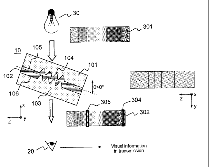
In figure 3A, the component 10, comprising an unstructured metal layer 102
arranged between two dielectric layers 101, 103, is illuminated by a light
source 30, for
example a white light source the spectrum of which is schematically shown by
an array of
colors symbolized by various dotted regions in the chart 301. This may be, for
example, a
spectrum comprising every color in the visible. If an observer 20 observes the
light
transmitted through this component, they receive no visual information.
Specifically, there is
no coupling with a plasmon wave and the metal layer behaves like a reflector.
The incident
light flux is not transmitted by the component.
In the configurations in figures 3B to 3D, a security component 10 with a
structured metal layer 102 forming a corrugated coupling zone 104, such as was
described
above with reference to figures IA and 1B, is considered.
In the example in figure 3B, the observation is carried out at an azimuth of
00
and at normal incidence. The corrugations 104 form a grating for coupling the
incident wave
with surface plasmons supported by the metal/dielectric interfaces 105 and
106, which
grating is optimized at normal incidence for a wavelength given by the
equation (3). At this
3 0
wavelength, the TM component of the incident electromagnetic wave is
transmitted by the
structure remarkably well, and an observer 20 observes colored visual
information
CA 02832477 2013-10-07'
12
corresponding to a thin spectral band about this wavelength. In the spectrum
schematically
showing by the chart 302 in figure 3B, only the light component 303
corresponding to the
spectral band may be seen by the observer.
If an observer continues to observe this same component at an azimuth of 00
but
varies the angle of incidence, they observe a substantial variation in color,
as is shown in
figure 3C. Specifically, as was explained above, a nonzero angle of incidence
(or tilt) 0 of
the y-axis perpendicular to the grating vector causes a large variation in the
coupling
wavelength, both to longer and shorter wavelengths than the coupling
wavelength at normal
incidence. By tilting the component, the observer therefore sees the color
vary greatly with
the angle of tilt. In the example in figure 3C, the references 304, 305 in the
spectrum 302
show the spectral bands seen by the observer.
In the example in figure 3D, the observed component is rotated, not about the
y-
axis, perpendicular to the grating vector, but about the z-axis, parallel to
the grating vector.
In this case, a small variation in the wavelength is observed, illustrated by
the spectral bands
304, 305 in the transmitted spectrum. Indeed, this configuration is equivalent
to the
configuration illustrated in figure 2B in which the component is turned about
an axis parallel
to the grating vector.
Thus it would appear that, depending on the azimuth and tilt, the behavior of
the
transmissive grating will be completely modified, and it is in particular this
effect that the
Applicant has employed to produce a security component that is controllable in
transmission.
Lastly, it is worth noting that the component thus produced may be observed by
an observer from either side, i.e. in the example in figures 3B to 3D, with
either the layer
101 or the layer 103 oriented toward the light source 30, with the same
effect. Specifically,
the dielectric/metal/dielectric structure, comprising dielectric materials of
similar or
comparable refractive indices, is symmetric, and the extra layers which could
be added on
either side, with a view to use of the component, are neutral, as will be
described below.
Figure 4 shows an optical security component 40 according to one embodiment
of the invention. It is a cross section through the metal layer, only one of
the layers of
dielectric being shown. Figures 5A, 5B on the one hand, and 6A, 6B on the
other hand, are
figures or curves showing the transmission calculated for the component in
figure 4
depending on various parameters.
CA 02832477 2013-10-07
13
The component 40 comprises two coupling zones 41, 42, each comprising a set
of corrugations 410, 420 symbolized by dotted strips in figure 4. In this
example, the
corrugations of each coupling zone are oriented in a main direction, defining,
for each
coupling zone, a grating vector, kti and ka2, respectively, pointing in a
direction
perpendicular to the main direction of the corrugations, and of norm given by
kg, = 27r/A,
where AI is the pitch of the corrugations in each of the zones. In this
example, the grating
vectors of the coupling zones are substantially orthogonal. In the orthonormal
coordinate
system x, y, z in figure 4, the corrugations 410 of the coupling zone 41 are
thus oriented
along the z-axis (grating vector pointing along the y-axis), and the
corrugations 420 in the
coupling zone 42 are oriented along the y-axis (grating vector pointing along
the z-axis), the
x-axis being the axis perpendicular to the surface of the component, which is
also the plane
of the figure. In this example, the sets of corrugations 410, 420 have
substantially identical
characteristics (their pitch and the nature of the metal in particular) such
that the central
wavelength is substantially identical for both coupling zones. Alternatively,
one of the
parameters could be modified, for example the pitch of the corrugations, or
the nature of the
metal and the thickness of the layer, in such a way as to modify the central
wavelength, and
therefore the "color" at normal incidence, observed by an observer.
Figures 5A and 5B illustrate the transmission calculated for the coupling
zones
41 and 42, respectively, as a function of angle of incidence measured about
the z-axis, and of
wavelength, when an observer observes the component 40 with an azimuth of 0
under white
light. For these calculations, the same electromagnetic wave propagation
simulating software
package that was used above was used, and the conditions were identical to
those used for
the simulations presented in figures 2A and 2B.
In the coupling zone 41 of the component, the angle of incidence was varied
about an axis perpendicular to the grating vector. A very large variation in
the coupling
wavelength was then observed as a function of angle of incidence (figure 5A).
The
simulation was carried out for the TM mode, the contribution of which was
demonstrated by
the Applicant to be largely dominant over the contribution of the TE mode, and
which
therefore represented what an observer would see under unpolarized light. The
applicant
demonstrated that an angular variation of 1 shifted the TM polarization by 7
nm, whereas
the TE mode was shifted by almost zero. Thus, at normal incidence, an observer
will see a
-1
CA 02832477 2013.-10-07 =
14
green color in transmission corresponding to a spectral band centered on about
560 nm. By
turning the component about the z-axis, the zone 41 will very quickly be seen
to take on a
mainly red and slightly blue tint corresponding to the two coupling
wavelengths associated
with the co-propagating and contra-propagating modes. In the coupling zone 42,
rotation of
the component about the z-axis corresponds to a rotation about an axis
parallel to the grating
vector. Figure 5B shows the variation in transmission as a function of angle
of incidence and
wavelength, calculated for TE mode, the contribution of which, in this
configuration, is
largely dominant over the TM mode. The color variation observed in figure 5B
is much
smaller, and the zone 42 will remain a green tint.
Figures 6A and 6B thus show, for an angle of incidence, to the z-axis (figure
4),
of 0 (curve 602) and 15 (curve 601) respectively, the transmission as a
function of
wavelength in zones 42 (figure 6A) and 41 (figure 6B) respectively, calculated
with the same
parameters as above. These curves confirm the small variation in the
transmission as a
function of wavelength observed in the zone 42 relative to the very large
variation in
wavelength observed in the zone 41. Thus, the central wavelength of the
transmitted spectral
band passes from 615 nm at normal incidence, to 601 nm for an angle of 15 in
the zone 42,
whereas it passes from 615 nm at normal incidence, to 508 nm for an angle of
15 in the
zone 41.
The same observer, if they turned the component about the y-axis (figure 4)
would in contrast see a very large variation in the color of the coupling zone
42, of the type
shown in figure 5A, calculated for TM mode, and a very small variation in the
color of the
coupling zone 41, as is illustrated in figure 5B, calculated for TE mode.
Thus, by varying the angle of incidence of the component about one or other of
the axes, it will be possible for an observer to see the color of one of the
zones vary very
rapidly whereas the color of the other zone will remain fairly stable.
Advantageously, the orthogonality of the coupling gratings formed by the sets
of
corrugations 410 and 420 is respected to within 5 . This is because the
Applicant has
demonstrated that in this range of variation in the angle between the two sets
of corrugations,
a very good color stability will continue to be perceived in the coupling zone
the grating
vector of which is parallel to the axis of rotation of the component, and the
variation in the
coupling wavelength will be equally as effective in the coupling zone the
grating vector of
CA 02832477 2013-10-07
which is perpendicular to the axis of rotation of the component. If the
orthogonality of the
two sets of corrugations differs by more than the threshold of about 5 , the
effect will be
less and less visible, because the contrast between the coupling zone in which
the color is
stable and the coupling zone in which the color rapidly varies will be
smaller.
5
Advantageously, the zones 41, 42 in figure 4 could be given complementary
shapes and characteristics, as is illustrated, for example, in figures 7A to
7D. Figure 7A is a
cross-sectional view of an example security component 70, through the metal
layer 102.
Figures 7B to 7D illustrate the component 70 as seen in transmission in
various
configurations.
10 As may
be seen in figure 7A, one coupling zone 72, comprising a set of
rectilinear and parallel corrugations forming a coupling grating of grating
vector kg2, has a
heart shape. The coupling zone 71 comprises substantially rectilinear and
parallel
corrugations arranged in a direction perpendicular to that of the corrugations
of the coupling
zone 72 in order to form a coupling grating of grating vector kgi, and its
shape is
15
complementary to that of the coupling zone 71. Thus, in this example, the
coupling zone 71
has a substantially rectangular shape, its corrugations being interrupted in a
central zone
corresponding to the coupling zone 72. Moreover, the security component shown
in figure
7A comprises a zone 73 that forms a frame about the coupling zone 71, and in
which the
metal layer is not structured.
If an observer observes the security component 70 in transmission at normal
incidence, they will see an image of the type shown in figure 7B, i.e. having
a uniform color
over the entire component (if the parameters of the sets of corrugations are
substantially
identical) except in the unstructured zone 73, which for its part has a
constant optical density
that is clearly higher than those of the structured zones 71, 72. The color
will be that
corresponding to a spectral band centered on the wavelength at which the
grating formed by
the corrugations is optimized, for example a green color at about 550 nm, as
in the preceding
example.
If the observer rotates the component 70 about an axis perpendicular to the
grating vector kg' (figure 7C), they will observe a rapid variation in the
color of the coupling
zone 71, whereas the color of the heart-shaped coupling zone 72 will remain
stable. If in
contrast, the observer rotates the component 70 about an axis perpendicular to
the grating
CA 02832477 2013-10-07'
16
vector kg2 (figure 7D), they will observe a rapid variation in the color of
the heart-shaped
coupling zone 72, whereas the color of the coupling zone 71 will remain
stable. Thus,
rotation of the component about one axis induces a rapid variation in the
color of one of the
zones, which corresponds in this example to a pattern of characteristic shape,
whereas
rotation about the perpendicular axis induces a rapid variation in the
complementary zone.
An observer will easily be able to verify the authenticity of a document of
value
secured by virtue of the various levels of security provided by such a
component. It will be
sufficient for them to observe the component in transmission under unpolarized
white light.
By varying the angle of observation of the component in tilt about one of the
axes of the
pattern, they will observe a rapid variation in the color of one zone. This
variation will be all
the more characteristic because, in a complementary zone, the color varies
very little.
Moreover, the presence of an unstructured, and therefore opaque, reference
zone (zone 73 in
the example in figure 7) highlights the transparency of the coupling zones.
For a second level
of verification, it will be possible to vary the angle of incidence of the
component about an
axis perpendicular to the first axis. The observer will then observe a rapid
variation in the
color of the zone that is complementary to the first.
Figures 8 and 9 illustrate two variants of a security component according to
the
invention, their coupling zones having grating vectors that are perpendicular
pairwise.
Figures 8A and 8B illustrate security components comprising corrugations 800
arranged concentrically. The corrugations 800 may be polygonal (figure 8A) or
circular
(figure 8B) in shape. A plurality of coupling zones, referenced 801 to 808,
may be defined,
each of which contains corrugation portions that are substantially rectilinear
and parallel,
forming coupling gratings defined by grating vectors ko to ligs.
If an observer observes a security component 80 of the type thus described in
transmission at normal incidence, they will see a dot 810 of a uniform color
(figure 8C)
defined by the spectral band about the wavelength at which the coupling
gratings are
optimized. This color therefore depends on the pitch and the depth of the
corrugations 800,
and on the thickness of the metal layer. If an observer tilts the component,
i.e. makes the
angle of incidence vary, coupling zones 811 having grating vectors
perpendicular to the
rotation axis of the component (coupling zones symmetric about the center of
symmetry of
the component) will see their colors vary very rapidly, whereas the color of
the rest of the
CA 02832477 2013-10-07'
17
dot (812, figure 8C) will remain stable.
Because of the axial symmetry of the component about the x-axis in figure 1A,
it will be possible, whatever the azimuthal orientation of the component, to
observe a
variation in color in two symmetrical zones of the component by rotating the
latter about an
axis contained in the plane of the component (tilt). Moreover, for a given
azimuth, by
varying the axis of rotation of the component, the color in other zones of the
component,
corresponding to two symmetric zones for which the grating vector is
substantially
perpendicular to the axis of rotation, will be observed to vary, again making
the security
component very easy to authenticate.
Figure 9A schematically shows a security component 90 that is also axially
symmetric, which component 90 has corrugations arranged radially (not shown in
figure 9A)
such that coupling zones containing substantially rectilinear and linear
corrugations could be
defined locally, the corrugations in each zone defining a grating vector kg;
pointing in a
direction perpendicular to the main direction of the corrugations in the zone.
Here again, as illustrated in figure 9B, an observer observing the sample in
transmission at normal incidence will see a substantially uniform color
corresponding to the
coupling wavelength defined by the pitch and the depth of the corrugations. By
tilting the
component, they will observe a rapid variation in the color in symmetric zones
the grating
vectors of which are perpendicular to the rotation axis of the component. As
was the case for
the component described in figure 8, the effect will be insensitive to the
azimuthal position
of the component due to its axial symmetry, and a rotation about a different
axis will lead to
a variation in the color in another zone of the component.
Security components such as described above may be produced in the following
way. The optical structures (corrugations) of the various zones are written,
by
photolithography or e-beam lithography, into a photoresist. An electroplating
step allows
these optical structures to be transferred to a resistant material, for
example a nickel-based
material, in order to produce a "master". The master is then used in a
stamping step in order
to transfer the microstructure to a film and to structure the dielectric layer
101 (figure 1A),
typically an embossing lacquer a few microns in thickness borne by a polymer
film that is 12
gm to 50 pm in thickness, for example a polyethylene terephthalate (PET) film.
The
stamping may be carried out by hot embossing or casting the dielectric. The
refractive index
CA 02832477 2013-10-07.
18
of the layer formed of the embossing lacquer is typically 1.5. Next, the layer
thus stamped is
metallized. The metallization is carried out under vacuum in a way that allows
its thickness
to be perfectly controlled, and with one, for example, of the following
metals: silver,
aluminum, gold, chromium, copper, etc. A sealing layer of controlled
refractive index is then
applied, for example using a coating process. For certain applications, such
as products for
lamination or hot-marking, this layer may be the adhesive layer. The sealing
layer, which
forms the layer 103 (figure 1A) has a refractive index substantially the same
as that of the
embossed layer, about 1.5, and the thickness larger than several microns.
Depending on the
intended final application of the product, an adhesive may be applied to the
sealing layer.
As a variant, it is possible for a number of different metals to be applied in
the
metallization step, for example in order to produce different visual effects.
To do this, it is
for example possible to apply, with a given pattern, a soluble ink to the
embossed layer.
During the metallization with the first metal, the latter is applied uniformly
over the layer
but, once the ink has been removed, remains in place only in zones that were
free from ink.
Next, a selective second metallization is carried out, also comprising a
selective prior step of
printing with a soluble ink, allowing the zones where the second metal will be
applied to be
selected. It is possible, during the application of the second metal, for the
metal layers to be
superposed locally, forming zones of higher optical density, or in contrast
for non-metallized
zones to result, which zones, once covered by the sealing layer, will form
transparent zones
in the component.
As a variant, the different metal zones may correspond to different coupling
zones. In other words, the first metal is applied to one or more first
coupling zones, whereas
the second metal is applied to one or more second coupling zones, allowing
distinct color
effects to be obtained in the various coupling zones. Alternatively, the
various metals may be
deposited in zones that do not correspond to coupling zones.
Advantageously, the most opaque zones, which require at least 2
metallizations,
or in contrast the most transparent zones, which may from the first partial
metallization
= onward, will possibly be used to form graphical elements separating the
zones formed of the
various metals. These elements will be used by those skilled in the art to
reinforce the impact
of the design in order to make it easier for the person responsible for
checking to read it.
Figure 10 schematically shows a (partial) cross-sectional view of the
component
CA 02832477 201.3-10-07'
19
thus obtained. Only the functional layers required to obtain the plasmonic
effect are shown
in this figure. Optional supporting or adhesive films are not shown. The two
metal layers
108, 109 are located between the dielectric layers 101 and 103. The zone 107
represents the
zone where the layer 103 is embossed and the metal layers structured, i.e. the
zone in which
the corrugations (not shown) are found. As a variant, the various metals will
possibly
correspond to various coupling zones. Due to the different nature of the
metals used, the
different zones of such a component will possibly exhibit different color
effects, both when
the reflected color of the material is observed and when plasmonic waves are
observed in
transmission. Specifically, the "plasmonic" color of a grating results from
the grating and the
nature of the metal layer. Moreover, as it is more complicated to produce,
such a product
potentially has a much higher resistance to counterfeiting.
As will have been apparent from the example manufacturing method described
above, inclusion of an optical security component according to the invention
in a secure
document is perfectly compatible with the presence in the same document of the
grating-
based structures conventionally used to produce holographic components.
In particular, it will be possible to produce an optical security element
comprising one or more plasmonic components of the type described above and
one or more
other types of optical security components, holograms for example.
To do this, a master will possibly be produced by writing the various
patterns,
corresponding to the various optical security components, into the photoresist
and then
electroplating said patterns. Next, the stamping step may be carried out using
the master to
transfer the various microstructures into the polymer film intended to be
embossed. The
metallization the thickness of which must be controlled for the plasmonic-
effect components
may be carried out over the entire film, because it will not adversely affect
the other DOVID
components, which function in reflection.
Figures 1 IA to 11C show a secure document 1, for example a document of
value of the banknote type, thus equipped with a security element 110
comprising a
plasmonic optical security component 70 and other optical security components
111,
holographic components for example. Figure I lA shows a top view of this
component,
figure 11B shows a bottom view and figure 11 C a cross-sectional view.
The security element 110 takes the form of a strip, typically 15 mm in width,
CA 02832477 2013-10-07
which is fastened to a support 112 of the document 1. The security element 110
is fastened
to the support 112 by known means. For example, in the case of a document
containing a
transparent solid zone, the security element may be fastened by hot transfer
with activation
of a transparent adhesive layer applied beforehand to the sealing layer 101.
In this case, a
5 detachment layer (for example a wax layer) may be applied between the
embossing lacquer
103 and the supporting PET film (not shown in figure lA or figure 10). The
security element
is transferred to the document by pressing the hot security element against
the document, the
plasmonic component being located facing the transparent zone. During the
transfer, the
adhesive film bonds to the support 112 of the document and the detachment
layer and the
10 supporting film are removed. A transparent window 113 is provided in the
support 112 level
with the plasmonic component 70. Seen from above, all the optical security
components will
be visible on the secure document 1 and it will be possible to check them all
using various
prior-out methods. Seen from below, only the one or more plasmonic components
will be
visible; it will be possible to check them in transmission, as was described
above.
15 Figures 12A and 12B illustrate cross-sectional views of two variants
of an
embodiment of a secure document 1 equipped with a security element comprising
an optical
security component 120. In these two examples, the optical security component,
or the
optical security element bearing the optical security component, is
encapsulated in the
support 122 of the secure document. In the example in figure 12 A, the secure
document 1 is
20 for example obtained by laminating a number of layers 125, 126, 127, the
optical security
component being integrated into the middle layer 126, whereas transparent
zones 123, 124
are provided in the external layers 123, 124 in order to ensure the optical
security component
120 can be seen. As a variant, the layers 125, 126, 127 may be combined in
order to form a
uniform support 122 in which the optical security component is encapsulated.
In the example
in figure 12B, the optical security component is fixed to a first layer 122
forming a support,
the assembly being with covered with a layer 124 made of a transparent
material. A
transparent window 123 is provided in the supporting layer 122 in order to
allow the optical
security component 120 to be observed in transmission. This transparent window
may be a
gap or a locally transparent material. The document 1 thus produced is for
example a
security document such as an identity card or a banknote equipped with a
security thread.
The secure document thus obtained can be very easily checked by an
CA 02832477 2013-10-07'
=
21
inexperienced user, and the authentification obtained is highly reliable. As
has been shown,
the plasmonic optical security component according to the invention will
possibly take the
form of a security film the characteristics of which may be checked by eye in
the visible.
Visual authentication of the secure document is therefore possible, including
under natural
light. This authentication, based on visual effects that differ in
transmission depending on
the rotation axis of the component, is particularly easy to carry out.
In practice, an observer will possibly check the secure document by observing
the plasmonic component in transmission in front of a white light source.
Alternatively, it
will be possible to check the security component by placing it in a light-
emitting support.
Although described by way of a certain number of embodiments, the optical
security component according to the invention and the method for manufacturing
said
component comprise various variants, modifications and improvements that will
appear
obvious to those skilled in the art, it being understood that these various
variants,
modifications and improvements form part of the scope of the invention such as
defined by
the following claims.