Note: Descriptions are shown in the official language in which they were submitted.
CA 02832915 2015-06-25
TRANSPORT OF MULTIPLE ASYNCHRONOUS DATA STREAMS
USING HIGHER ORDER MODULATION
[0001]
BACKGROUND OF THE INVENTION
1. Field of the Invention
[0002] The present invention is generally related to
optical transport systems. More particularly, aspects of the
present invention are directed to transportation of multiple
asynchronous data streams over an optical transport system
using high order modulation.
2. Description of Related Art
[0003] A number of existing networking scenarios involve
the transporting of a number of data streams from routers or
switches over various geographical areas, such as across a
metropolitan area or a regional network, in a manner that
optimizes the uses of available optical fiber spectrum. The
incoming data streams are typically asynchronous, typically
out of phase and with clock rates within +/- 100ppm, as they
may arrive from different, independent sources.
[0004] Some solutions employ time division multiplexing
("TDM"), for instance using a Synchronous Optical NETwork
("SONET")/ Synchronous Digital Hierarchy ("SDH") or Optical
Transport Network ("OTN") hierarchy in which the lower speed
services are synchronously multiplexed to a higher data rate
for transmission. Other solutions employ Wavelength Division
Multiplexing ("WDM"), where different incoming data streams
are mapped to different wavelengths and then multiplexed on to
a single fiber.
[0005] In TDM, the incoming asynchronous data streams are
mapped to transport containers which are then TDM multiplexed
- 1 -
CA 02832915 2013-10-10
WO 2012/145165 PCT/US2012/032055
to create a higher speed container. This higher
speed
container (stream) is then transmitted using a variety of
optical modulation techniques ranging from simple on-off
keying to high-order modulation based on phase and
polarization. However, TDM
is limited by the fastest
electronic transmitting, receiving, channel impairment and
processing technology available. Therefore,
important
deficiencies of TDM-only transport include the cost,
complexity and power consumption burdens of the TDM
multiplexing stage and subsequent de-serialization. In
general, the TDM aggregation approach may introduce additional
muitiplexing/demultiplexing complexity as well as the cost
premium of higher speed optics and electronics.
[0006] On the other
hand, if conventional WDM technology
(including Dense WDM "DWDM") is used to transport these lower-
speed asynchronous signals, the spectral efficiency is very
low. Hence, the
full transmission capacity of the fiber may
not be utilized.
SUMMARY OF THE INVENTION
[0007] Aspects of the invention address the cost and
complexity issues of high-speed electronics and optics
associated with a TDM approach and the spectral inefficiency
of WDM with a lower-speed signals approach. As explained
herein, it is possible to maintain a low baud rate for low
cost optics and electronics while enabling a high bit rate for
high spectral efficiency.
[0008] Embodiments
of the invention provide high order
modulation, such as phase and/or amplitude modulation to
achieve multiple bits per symbol, for transport of multiple
data streams in an optical transport system. Supplemental
multiplexing techniques such as time division multiplexing,
polarization multiplexing and sub-carrier multiplexing may
also be used in conjunction with the high order modulation.
This may be done in various combinations to realize a highly
spectrally efficient multi-data stream transport mechanism.
-2-
CA 02832915 2013-10-10
WO 2012/145165 PCT/US2012/032055
[0009] According to
one embodiment, an optical transmitter
system comprises at least one module for performing unframing
by removing framing information from a plurality of N
asynchronous data streams and for synchronizing the
asynchronous data streams. The system also comprises at least
one module for re-framing the synchronized data streams and
for tagging the synchronized data streams with encoded stream
information. The system also comprises a high order modulator
operable to perform 2N level optical modulation of the tagged
synchronized data streams prior to transmission of the tagged
synchronized data streams to an optical receiver.
[0010] In one
example, the system further comprises a
differential encoder for receiving the synchronized data
streams from the at least one re-framing and tagging module.
The differential encoder is operable to encode at least one of
phase and amplitude of signals associated with the
synchronized data streams prior to the high order modulator
performing the 2\ level optical modulation.
[0011] In another
example, the system further comprises a
multiplexer for performing at least one of polarization
multiplexing, sub-carrier multiplexing and time division
multiplexing of the tagged synchronized data streams.
[0012] In one
alternative, the at least one unframing and
synchronizing module comprises a first set of unframing and
synchronizing modules for operating on a first set of the
asynchronous data streams to produce a first set of
synchronous data streams and a second set of unframing and
synchronizing modules for operating on a second set of the
asynchronous data streams to produce a second set of
synchronous data streams. Here, the at least one re-framing
and tagging module comprises a first set of re-framing and
tagging modules for operating on corresponding ones of the
first set of synchronous data streams to produce a first set
of the tagged synchronous data streams and a second set of re-
framing and tagging modules for operating on corresponding
ones of the second set of synchronized data streams to produce
-3-
CA 02832915 2013-10-10
WO 2012/145165 PCT/US2012/032055
a second set of the tagged synchronized data streams. The
high order modulator comprises a first high order modulator
for performing the 2N level optical modulation on the first set
of the tagged synchronized data streams to produce a first
optically modulated signal and a second high order modulator
for performing the 2N level optical modulation on the second
set of the tagged synchronized data streams to produce a
second optically modulated signal. And the
multiplexer is
operable to receive the first and second optically modulated
signals and perform the polarization multiplexing thereon to
generate a single multiplexed optical signal prior to
transmission to the optical receiver.
[0013] In another
alternative, the at least one
unframing and synchronizing module comprises a first set of
unframing and synchronizing modules for operating on a first
set of the asynchronous data streams to produce a first set of
synchronous data streams and a second set of unframing and
synchronizing modules for operating on a second set of the
asynchronous data streams to produce a second set of
synchronous data streams. Here, the at least one re-framing
and tagging module comprises a first set of re-framing and
tagging modules for operating on corresponding ones of the
first set of synchronous data streams to produce a first set
of the tagged synchronous data streams and a second set of re-
framing and tagging modules for operating on corresponding
ones of the second set of synchronized data streams to produce
a second set of the tagged synchronized data streams. The
high order modulator comprises a first high order modulator
for performing the 2\1 level optical modulation on the first set
of the tagged synchronized data streams to produce a first
optically modulated signal and a second high order modulator
for performing the 2N level optical modulation on the second
set of the tagged synchronized data streams to produce a
second optically modulated signal. And the
multiplexer is
operable to receive the first and second optically modulated
signals and perform the sub-carrier multiplexing thereon to
-4-
CA 02832915 2013-10-10
W02012/145165 PCT/US2012/032055
generate a single multiplexed optical signal prior to
transmission to the optical receiver.
[0014] In a further
alternative, the at least one unframing
and synchronizing module comprises a plurality of unframing
and synchronizing modules, each of the plurality of unframing
and synchronizing modules being configured to operate on a
corresponding set of the asynchronous data streams to produce
a corresponding set of synchronous data streams. The at least
one re-framing and tagging module comprises a plurality of re-
framing and tagging modules. Each of the
plurality of re-
framing and tagging modules is configured to operate on a
corresponding one of the of synchronous data streams to
produce a corresponding tagged synchronous data stream. Here,
the multiplexer comprises a plurality of time division
multiplexers. Each of the
time division multiplexers is
operable to multiplex a set of the tagged synchronous data
streams and generate a time division multiplexed signal. And
the high order modulator is operable to receive the time
division multiplexed signals from the plurality of time
division multiplexers and to perform the 2" level optical
modulation thereon.
[0015] In another
example, the system further comprises a
plurality of optical to electrical converters for converting
the N asynchronous data streams from optical signals to
electrical signals prior to the at least one module performing
the unframing and synchronizing on the asynchronous data
streams. In a further example, the system further comprises a
wavelength division multiplexer for multiplexing a signal from
the high order modulator with one or more other optical
signals prior to transmission to the optical receiver. And in
yet another example, the high order modulator is operable to
perform the 2\ level optical modulation using phase shift
keying or quadrature amplitude modulation.
[0016] In
accordance with another embodiment, a method of
optically transmitting data comprises receiving a plurality of
N asynchronous data streams; performing unframing on each of
-5-
CA 02832915 2015-06-25
the plurality of N asynchronous data streams; synchronizing
the plurality of N asynchronous data streams; reframing and
tagging the synchronized data streams to map the data into a
structured transmission frame including a tag to identify one
or more specific ones of the data streams with encoded stream
information; and performing 211 level optical modulation of the
reframed and tagged synchronized data streams to produce a
high order modulated signal configured for transmission to an
optical receiver.
[0017] In one example, the method further comprises
differential encoding the synchronized data streams with at
least one of phase and amplitude of signals associated with
the synchronized data streams prior performing the 2" level
optical modulation.
[0018] In another example, the method further comprises
performing multiplexing of the reframed and tagged
synchronized data streams. Here, the multiplexing includes at
least one of polarization multiplexing, sub-carrier
multiplexing and time division multiplexing.
[0019] In one alternative, the unframing and synchronizing
produces a first set of synchronous data streams and a second
set of synchronous data streams; the reframing and tagging
produces a first set of the reframed and tagged synchronous
data streams from the first set of synchronous data streams
and a second set of the reframed and tagged synchronized data
streams from the second set of synchronous data streams; the 2N
level optical modulation includes performing high order
modulation on the first set of the reframed and tagged
synchronized data streams to produce a first high order
modulated signal and performing the high order modulation on
the second set of the tagged synchronized data streams to
- 6 -
CA 02832915 2015-06-25
produce a second high order modulated signal; and the
multiplexing includes performing the polarization multiplexing
on the first and second high order modulated signals to
generate a single multiplexed optical signal prior to
transmission to the optical receiver.
- 6a -
CA 02832915 2013-10-10
WO 2012/145165 PCT/US2012/032055
[0020] In another alternative, the unframing and
synchronizing produces a first set of synchronous data streams
and a second set of synchronous data streams; the reframing
and tagging produces a first set of the reframed and tagged
synchronous data streams from the first set of synchronous
data streams and a second set of the reframed and tagged
synchronized data streams from the second set of synchronous
data streams; the 2 level optical modulation includes
performing high order modulation on the first set of the
reframed and tagged synchronized data streams to produce a
first high order modulated signal and performing the high
order modulation on the second set of the tagged synchronized
data streams to produce a second high order modulated signal;
and the multiplexing includes performing the sub-carrier
multiplexing on the first and second high order modulated
signals to generate a single multiplexed optical signal prior
to transmission to the optical receiver.
[0021] In a further alternative, the unframing and
synchronizing produces a first set of synchronous data streams
and a second set of synchronous data streams; the retraming
and tagging produces a first set of the reframed and tagged
synchronous data streams from the first set of synchronous
data streams and a second set of the reframed and tagged
synchronized data streams from the second set of synchronous
data streams; the multiplexing includes performing a first
time division multiplexing operation on the first optically
modulated signal to generate a first time division multiplexed
signal and performing a second time division multiplexing
operation on the second optically modulated signal to generate
a second time division multiplexed signal; and the 2N level
optical modulation includes performing the 2N optical
modulation on the first and second time division multiplexed
signals.
[0022] In another example, the method further comprises
converting the N asynchronous data streams from optical
signals to electrical signals prior to performing the
-7-
CA 02832915 2013-10-10
M4) 2012/145165 PCT/US2012/032055
unframing and synchronizing. In yet
another example, the
method further comprises performing wavelength division
multiplexing on the high order modulated signal with one or
more other optical signals prior to transmission to the
optical receiver. And in another example, the 2' level optical
modulation employs phase shift keying or quadrature amplitude
modulation.
[0023] In a further
embodiment, an optical transceiver
comprises at least one module for performing unframing by
removing framing information from a plurality of N
asynchronous data streams and for synchronizing the
asynchronous data streams. The transceiver also comprises at
least one module for re-framing the synchronized data streams
and for tagging the synchronized data streams with encoded
stream information and a high order modulator operable to
perform 2N level optical modulation of the tagged synchronized
data streams prior to transmission of the tagged synchronized
data streams to an optical receiver. The transceiver further
comprises an optical receiver module operable to receive
tagged synchronized data streams from a remote high order
modulator and perform at least one of demodulation and
detection on the received tagged synchronized data streams to
output a received set of streams, a decoder operable to decode
the received set of streams to generate decoded streams, and
at least one module for re-framing the decoded streams.
[0024] In one
example, the optical transceiver further
comprises means for performing tag identification and
reordering on the decoded streams prior to re-framing thereof.
In another example, the optical transceiver further comprises
means for performing signal conditioning on the received set
of streams to clean up transmission impairments in the
received set of streams. In yet another example, the optical
receiver module is operable to perform direct detection with
balanced photodetectors to extract differential phase
information from the received tagged synchronized data
streams. And in another example, the optical receiver module
-8-
CA 02832915 2013-10-10
M4)2012/145165 PCT/US2012/032055
includes one or more local oscillators operable to perform
coherent detection to extract phase states from the received
tagged synchronized data streams.
BRIEF DESCRIPTION OF THE DRAWINGS
[0025] FIG. 1 illustrates an exemplary optical transceiver
architecture in accordance with one aspect of the invention.
[0026] FIG. 2 illustrates conversion of multiple
asynchronous data streams to synchronous streams in accordance
with aspects of the invention.
[0027] FIG. 3 illustrates the use of polarization and sub-
carrier multiplexing with high-order modulation in accordance
with aspects of the invention.
[0028] FIG. 4 illustrates time division multiplexing with
high-order modulation in accordance with aspects of the
invention.
[0029] FIGS. 5A-B illustrate exemplary high-order
modulation constellations for use with aspects of the
invention.
[0030] FIG. 6 illustrates one method of frame
identification using an embedded tag in accordance with an
aspect of the invention.
[0031] FIG. 7 illustrates a second method of frame
identification using an embedded tag in accordance with
another aspect of the invention.
[0032] FIG. 8 illustrates a system using 16-QAM high order
modulation in accordance with an aspect of the invention.
[0033] FIG. 9 illustrates an exemplary square 16-QAM
transmitter configuration in accordance with an aspect of the
invention.
[0034] FIG. 10 illustrates
an exemplary star 16-QAM
transmitter configuration in accordance with an aspect of the
invention.
[0035] FIG. 11 illustrates exemplary transmitter and
receiver operation in accordance with aspects of the
invention.
-9-
CA 02832915 2013-10-10
W02012/145165 PCT/US2012/032055
DETAILED DESCRIPTION
[0036] The aspects,
features and advantages of the present
invention will be appreciated when considered with reference
to the following description of embodiments and accompanying
figures. The same reference numbers in different drawings may
identify the same or similar elements. Furthermore, the
following description does not limit the present invention;
rather, the scope of the invention is defined by the appended
claims and equivalents.
[0037] As presented
herein, optical systems according to
embodiments of the invention use high order modulation to
transmit multiple bits per symbol. Such systems
may employ
differential encoding with a data stream identifier to recover
data streams at a receiver. As will be
explained in more
detail below, either direct detection using balanced receivers
or coherent detection using an optical local oscillator may be
used by the receiver.
[0038] FIG. 1 is a
block diagram illustrating an optical
transceiver system 100 according to aspects of the invention.
The system 100 employs multiple lower speed client signals on
the input side, and a higher speed signal on a DWDM wavelength
on the output side. As shown in this embodiment, a plurality
of N asynchronous data streams is input to the system 100.
The N data streams may each be of a slightly different data
rate, for instance with each stream at a given data rate of R
gigabit/sec, typically within +/- 100 ppm difference. The N
streams are passed through payload level un-framing modules
102 and synchronized at synchronization block 104. The un-
framing modules 102 remove Infiniband, Ethernet or SONET
framing. The data
streams are aligned with synchronization
block 104. For transmission scenarios employing
synchronization, synchronization block 104 enables all streams
to be re-timed from the same reference clock such that they
are all transmitting at the same data rate. The un-
framing
and synchronization may be done separately or concurrently in
-10-
CA 02832915 2013-10-10
VM) 2012/145165 PCT/US2012/032055
the same or different equipment. Prior to
reception by the
un-framing modules 1021 - 102N, the data streams may be
converted from optical to electrical signals via converter
modules 1051 - 105N. These
converter modules 105 may be
omitted if the incoming streams are received as electrical
signals instead of optical signals.
[0039] Subsequently,
the streams are re-framing with one or
more framing modules 106 and tagged at block 108 to recover
the data of the streams. The framing
modules 106 add
information such as a header or marker to the stream, and
tagging block 108 encodes stream information. The reframing
and tagging may be done separately or concurrently in the same
or different equipment. The framing
and tagging sections
perform the function of mapping the incoming client data into
a structured transmission frame of fixed size and adds header
information. As part of
this header information, a tag is
added to identify a specific client stream. This tag is used
to recover that client stream at the receiver location.
[0040] The streams are then desirably provided to a
differential encoder 110, which encodes the phase and/or
amplitude of the signals. Desirably, the differential
encoding is performing using a data stream identifier to
enable recovery of the data streams at the receiver. The data
stream identifier may be a simple 3 or 4 bit binary code,
e.g., 100 or 1011. The
differentially encoded signals are
then sent to an optical modulator complex 112. Here, the data
of the individual streams is mapped to multiple constellation
points, for example using gray coding, on an n-level
modulation signal. Each of these constellations (representing
a combination of amplitude and phase modulation) are modulated
on a carrier wave generated by continuous wave (CW) laser 114,
and multiple instances of these modulated optical signals are
multiplexed together for transmission over a DWDM wavelength
via a fiber optic cable.
[0041] In one
example, the high order modulation uses 16
QAM to transmit 4 bits/symbol. In this
example, the symbol
-11-
CA 02832915 2013-10-10
WO 2012/145165 PCT/US2012/032055
(baud) rate may be 10 Gb/s with a bit rate of 40 Gb/s. This
allows for transmission of four asynchronous 10 Gb/s data
streams with a single WDM wavelength, and using a 50 GHz
wavelength grid. Thus, the system is able to maintain a low
baud rate while enabling a high bit rate for high spectral
efficiency. In other
examples as explained below, the high
order modulation may be used in combination with one or more
additional modulation schemes. These
include polarization
multiplexing, sub-carrier multiplexing and intermediate TDM
multiplexing.
[0042] On the
receiver side as shown in FIG. 1, the DWDM
signals are input to an optical receiver module 116, which
functions as a demodulator and/or detector. It converts
the
optical signals to electrical signals. In one
example, the
receiver module 116 may perform direct detection with balanced
photodetectors to extract differential phase information. In
another example, the receiver module 116 may employ local
oscillator based coherent detection with an optical hybrid to
extract phase states. The module
116 may be used with or
without a digital signal processor ("DSP") back end for signal
clean up.
[0043] A signal
conditioner 118 may be included as part of
system 100. If it is
included, the signal conditioner 118 is
used to clean up transmission impairments such as dispersion,
compensating for the impairments after the signal
has traversed the length of fiber. The signal conditioner 118
desirably includes compensation for chromatic dispersion,
e.g., using Finite Impulse Response ("FIR") filters or maximum
likelihood sequence estimators (MLSE), and phase and
polarization recovery. This is achieved using known adaptive
equalization algorithms. The
resultant streams are decoded
with decoder 120. Reframing is done by individual reframing
modules 1221 - 122N. At this time, tag identification and/or
reordering is accomplished at block 124. Tag
identification
and reordering (if necessary), can be performed before the
reframing process takes place. The
reframing, tagging and
-12-
CA 02832915 2013-10-10
VM10 2012/145165 PCT/US2012/032055
reordering may be done separately or concurrently in the same
or different equipment. Then electrical to optical converter
modules 1261 - 126N may be used to convert the signals back
into N optical data streams, which are passed onto downstream
equipment (not shown). Alternatively, the optical converter
modules 126 may be omitted when electrical signals are send to
the downstream system.
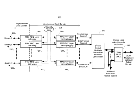
[0044] In accordance
with the above discussion, FIG. 2
illustrates an exemplary system 200 for transporting multiple
asynchronous data streams 2021 - 202N as an optical signal with
high order modulation. The figure
shows wavelength
multiplexing of multiple modulated signals (N streams) before
transmission over an optical fiber. The
separation between
the asynchronous and the synchronous clock domains is achieved
through remapping (e.g., unframing as shown in blocks 204_ -
204N) of the asynchronous data streams into PHY and/or MAC
layer frames and then reframing them synchronously (e.g.,
framing and tagging as shown in blocks 2061 - 206N) using a
common reference clock 208 as the synchronous reference.
[0045] The
synchronous data streams are then modulated with
multi-level modulation and multiplexed at block 210, for
instance as explained with regard to modulator complex 112 of
FIG. 1. For N synchronous bit streams, a 2N symbol modulation
scheme is used such that each of the synchronous streams can
be treated as one bit in a N-bit symbol that is then mapped
into 2N symbol modulated stream. Each of those
modulated
stream can be carried on a pre-specified carrier wavelength
for further multiplexing in the wavelength domain. Additional
multiplexed optical signals may be added to the WDM
multiplexed signals prior to transmission, as shown in block
212. The reverse
process is employed on received signals to
obtain the asynchronous data streams 2021 - 202N.
[0046] As explained
above, additional modulation schemes
may be employed along with high order modulation. FIG. 3
provides an exemplary architecture 300, which combines high
order modulation with a second orthogonal multiplexing method
-13-
CA 02832915 2013-10-10
M4) 2012/145165 PCT/US2012/032055
(e.g., polarization or sub-carrier multiplexing). In this
embodiment, the clock domains for the polarization or sub-
carrier multiplexing can be completely independent. For
instance, as shown there are two sets of streams (11 - 1N and
21 to 2N) processed by respective blocks 3021 and 3022. Upon
completion of the unframing processing, the upper set of
streams (11 - 1N) has a first common clock 3041 and the lower
set of streams (21 to 2N) has a second common clock 3042. The
first and second common clocks are desirably independent of
one another. For
instance, the clocks may be selected on a
per-line card basis. Each line card typically represents one
or two wavelengths.
[0047] The transmit
and receive processing of the stream
sets shown in FIG. 3 may proceed as discussed above with
regards to FIGS. 1 and 2, subject to the further multiplexing
as discussed below. On the
transmit side, once the separate
stream sets (12 - 1N and 21 to 2N) have been processed by their
respective optical modulator complexes 3061 and 3062, which
function as block 210 in FIG. 2 and the optical modulator
complex 112 in FIG. 1, they are multiplexed together in block
303, for instance either by polarization multiplexing or sub-
carrier multiplexing. Polarization
multiplexing may be done
using a Polarization Beam Combiner ("PBC"). Subcarrier
multiplexing may be done with an FPGA or ASIC or other
mechanism by which a comb of sub-carriers (typically spaced
much closer than the DWDM grid) are multiplexed using a series
of modulators and SF combined and followed by a RE-to-optical
upconverter to modulate the laser source. The
resultant
output from block 308 is a single multiplexed optical signal
that is then sent to a WDM multiplexer 310. Here, as with WDM
multiplexer 212, additional multiplexed optical signals may be
added and the resultant optical stream is ready for
transmission via an optical cable (not shown). On the
receiving side, the reverse processing occurs, where the input
from the optical cable is WDM demultiplexed and any additional
-14-
CA 02832915 2013-10-10
M/02012/145165 PCT/US2012/032055
multiplexed optical signals are removed prior to polarization
or sub-carrier demultiplexing.
[0048] Sub-carrier
multiplexing in the present embodiment
may employ co-carriers or multiple carriers. With sub-carrier
modulation, an additional set of transmitters and receivers
are used, but the composite optical spectrum can be
transmitted through a single ITU grid window, making It more
spectrally efficient. The total number of data streams
supported increases by a factor equal to the number of sub-
carriers (e.g., 2).
[0049] FIG. 4 shows
an exemplary system 400 that includes a
combination of high-order modulation with an intermediate TDM
multiplexing stage. In this
embodiment, the TDM stage
synchronously multiplexes the two incoming streams using a
common clock. As shown, the
system 400 is arranged in a
similar manner to system 200 of FIG. 2. Here, different sets
(e.g., pairs) of asynchronous streams 4021, 4022, ..., 402N are
processed by unframing modules 404 and framing/tagging modules
406 using timing from a common local clock 408 to become
corresponding pairs of synchronous streams. Prior to
modulating with multi-level modulation at block 410, each
synchronous stream pair is time division multiplexed at
respective block 412 to produce a multiplexed signal.
[0050] The
intermediate TDM multiplexing stage (blocks 4121
- 412N) increases the data rate to enable more incoming data
streams to be supported. For example, using only high-order
modulation, a constellation size of 2N with a symbol rate of R
supports N streams each operating at a data rate of R. With
the use of the intermediate TDM stage in this embodiment, the
symbol rate of the output signal is increased to R*T, where T
is the number of data streams multiplexed in the intermediate
TDM stage, and the total number of data streams supported is
now N*T. Equivalently
(or alternatively), the intermediate
stage reduces the constellation size. In the present example,
two data streams are TDM multiplexed together at each
-15-
CA 02832915 2013-10-10
WO 2012/145165 PCT/US2012/032055
block 412; however, additional streams may also be added. For
instance, four or more streams can be multiplexed together.
And as discussed above with regard to WDM multiplexer 212,
additional multiplexed optical signals may be added at WDM
multiplexer 414 before the resultant optical stream is
transmitted.
[0051] While several different arrangements have been
discussed, any combination of features therein may be employed
with high-order modulation. Thus, in one
example, a system
may include any or all of polarization multiplexing, sub-
carrier multiplexing and TDM multiplexing in conjunction with
high-order modulation. In addition,
multiple streams formed
by such processing may be combined using wavelength division
multiplexing.
[0052] For the
various combinations presented above, some
methods need synchronization while the others do not. The
present invention is applicable for any combination of methods
involving a synchronous or an asynchronous mapping method.
Table 1 below illustrates various multiplexing methods and
identifies whether individual streams need to be synchronized.
Individual streams to
Multiplexing method
be synchronized?
High-order modulation Yes
Polarization Multiplexing No
Sub-carrier Multiplexing No
Intermediate TDM Yes
multiplexing
Table 1: Multiplexing Methods and Synchronization
[0053] In
accordance with one aspect of the invention, the
type of constellation used for the high-order modulation may
be any combination of phase and amplitude, as well as any
-16-
CA 02832915 2013-10-10
W02012/145165 PCT/US2012/032055
shape. Exemplary
constellations include QPSK or 8-PSK for
phase only modulation, and 16-QAM for phase and amplitude.
Examples of constellation shape variation are star or square
constellations. FIGS. 5A-B
illustrate two types of 16-QAM
constellations, where FIG. 5A presents a star configuration
and FIG. 5B illustrates a square configuration. It should be
understood that the x and y axes may rotate due to phase
rotation during transmission. Tagging is used to address this
issue, where the receiver uses the tag information to
determine which streams are encoded. Tagging is addressed in
more detail below.
[0054] The size of
the constellation may be arbitrary, and
may depend on the size of the Link Aggregation Group ("LAG")
of the incoming data streams. For example,
16-QAM (with 4
bits/symbol) can be used to transport 4 data streams, each
running at 10 Gb/s, over a modulated signal operating at 40
Gb/s. Similarly, 256-QAM (with 8 bits/symbol) can be used to
transport 8 data streams, each operating at 10 Gb/s, over a
modulated signal operating at 80 Gb/s.
[0055] The above described modulation schemes on the
transmit side are combined with equivalent methods of
demodulation/demultiplexing at the receiver to complete the
transmission link. For the
primary method described above
employing high-order modulation, the receiver circuitry can
employ either direct detection without a local oscillator or
coherent detection with a local oscillator. The various
possibilities are discussed below.
[0056] One option
is to perform direct detection without a
signal processing block. In one
embodiment, this is a
preferred implementation for cost and power efficiencies, for
links where adequate optical performance is possible without
additional signal processing blocks. In this
approach, no
local oscillator is used. Instead,
direct detection is
employed to recover the relative phase states and thereby
extract the differentially encoded signals on the phase
-17-
CA 02832915 2013-10-10
WO 2012/145165 PCT/US2012/032055
states. For instance, balanced photodetectors may be used to
extract the differential phase information.
[0057] Another
option is direct detection using a signal
processing block. Here, a backend signal processing block is
used for phase recovery, chromatic and polarization dispersion
compensation, and partial clean-up of non-linear effects and
polarization noise. The signal
processing block can be
implemented either as an analog block or a digital block. A
digital signal processing block is accompanied by an analog to
digital (A/D) converter.
[0058] A third
option is to use a local oscillator with a
signal processing block. In this case,
the local oscillator
enables coherent detection of the incoming signal by combining
the local oscillator with the incoming signal through a 90-
degree hybrid complex using either homodyne or heterodyne
techniques. These
extracted states may be post-processed
using a signal processing block, such as a DSP back end, for
signal cleanup.
[0059] As discussed above, tagging is performed after
unframing, as shown in FIG. 1. According to one aspect of the
invention, a method is used to tag one or all of the data
streams with a unique bit sequence to identify that data
stream and recover it at the receiver. In one
preferred
example where the system performs relative phase recovery and
not absolute phase recovery, this method of tagging is used to
identity the recovered data stream. Depending on the
modulation scheme, one or more data streams (up to the maximum
number of data streams) are tagged to enable the recovery and
identification of the data streams.
[0060] FIG. 6 illustrates one method of frame
identification using an embedded tag for a channel if the
relative phase of the data streams can be preserved during the
transmission. In this
scenario, identification of one data
stream is sufficient to identify and extract the remaining
data streams as they have a fixed and known phase relationship
to each other. One way to incorporate the identification tag
-18-
CA 02832915 2013-10-10
WO 2012/145165 PCT/US2012/032055
is to use a unique bit sequence in the frame preamble. As all
the data streams using the high-order modulation are frame
synchronous, all the data streams can be identified using this
method.
[0061] For the other
examples that are combined with the
high-order modulation approach (e.g., polarization
multiplexing, sub-carrier multiplexing and intermediate TDM
multiplexing), the relationship between the individual data
streams is known and thus the data streams can be recovered
and appropriately identified using the same tagging procedure
described above when the relationship among individual data
streams can be preserved. No additional tags per multiplexing
scheme are required.
[0062] FIG. 7
illustrates an alternative method of frame
identification using the embedded tag for a channel. Here,
the relative phase of the data streams is not preserved during
the transmission. In this
scenario, identification of all or
more than one (between 1 and N depending on the modulation
scheme) data stream is necessary to identify and extract the
remaining data streams as they do not have a fixed and known
phase relationship to each other.
[0063] As discussed
above, different high-order modulation
techniques may be employed with the different architectures
presented herein. FIG. 8, which has the overall architecture
shown in FIG. 2, illustrates a specific example that
multiplexes four asynchronous data streams using 16-QAM
modulation. And FIG. 9
shows an example of a transmitter
implementation 900 for the 16-QAM square constellation. Here,
the four encoded data streams 9021 - 9024 are represented as A,
B, C and D, respectively. A beam from laser 904 is split and
provided to tour modulators ("M") 9061 - 906,. In one example,
the modulators 906 are Mach-Zehnder modulators (MZM). As
shown, the lower branch of the laser signal is attenuated by
attenuator 908 or splitter with lower splitting ratio. The
lower branch is attenuated in this case as it is a combination
of phase and amplitude modulation. Mach-Zehnder
modulators
-19-
CA 02832915 2013-10-10
WO 2012/145165
PCT/US2012/032055
provide phase modulation and the attenuator provides the
amplitude attenuation needed. This is shown
in the lower
"cross" diagram where the four points are shown having a
smaller amplitude than the four points of the upper "cross"
diagram.
[0064] The signals
output from modulators 9061 and 9061 are
in phase ("I"), while the signals output from modulators 9062
and 9064 are (Quadrature) shifted by 90 degrees ("Q"). As
shown, the I and Q components from the upper branches have a
first constellation and the I and Q components from the lower
branches have a second constellation, with the resultant
constellation being the square 16-QAM.
[0065] FIG. 10 shows
an example of an implementation of a
transmitter implementation 1000 for a 16-QAM star
constellation. Here, the four
encoded data streams 10021 -
10024 are represented as A, B, C and D, respectively. A beam
from laser 1004 is split and provided to four modulators ("M")
10061 - 10064. In one
example, the modulators 1006 are Mach-
Zehnder modulators. The resultant constellation is the 16-QAM
star as shown.
[0066] FIG. 11 shows
an exemplary system level application
1100. At the
transmitter side 1102, a group of lower speed
data-streams is mapped to single DWDM wavelength using high-
order modulation. On the
receiver side 1104, the incoming
high-order modulated signal is de-framed into a group of lower
speed data-streams.
[0067] Although the
invention herein has been described
with reference to particular embodiments, it is to be
understood that these embodiments are merely illustrative of
the principles and applications of the present invention. It
is therefore to be understood that numerous modifications may
be made to the illustrative embodiments and that other
arrangements may be devised without departing from the spirit
and scope of the present invention as defined by the appended
claims.
INDUSTRIAL APPLICABILITY
-20-
CA 02832915 2013-10-10
WO 2012/145165 PCTMS2012/032055
[0068] The present invention enjoys wide industrial
applicability including, but not limited to, optical
communications systems that employ higher order modulation
techniques.
-21-