Note: Descriptions are shown in the official language in which they were submitted.
CA 02833265 2013-10-15
WO 2012/142606
PCT/US2012/933824
HIGH DENSITY ELECTRICAL CONNECTOR
HAYING A PRINTED CIRCUIT BOARD
BACKGROUND
[0002] 1. Field
[0003] The present invention relates generally to mated pair
connectors and
improvements thereto and more particularly pertains to high density mated pair
connectors
utilizing a printed circuit board therein and improvements thereto.
[0004] 2. Description of the Related Art
[0005] Electrical connectors for interfacing between separated
systems or electronic
devices are widely used in the art. Conventional electrical connectors utilize
a series of pins
on a first half of the connector and a corresponding series of sockets on a
second half of the
connector. When the two halves are mated together, the sockets receive the
pins in order to
electrically connect and provide a conductive pathway through the electrical
connector.
Thus, when one system or electronic device is electrically coupled with the
pins of the first
half of the connector and a second system or electronic device is electrically
coupled with the
sockets of the second half of the connector, the two systems or devices may be
electrically
connected through the mated connector.
[0006] As systems and devices increase in complexity, the need has
arisen for high
density electrical connectors capable of electrically connecting increasingly
large numbers of
signals with one another. One type of' electrical connector that has seen use
in the electronic
industry is a card edge connector. Conventional card edge connectors employ a
slotted
1
CA 2833265 2018-05-03
CA 02833265 2013-10-15
WO 2012/142606
PCT[US2012/033824
surface configured to couple or mate with an exposed edge of a printed circuit
card or board.
Electrically conductive surfaces on the exposed edge of the printed circuit
card or board
interface with a similarly situated row of electrical contacts in the slotted
surface of the card
edge connector.
[0007] A significant downside to such interfaces, however, results from the
fact that card
edge connectors require an exposed printed circuit board be incorporated in
the utilizing
application. Such a physical constraint is not viable for many new system
designs.
Moreover, not only do many current systems that would benefit from high
density electrical
connections not meet such a requirement, but modifying such systems to utilize
these
exposed electrical conductors can result in significant reliability and safety
concerns.
Conductive and potentially power-carrying electrical contacts must be left
exposed to the
surrounding, and potentially intrusive, outside environment. Not only does
this exposure risk
contamination or degradation of the electrical contacts over time due to
weather or other
contaminants in the air, but also exposes the conductive terminals of the
system where a
human being may accidentally come into contact with them. Electrical shock
risks can be
extremely dangerous, many times fatal, if the system is capable of high
current or voltage
levels.
[0008] In addition, depending upon the configuration or orientation of the
conductive
surfaces on the exposed edge, a card edge connector may need to be
specifically designed or
independently manufactured for the specific circuit board utilized in the
corresponding
system. As such, card edge connectors may not be transferable between
different customers
or even for differing systems of the same customer, increasing the cost of
their manufacturing
due to the specialty nature of their construction. Such limited-use designs
are particularly
undesirable as systems increase in complexity and must respond to a larger
number of signals
since consumers have become ever more cost conscious when searching for
suitable electrical
2
CA 02833265 2013-10-15
WO 2012/142606
PCT[US2012/033824
interfacing for their growing systems. Therefore, a need exists for an
improved high density
electrical connector. Ideally, such an electrical connector would allow for a
large number of
signals to be propagated, would be inexpensive to manufacture, would be
scalable, would be
safe to use, and would provide sufficient protection against electrical
interference.
SUMMARY
[0009] A mated pair electrical connector utilizing a printed circuit board
for providing a
high density and low cost solution to facilitate an electrical connection
therethrough is
disclosed.
[0010] In one embodiment, an electrical connector may include a first
housing defining a
cavity therein and a first printed circuit board disposed in the cavity of the
first housing. A
first contact is coupled with the first printed circuit board. In addition,
the electrical
connector may include a second housing defining a cavity therein and a second
printed circuit
board disposed in the cavity of the second housing, the second printed circuit
board having a
first contact pad positioned on a surface of the second printed circuit board,
the first contact
pad of the second printed circuit board configured to engage with the first
contact if the first
housing and the second housing are mated together.
[0011] In another embodiment, a connector for providing an electrical
connection
between a first conductor and a second conductor may include a first housing
and a first
circuit board coupled to the first housing. The first circuit board may have a
first contact pad
on the first circuit board, a second contact pad on the first circuit board
adjacent to the first
contact pad, a third contact pad on the first circuit board and electrically
connected with the
first contact pad and a fourth contact pad on the first circuit board adjacent
to the third
contact pad and electrically connected with the second contact pad. A first
contact is coupled
to the first housing and electrically connected with the first contact pad. A
second contact is
coupled to the first housing and electrically connected with the second
contact pad. The
3
CA 02833265 2013-10-15
WO 2012/142606
PCT/US2012/033824
connector may also include a second housing configured to mate with the first
housing and a
second circuit board coupled to the second housing. The second circuit board
may have a
first contact pad on the second circuit board, a second contact pad on the
second circuit board
adjacent to the first contact pad of the second circuit board, a third contact
pad on the second
circuit board and electrically connected with the first contact pad of the
second circuit board
and a fourth contact pad on the second circuit board adjacent to the third
contact pad of the
second circuit board and electrically connected with the second contact pad of
the second
circuit board. The first contact pad of the second circuit board may be
configured to engage
the first contact and the second contact pad of the second circuit board may
be configured to
engage the second contact when the first housing and the second housing are
mated together.
[0012] In yet another embodiment, a connector for providing an electrical
connection
between at least one first cable and at least one second cable may include a
first assembly
including a first outer housing defining a first opening, the first opening
configured to receive
the at least one first cable. A first body is positioned at least partially in
the first outer
housing and a first printed circuit board is connected to the first body and
configured to
electrically connect to the at least one first cable. A contact module having
a conductive
contact is electrically connected to the first printed circuit board. A
contact module holder is
connected to the first body and receives the contact module, the contact
module holder
defining a contact pocket for receiving the conductive contact of the contact
module. In
addition, the connector may include a second assembly configured to mate with
the first
assembly, the second assembly including a second outer housing defining a
second opening,
the second opening configured to receive the at least one second cable. A
second body is
positioned at least partially in the second outer housing. A second printed
circuit board is
connected to the second body and configured to electrically connect to the at
least one second
cable, the second printed circuit board having a conductive pad disposed on a
first surface of
4
CA 02833265 2013-10-15
WO 2012/142606
PCT/US2012/033824
the second printed circuit board and configured to engage with the conductive
contact of the
contact module when the first assembly and the second assembly are mated
together.
BRIEF DESCRIPTION OF THE DRAWINGS
[0013] Other systems, methods, features, and advantages of the present
invention will be
or will become apparent to one with skill in the art upon examination of the
following figures
and detailed description. It is intended that all such additional systems,
methods, features,
and advantages be included within this description, be within the scope of the
present
invention, and be protected by the accompanying claims. Component parts shown
in the
drawings are not necessarily to scale, and may be exaggerated to better
illustrate the
important features of the present invention. In the drawings, like reference
numerals
designate like parts throughout the different views, wherein:
[0014] FIG. 1 is a cut-away side view of an electrical connector utilizing
printed circuit
boards in an unmated configuration according to an embodiment of the
invention;
[0015] FIG. 2 is an enlarged cut-away side view of a receptacle assembly of
an electrical
connector according to an embodiment of the invention;
[0016] FIG. 3 is an interior perspective view of a mating end of a
receptacle assembly of
an electrical connector according to an embodiment of the invention;
[0017] FIG. 4 is an enlarged cut-away side view of a plug assembly of an
electrical
connector according to an embodiment of the invention;
[0018] FIG. 5 is a perspective view of a contact module of an electrical
connector
according to an embodiment of the invention;
[0019] FIG. 6 is a front view of a module holder of an electrical connector
with an
associated contact module according to an embodiment of the invention;
CA 02833265 2013-10-15
WO 2012/142606
PCT/US2012/033824
[0020] FIG. 7 is a cut-away perspective view of a module holder of an
electrical
connector containing an associated contact module according to an embodiment
of the
invention;
[0021] FIG. 8A is a front view of a mating end of a plug assembly of an
electrical
connector according to an embodiment of the invention;
[0022] FIG. 8B is a perspective view of the mating end of the plug assembly
of the
electrical connector of FIG. 8A according to an embodiment of the invention;
[0023] FIG. 9A is a cut-away side view of an electrical connector utilizing
printed circuit
boards during a mating process according to an embodiment of the invention;
[0024] FIG. 9B is an enlarged cut-away perspective view of the electrical
connector of
FIG. 9A during the mating process according to an embodiment of the invention;
[0025] FIG. 10A is a side view of an electrical connector utilizing printed
circuit boards
when in a mated configuration according to an embodiment of the invention;
[0026] FIG. 10B is an enlarged side view of the electrical connector of
FIG. 10A when in
a mated configuration according to an embodiment of the invention;
[0027] FIG. 11 is a perspective view of a mating end of a plug assembly of
an electrical
connector with keying and latching components according to an embodiment of
the
invention;
[0028] FIG. 12A is a perspective view of a contact module of an electrical
connector
according to an embodiment of the invention;
[0029] FIG. 12B is an exploded perspective view of the contact module of
FIG. 12A of
an electrical connector according to an embodiment of the invention;
[0030] FIG. 13 is an exploded cut-away perspective view of a plug assembly
of an
electrical connector utilizing a contact module for connection with printed
circuit boards
according to an embodiment of the invention;
6
CA 02833265 2013-10-15
WO 2012/142606
PCT/US2012/033824
[0031] FIG. 14 is an enlarged cut-away perspective view of a plug assembly
of an
electrical connector utilizing a contact module for connection with printed
circuit boards
according to an embodiment of the invention;
[0032] FIG. 15 is an exploded perspective view of a plug assembly of an
electrical
connector utilizing a contact module for connection with printed circuit
boards according to
an embodiment of the invention; and
[0033] FIG. 16 is a perspective view of a mating end of a plug assembly of
an electrical
connector according to an embodiment of the invention.
DETAILED DESCRIPTION
[0034] Referring first to FIG. 1, an electrical connector 100 is shown in
an unmated
configuration. A receptacle assembly 102 has a receptacle mating end 101 and a
plug
assembly 104 has a plug mating end 103. The receptacle assembly 102 includes a
receptacle
body 106 and an outer receptacle housing 109. The receptacle housing 109
defines a cavity
120 therein for receiving at least a portion of the receptacle body 106.
Similarly, the plug
assembly 104 includes a plug body 108 and an outer plug housing 111. The plug
housing
111 also defines a cavity 122 therein for receiving at least a portion of the
plug body 108.
[0035] At a cable end of the receptacle assembly 102, opposite the mating
end 101, the
receptacle housing 109 contains an opening 110 to permit wires, cables, or
other conductors
to enter the cavity 120 of the receptacle housing 109 and couple with or
otherwise electrically
connect with components disposed therein, as discussed in greater detail
below. Similarly, at
a cable end of the plug assembly 104, opposite the mating end 103, the plug
housing 111
contains an opening 112 to permit wires, cables or other conductors to enter
the cavity 122 of
the plug housing 111 and couple with or otherwise electrically connect with
components
disposed therein, as discussed in greater detail below. Thus, by mating the
receptacle
assembly 102 and the plug assembly 104 together via their mating ends (101,
103), the wires,
7
CA 02833265 2013-10-15
WO 2012/142606
PCT/US2012/033824
cables or other conductors entering the receptacle housing 109 may be
electrically connected
to wires, cables or other conductors entering the plug housing 111, as
discussed in greater
detail herein.
[0036] The cavities (120, 122) of the receptacle housing 109 or plug
housing 111 may be
any of a variety of shapes or sizes such that they adequately hold or contain
various connector
components within for facilitating their mating and electrical connection
functionality, as
discussed in greater detail herein. Furthermore, the openings (110, 112) of
either the
receptacle housing 109 or plug housing 111 may also be any of a variety of
shapes or sizes
such that they adequately permit a desired amount of conductive elements from
an exterior of
the receptacle housing 109 or plug housing 111 to the cavities (120, 122)
within. The
receptacle housing 109 may include a ribbed portion 130 surrounding a
circumference or
perimeter of its opening 110 for allowing a protective sheath (not shown)
surrounding any of
the wires, cables or other conductors disposed therethrough to fasten or
secure with the
receptacle housing 109. A same or similar ribbed portion 132 may be located on
the plug
housing 111 surrounding its opening 112.
[0037] Referring next to FIG. 2, an enlarged cut-away side view of a
receptacle assembly
200 of an electrical connector is shown. The receptacle assembly 200 may be
the same or
similar to the receptacle assembly 102 previously described for FIG. I. The
receptacle
assembly 200 includes a receptacle housing 209 defining a cavity 220 therein
and having a
mating end 201 and a cable end 202 on an opposite side of the mating end 201.
A receptacle
body 206 is coupled to the receptacle housing 209 and at least partially
disposed within the
cavity 220 of the receptacle housing 209. The receptacle body 206 is
configured to connect
with various connector components, as described in greater detail herein, for
holding or
positioning the various connector components within the cavity 220 of the
receptacle housing
209.
8
CA 02833265 2013-10-15
WO 2012/142606
PCT/US2012/033824
[0038] The receptacle housing 209 may be made of a metal (e.g., stainless
steel) while
the receptacle body 206 may be made of a plastic, rubber or other non-
conductive material.
In an alternative embodiment, any of a variety of materials may be used for
either the
receptacle housing 209 or the receptacle body 206. The various connector
components may
be connected directly to the receptacle body 206 and disposed within the
cavity 220 of the
receptacle housing 209 to form a stable unit having the receptacle housing 209
as an outer
shell, as discussed in greater detail herein. In an alternative embodiment, no
receptacle body
206 may be needed and the various connector components may instead be
connected directly
with the receptacle housing 209.
[0039] Within the cavity 220 of the receptacle housing 209, a receptacle
printed circuit
board ("PCB") 203 is coupled to the receptacle body 206 and held in a stable
position. The
receptacle PCB 203 may be coupled to the receptacle body 206 via clips,
adhesives, or any
other type of mechanical connection for facilitating a firm hold of the
receptacle PCB 203
within the cavity 220 of the receptacle housing 209. In an alternative
embodiment, additional
components, for example a mechanical insert or PCB holding member configured
to lock
with the receptacle PCB 203, may be utilized for securing the receptacle PCB
203, in
addition to or in replacement of the receptacle body 206.
[0040] The receptacle PCB 203 contains one or more conductive contact pads
disposed
upon a surface of or near a cable portion or end 226 of the receptacle PCB
203. Similarly,
the receptacle PCB 203 contains one or more corresponding conductive contact
pads
disposed upon a surface of or near a mating portion or end 228 of the
receptacle PCB 203.
The contact pads at the two portions or ends (226, 228) are electrically
connected with each
other via conductive traces or pathways extending along or through the
receptacle PCB 203.
Thus, a conductive pathway is established from the one or more conductive pads
on the cable
9
CA 02833265 2013-10-15
WO 2012/142606
PCT/US2012/033824
portion or end 226 to the corresponding one or more conductive pads on the
mating portion
or end 228 of the receptacle PCB 203.
[0041] The receptacle housing 209 also includes an opening 210 at the cable
end 202.
The opening 210 may be the same or similar to the opening 110 of FIG. 1. A
receptacle
cable bundle 230 is allowed to enter the opening 210 and thus pass into the
cavity 220 of the
receptacle housing 209. The receptacle cable bundle 230 may include a
plurality of cables,
wires or other conductors or may only include one cable, wire or other
conductor. The
opening 210 may be manufactured with a variety of sizes or shapes (e.g.
circular) so long as a
cross-sectional area of the opening 210 is sufficient to permit the desired
receptacle cable
bundle 230 to pass through the opening 210 and into the receptacle housing
209.
[0042] Once within the cavity 220 of the receptacle housing 209, the
receptacle cable
bundle 230 is electrically connected to the receptacle PCB 203 also positioned
within the
cavity 220. Conductive portions of the cable bundle 230 are electrically
connected 240 (e.g.,
soldered) to the conductive contact pads on the cable portion or end 226 of
the receptacle
PCB 203. In an alternative embodiment, other connection means may be utilized
for
establishing an electrical pathway between the receptacle cable bundle 230 and
the cable end
226 of the receptacle PCB 203. For example, the receptacle cable bundle 230
may be
crimped or twisted with one or more conductive elements that extend towards
the receptacle
cable bundle 230 from the receptacle PCB 203. Thus, via the electrical traces
or pathways of
the receptacle PCB 203, as discussed above, the receptacle cable bundle 230 is
also
electrically connected to the conductive contact pads on the mating portion or
end 228 of the
receptacle PCB 203.
[0043] FIG. 3 provides an interior perspective view of a mating end 301 of
a receptacle
assembly 300 in an unmated configuration. The receptacle assembly 300 includes
a
receptacle body 306 that is coupled to a receptacle PCB 303. The receptacle
assembly 300,
CA 02833265 2013-10-15
WO 2012/142606
PCT/US2012/033824
the receptacle body 306 or the receptacle PCB 303 may be the same or similar
to the
receptacle assembly 200, the receptacle body 206 or the receptacle PCB 203,
respectively,
previously discussed for FIG. 2. A plurality of conductive contact pads 320
are disposed on a
mating portion or end 328 of the receptacle PCB 303. When utilized with a
connected
electrical system or device, each of the plurality of conductive contact pads
320 may be
electrically connected with a plurality of cables, wires or other conductors
(not shown) at an
opposing end of the receptacle assembly 300 via electrical traces or pathways
of the
receptacle PCB 303, as discussed in greater detail above in FIG. 2. When mated
with a plug
assembly, as discussed in greater detail herein, the plurality of contact pads
320 engage with
corresponding conductive elements of the plug assembly to establish an
electrical connection
therebetween.
[0044] The plurality of contact pads 320 may have a rectangular shape as
shown or, in an
alternative embodiment, may incorporate any shape sufficient to create an
adequate or
desired electrical connection when mated, as discussed in greater detail
herein. Different
shapes may exhibit varying degrees of conductive effectiveness when mating
with
components of a plug assembly and may have varying manufacturing costs. The
plurality of
contact pads 320 are positioned in an adjacent and staggered configuration on
a surface of the
receptacle PCB 303. For example, a first row of the plurality of contact pads
320 may be
disposed in front of a second row of the plurality of contact pads 320,
forming a
checkerboard configuration. Moreover, the plurality of contact pads 320 may be
positioned
in the staggered configuration on both a first (e.g., top) surface and a
second (e.g., bottom)
surface of the receptacle PCB 303 in order to further increase the number of
individual
contact pads as part of the receptacle assembly 300. In an alternative
embodiment, the
plurality of contact pads 320 may be disposed on any number of surfaces of the
receptacle
PCB 303 (e.g., including side surfaces). The staggered configuration or the
placement upon
11
CA 02833265 2013-10-15
WO 2012/142606
PCT/US2012/033824
multiple surfaces of the receptacle PCB 303 may also reduce electrical
interference or
coupling that can occur when electrical signals propagate in close proximity
to one another.
An alternative embodiment may position greater or fewer contact pads upon the
same or
different areas or surfaces of the receptacle PCB 303.
[0045] A first keying slot 330 is formed in one portion of the receptacle
body 306. In
addition, a second keying slot 340 is also formed in a different portion
(e.g., on an opposite
side) of the receptacle body 306. The first and second keying slots (330, 340)
help ensure
that the receptacle assembly 300 may mate with a corresponding plug assembly
in only one
particular or predetermined orientation. Thus, a user cannot inadvertently
connect a
particular contact pad 320 on the receptacle PCB 303 with an unintended
conductive element
- of the corresponding plug assembly. Electrical safety and connector
reliability is therefore
heightened by providing a fool-proof connection for users wherein the two
assemblies cannot
be misconnected. In an alternative embodiment, any keying elements may be used
and in
greater or fewer amounts than the two keying slots (330, 340) shown in FIG. 3.
For example,
an alternative embodiment may utilize a single protrusion positioned on the
receptacle
assembly 300 instead of a plurality of slots. In another example, the shape of
the mating end
301 of the receptacle assembly 300 may be configured to only allow connection
with a
corresponding plug element in a single orientation.
[0046] Referring next to FIG. 4, an enlarged cut-away side view of a plug
assembly 400
of an electrical connector is shown. The plug assembly 400 may be the same or
similar to the
plug assembly 104 previously described for FIG. I. Similar to the receptacle
assembly 200
(see FIG. 2), the plug assembly 400 includes a plug housing 411 defining a
cavity 422 therein
and having a mating end 404 and a cable end 405 on an opposite side of the
mating end 404.
A plug body 408 is coupled to the plug housing 411 and is at least partially
disposed within
the cavity 422 of the plug housing 411. The plug body 408 may couple with the
plug housing
12
CA 02833265 2013-10-15
WO 2012/142606
PCT[US2012/033824
411 via a protruding element 425 on the plug body 408 that snaps or otherwise
engages with
a receiving slot or opening of the plug housing 411. The plug body 408 is
configured to
connect with various connector components, as described in greater detail
herein, for holding
or positioning the various connector components within the cavity 422 of the
plug housing
411.
[0047] The plug housing 411 may be made of a metal (e.g., stainless steel)
while the plug
body 408 may be made of a plastic, rubber or other non-conductive material. In
an
alternative embodiment, any of a variety of materials may be used for either
the plug housing
411 or the plug body 408. The various connector components may be connected
directly to
the plug body 408 and disposed within the cavity 422 of the plug housing 411
to form a
stable unit having the plug housing 411 as an outer shell, as discussed in
greater detail herein.
In an alternative embodiment, no plug body 408 may be needed and the various
connector
components may instead be connected directly with the plug housing 411.
[0048] Similar to the receptacle assembly 200 (see FIG. 2), within the
cavity 422 of the
plug housing 411, a plug printed circuit board ("PCB") 403 is coupled with the
plug body
408. The plug PCB 403 may be coupled with the plug body 408 and held in a
stable position
via a PCB holding member 410. The PCB holding member 410 latches or snaps into
a
portion of the plug body 408 and also stably fastens with the plug PCB 403. In
an alternative
embodiment, the plug PCB 403 may be held in place by any component that keeps
the plug
PCB 403 from unintentionally shifting position within the plug body 408. A
portion of the
plug body 408 itself may be used in place of or in addition to the PCB holding
member 410
for stably holding the plug PCB 403, for example via clips, adhesives, or any
other type of
mechanical connection exhibiting a firm hold on the plug PCB 403. Certain
embodiments
may provide varying degrees of stability at varying manufacturing costs.
13
CA 02833265 2013-10-15
WO 2012/142606
PCT/US2012/033824
[0049] The plug PCB 403 contains one or more conductive contact pads
disposed upon a
surface of or near a cable portion or end 426 of the plug PCB 403. The plug
PCB 403 also
contains one or more corresponding conductive contact pads disposed upon a
surface of or
near a mating portion or end 428 of the plug PCB 403. The contact pads at the
two portions
or ends (426, 428) are electrically connected with each other via conductive
traces or
pathways extending along or through the plug PCB 403. Thus, a conductive
pathway is
established from the one or more conductive pads on the cable portion or end
426 to the
corresponding one or more conductive pads on the mating portion or end 428 of
the plug
PCB 403. In one embodiment, the plug PCB 403 may be a duplicate of a circuit
board used
in a receptacle assembly configured to mate with the plug assembly 400. Using
the duplicate
or same type of circuit board in both of the mated pair assemblies may allow
for cheaper
manufacturing due to the sharing of common parts therebetween.
[0050] The plug housing 411 also includes an opening 412 at the cable end
405. The
opening 412 may be the same or similar to the opening 112 of FIG. 1. A plug
cable bundle
430 is allowed to enter the opening 412 and thus pass into the cavity 422 of
the plug housing
411. The plug cable bundle 430 may include a plurality of cables, wires or
other conductors
or may only include one cable, wire or other conductor. The opening 412 may be
manufactured with a variety of sizes or shapes (e.g. circular) so long as a
cross-sectional area
of the opening 412 is sufficient to permit the desired plug cable bundle 430
to pass through
the opening 412 and into the plug housing 411.
[0051] Once within the cavity 422 of the plug housing 411, the plug cable
bundle 430 is
electrically connected to the plug PCB 403 also positioned within the cavity
422. Conductive
portions of the cable bundle 430 are connected 440 (e.g., soldered) to the
conductive contact
pads on the cable portion or end 426 of the plug PCB 403. Thus, via the
electrical traces or
pathways of the plug PCB 403, as discussed above, the plug cable bundle 430 is
also
14
CA 02833265 2013-10-15
WO 2012/142606
PCT/US2012/033824
electrically connected to the conductive contact pads on the mating portion or
end 428 of the
plug PCB 403. In an alternative embodiment, other connection methods may be
utilized for
establishing an electrical pathway between the plug cable bundle 430 and the
cable end 426
of the plug PCB 403. For example, the plug cable bundle 430 may be crimped or
twisted
with one or more conductor elements that extend towards the plug cable bundle
430 from the
plug PCB 403. Varying electrical connection methods may have varying
electrical
efficiencies, manufacturing costs, or eases of assembly.
[0052] To help facilitate an electrical connection of the contact pads on
the mating
portion or end 428 of the plug PCB 403 with contact pads on a mating portion
or end of a
receptacle PCB (e.g., the contact pads 320 of FIG. 3) a plurality of contact
modules 412 are
coupled with the plug body 408 and positioned near the mating portion or end
428 of the plug
PCB 403 and mating end 404 of the plug assembly 400. As discussed in greater
detail below,
each of the plurality of contact modules 412 includes a plurality of
conductive contacts that
provide a detachable (e.g., slidable) coupling between the plug PCB 403 and a
receptacle
PCB (e.g., the receptacle PCB 203 of FIG. 2) when the plug assembly 400 is
mated with a
corresponding receptacle assembly (e.g., the receptacle assembly 200 of FIG.
2). In an
alternative embodiment, only one contact module 412 may be necessary or only
one
conductive contact may be used in the contact module 412. In yet another
alternative
embodiment, a conductive contact may be configured to interface the plug PCB
403 with a
receptacle PCB without use of a contact module 412 for coupling the conductive
contact with
the plug assembly 400.
[0053] A first end of each of the plurality of conductive contacts of the
plurality of
contact modules 412 engages with and makes an electrical connection with a
contact pad on
the mating portion or end 428 of the plug PCB 403. A second end of each of the
plurality of
conductive contacts of the plurality of contact modules 412 is configured to
engage with and
CA 02833265 2013-10-15
WO 2012/142606
PCT/US2012/033824
establish an electrical connection with a contact pad on a mating portion or
end of a
receptacle PCB (e.g., one of the plurality of contact pads 320 of FIG. 3) when
the plug
assembly 400 is mated with a corresponding receptacle assembly. Thus, when
mated,
electrical signals from the plug cable bundle 430 may be propagated or
transmitted through
the plug PCB 403, through the plurality of contacts in the plurality of
contact modules 412
and to a receptacle PCB for connection with cables, wires or other conductors
connected with
the receptacle PCB.
100541 Likewise, electrical signals may also be propagated or transmitted
in the opposite
direction from cables, wires or other conductors connected with a receptacle
PCB, through
the receptacle PCB, through the plurality of contacts in the plurality of
contact modules 412,
through the plug PCB 403, and finally to the plug cable bundle 430.
Alternative
embodiments may be used for electrically connecting the plug cable bundle 430
to the
plurality of contacts of the contact modules 412, for example by directly
connecting the
plurality of contacts to the plug cable bundle 430 without use of the plug PCB
403. Certain
embodiments may benefit from lower manufacturing or component cost, but at
decreased
stability or ease-of-use.
[0055] The plurality of contact modules 412 are secured with the plug body
408 by a first
module holder 414 and a second module holder 415. The first and second module
holders
(414, 415) lock or engage with the plurality of contact modules 412 and also
with the plug
body 408 in order to form a stable unit near the mating end 404 of the plug
assembly 400.
The first and second module holders (414, 415) also help position or properly
align the
plurality of contacts of the plurality of contact modules 412 to mate with the
plug PCB 403 or
desired components of a corresponding receptacle assembly. The first and
second module
holders (414, 415) may also be coupled with the PCB holding member 410 for
further aiding
in the stability or alignment of the plurality of contact modules 412.
16
CA 02833265 2013-10-15
WO 2012/142606
PCT/US2012/033824
[0056] In addition, the first and second module holders (414, 415), the PCB
holding
member 410, the plurality of contact modules 412 and the plug PCB 403 may be
assembled
separate from the plug body 408 as a stable unit. This stable unit can then be
subsequently
inserted into the plug body 408 wherein the PCB holding member 410 and/or the
first and
second module holders (414, 415) locks with a portion of the plug body 408 to
secure all the
components in a desired or predetermined position. In an alternative
embodiment, other
manners of securing the components in a desired position may be used. For
example, greater
or fewer numbers of module holders (e.g., only one module holder) may be
utilized or the
plug body 408 may itself hold the plurality of contact modules 412 in place
without any
additional module holders.
[0057] FIG. 5 is a perspective view of a contact module 500 for an
electrical connector.
The contact module 500 may be the same or similar to one of the plurality of
contact modules
412 of FIG. 4. As shown, the contact module 500 includes four conductive
contacts (501,
502, 503, 504). In an alternative embodiment, any number of conductive
contacts may be
utilized as part of the contact module 500. Each of the four conductive
contacts (501, 502,
503, 504) extends from a first end 510 to a second end 520 of the contact
module 500. The
first end 510 of each of the four conductive contacts (501, 502, 503, 504) may
be configured
to couple to a PCB disposed adjacent to the contact module 500 within the same
assembly as
the contact module 500 (e.g., the plug PCB 403 in the plug assembly 400 of
FIG. 4). The
second end 520 of each of the four conductive contacts (501, 502, 503, 504)
may be
configured to extend outwardly from the assembly containing the contact module
500, for
example to connect with a PCB disposed in a separate, mating assembly (e.g.,
the receptacle
PCB 203 in the receptacle assembly 200 of FIG. 2).
[0058] Each of the four conductive contacts (501, 502, 503, 504) are
maintained in their
relative positions to one another by a holding element 512 coupled to a middle
or central
17
CA 02833265 2013-10-15
WO 2012/142606
PCT/US2012/033824
portion of each of the contacts. The holding element 512 holds each of the
four conductive
contacts (501, 502, 503, 504) of the contact module 500 at predetermined
positions with
respect to one another. The holding element 512 may be any non-conductive
material (e.g.,
plastic) and includes a fastening mechanism that snaps to or otherwise secures
(e.g., by an
adhesive or friction) the four conductive contacts (501, 502, 503, 504) into a
desired
orientation or configuration. In addition, the holding element 512 also
includes a securing
mechanism for snapping or otherwise securing the contact module 500 with one
or more
other components of the electrical connector (e.g., snapping with the first
module holder 414
and/or the second module holder 415 of FIG. 4).
[0059] Each of the four conductive contacts (501, 502, 503, 504) has at
least one curved
portion or segment 550 disposed along its length and configured to make an
electrical
connection with a contact pad on a printed circuit board. The curved portion
550 of each of
the four conductive contacts (501, 502, 503, 504) is thus configured to
correspond or align
with a contact pad on a PCB that slides into contact with or is otherwise
disposed adjacent to
the four conductive contacts (501, 502, 503, 504). The PCB may be secured to
one or more
of the four conductive contacts (501, 502, 503, 504), for example via solder,
or may be held
in place with one or more of the four conductive contacts (501, 502, 503, 504)
due to friction
alone. Thus, a contact pad on the PCB will press against a corresponding
curved portion 550
of one of the four conductive contacts (501, 502, 503, 504), permitting an
electrical signal
that is present on the contact pad to propagate to the one of the four
conductive contacts (501,
502, 503, 504) and vice versa.
[0060] The curved portions 550 of the four conductive contacts (501, 502,
503, 504) are
shaped or configured to allow wiping with the contact pad. The curved portions
550 of the
four conductive contacts (501, 502, 503, 504) may be of any suitable shape or
configuration
such that electrical signals can be sufficiently transferred between the four
conductive
18
CA 02833265 2013-10-15
WO 2012/142606
PCT[US2012/033824
contacts (501, 502, 503, 504) and the contact pad on a corresponding PCB. For
example, the
curved portion 550 may exhibit a smooth, curved shape as it changes direction
or may make
abrupt changes in direction, such as with a crimp.
[0061] As shown, the four conductive contacts (501, 502, 503, 504) of the
contact
module 500 are placed in a staggered and mirrored configuration. For example,
the first
conductive contacts 501 and the fourth conductive contact 504 may be arranged
substantially
in a first plane wherein the fourth conductive contact 504 is positioned
beneath and opposite
or inverted in orientation from the first conductive contact 501. Similarly,
the second
conductive contact 502 and the third conductive contact 503 may be arranged
substantially in
a second plane parallel to the first plane and wherein the third conductive
contact 503 is
positioned beneath and opposite or inverted in orientation from the second
conductive contact
502. The first and the second conductive contacts (501, 502) may be upper
conductive
contacts and the third and fourth conductive contacts (503, 504) may be lower
conductive
contacts. Thus, a PCB with corresponding contact pads positioned on both an
upper surface
and a lower surface of the PCB is permitted to fit between the upper and lower
conductive
contacts and engage with the curved portions 550 of each of the four
conductive contacts
(501, 502, 503, 504). The contact pads on the upper surface of the PCB can
electrically
connect with the upper conductive contacts (501, 502) and the contact pads on
the lower
surface of the PCB can electrically connect with the lower conductive contacts
(503, 504).
[0062] FIG. 6 shows a front view of a module holder 600 of an electrical
connector
holding an associated contact module 602 therein. The module holder 600 may be
the same
or similar to the first module holder 414 or the second module holder 415,
previously
discussed for FIG. 4. The module holder 600 includes a base 610 (e.g., made
from a plastic
material) that defines a plurality of parallel openings 612. Each of the
openings 612 extends
parallel to one another from one end of the base 610 to the other. Each of the
openings 612 is
19
CA 02833265 2013-10-15
WO 2012/142606
PCT/US2012/033824
also configured to receive and engage with a contact module 602 having one or
more
conductive contacts coupled therein (e.g., the contact module 500 of FIG. 5).
As shown, ten
openings 612 are displayed in the module holder 600, therefore, the module
holder 600 is
capable of holding a maximum of ten total contact modules 602. The contact
module 600 is
shown only partially populated, however, with three contact modules engaged
with the left-
most three openings and a fourth contact module located in the right-most
opening. In an
alternative embodiment, greater or fewer openings may be utilized for holding
varying
numbers of contact modules.
[0063] Each of the openings 612 in the base 610 of the module holder 600
includes an
upper slot 604 and a lower slot 606. Each contact module 602 is thus
configured to slide or
fit into both the upper slot 604 and the corresponding lower slot 606 when
received in the
opening 612. The contact module 602 may snap in place when appropriately or
fully inserted
into the opening 612. In an alternative embodiment, the contact module 602 may
secure or
engage with the module holder 600 by any of a variety of other mechanical
connections (e.g.,
adhesives). Thus, in a fully populated module holder 600, ten contact modules
602 will be
disposed in a parallel arrangement in the ten openings 612 of the base 610.
[0064] In addition to the upper slot 604 and the lower slot 606, a first
contact pocket 621,
a second contact pocket 622, a third contact pocket 623 and a fourth contact
pocket 624 are
disposed in the base 610 for each of the plurality of openings 612. Each of
the four contact
pockets (621, 622, 623, 624) is configured to receive a conductive contact of
an associated
contact module 602 when the contact module 602 is engaged or positioned in the
opening
612. The contact pockets (621, 622, 623, 624) are formed or defined by a
plurality of walls
or ribs 630 that operate to separate or isolate the conductive contacts of the
contact module
602 from one another within the base 610. Thus, when the contact module 602 is
positioned
CA 02833265 2013-10-15
WO 2012/142606
PCT/US2012/033824
into the one of the openings 612, each conductive contact of the contact
module 602 is
accepted into one of the four contact pockets (621, 622, 623, 624).
[0065] FIG. 7 shows a cut-away perspective view of a module holder 700 of
an electrical
connector with an associated contact module 712. The module holder 700
includes a base
710 with a plurality of contact pockets formed therein. The module holder 700
having the
base 710 may be the same or similar to the module holder 600 having the base
610 of FIG. 6.
A plurality of walls or ribs 730 separate a plurality of contact pockets from
each other, the
same or similar to the walls or ribs 630 of FIG. 6. Thus, when the contact
module 712 having
a plurality of conductive contacts (701, 702, 703, 704) is received or engaged
with the
module holder 700, the same or similar as discussed above, each of the
plurality of
conductive contacts (701, 702, 703, 704) fits within a corresponding contact
pocket and is
isolated from the remaining conductive contacts. A curved portion 750 of each
of the
conductive contacts (701, 702, 703, 704) extends to an area outside of its
respective contact
pocket so that it may engage with a PCB disposed in an area 760 adjacent to
the conductive
contacts (701, 702, 703, 704).
[0066] FIG. 8A demonstrates a front view of the mating end of the plug
assembly 800
and displays a plug body 808 incorporating a module holder 810 that is fully
populated with
ten contact modules 812, each contact module 812 including four conductive
contacts (801,
802, 803, 804). Thus, forty total conductive contacts are coupled with the
module holder 810
(i.e. four for each contact module 812) and are available to touch and
electrically connect
with forty contact pads of a corresponding PCB (e.g., the receptacle PCB 300
of FIG. 3)
when the plug assembly 800 is mated with a corresponding receptacle assembly.
The plug
assembly 800 may be the same or similar to the plug assembly 400 of FIG. 4,
the module
holder 810 may be the same or similar to the module holder 600 of FIG. 6 and
the contact
module 812 may be the same or similar to the contact module 500 of FIG. 5.
21
CA 02833265 2013-10-15
WO 2012/142606
PCT/US2012/033824
[0067] FIG. 8B similarly demonstrates the mating end of the plug assembly
800 having
the plug body 808 and the contact module holder 810 fully populated with ten
contact
modules, but from a perspective view. As can be seen, each conductive contact
(801, 802,
803, 804) is separated or isolated from other contacts via walls or ribs 830.
Certain walls or
ribs 830 may be thicker than others. For example, conductors expected to carry
higher power
signals may be surrounded by walls or ribs 830 of greater thickness to better
aid in reducing
electrical interference or cross-talk. Twenty of the forty total conductive
contacts are shown
along a bottom portion of the contact module holder 810 while the remaining
twenty of the
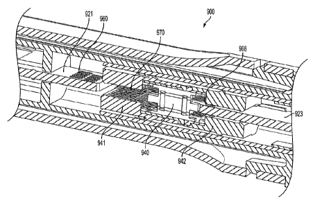
forty total conductive contacts are disposed along a top portion and obscured
from view.
[0068] Referring now to FIG. 9A, a cut-away side view of an electrical
connector 900
utilizing printed circuit boards during a mating process is shown. The
electrical connector
900 may be the same or similar to the electrical connector 100 of FIG. 1. A
mating end of a
plug assembly 904 is received by a mating end of a receptacle assembly 902.
Keying
elements or a latching system, as discussed in greater detail herein, may be
used to ensure the
plug assembly 904 and the receptacle assembly 902 are in the desired
orientation with respect
to each other before they are permitted to mate and fasten together. A plug
PCB 923
disposed within a cavity of the plug assembly 904 is electrically connected
with one or more
contact modules 940 having one or more conductive contacts. When mating of the
plug
assembly 904 and the receptacle assembly 902 is complete, one or more of the
conductive
contacts of the contact modules 940 will establish a conductive pathway
between the plug
PCB 923 and a receptacle PCB 921. Thus, a plug cable bundle 932 may be
electrically
connected with a receptacle cable bundle 930 via the electrical connector 900.
[0069] FIG. 9B shows a cut-away perspective view of the electrical
connector 900 of
FIG. 9A during the mating process. As shown, the plug PCB 923 is electrically
connected
with a plurality of conductive contacts 968 of the plurality of contact
modules 940. The
22
CA 02833265 2013-10-15
WO 2012/142606
PCT/US2012/033824
plurality of contact modules 940 are positioned and secured within the plug
assembly 904 of
the electrical connector 900 via a first contact module holder 941 and a
second contact
module holder 942. The receptacle PCB 921 includes a plurality of conductive
pads 960
disposed upon one or more surfaces of the receptacle PCB 921.
[0070] During the mating process, the receptacle PCB 921 is received
between upper and
lower portions of the first contact module holder 941 and the plurality of
conductive pads 960
are engaged by the plurality of conductive contacts 970 extending therefrom.
Staggering and
positioning of the plurality of contact pads 960 on a top and a bottom surface
of the
receptacle PCB 921 allows for a large number of electrical connections to be
made by the
electrical connector 900. In an alternative embodiment, the plurality of
contact pads 960 may
not be staggered or may be positioned on greater or fewer surfaces of the
receptacle PCB
921.
[0071] FIG. 10A shows a side view of a mated configuration for an
electrical connector
1000 utilizing printed circuit boards when the mating process has completed
while FIG. 10B
shows an enlarged view of the mated configuration for the electrical connector
1000 of FIG.
10A. The electrical connector 1000 may be the same or similar to the
electrical connector
900 of FIGS. 9A and 9B. As seen, a curved portion of a plurality of contacts
1070 have
engaged with a plurality of contact pads positioned on a top surface and a
bottom surface of a
PCB 1023 in order to establish an electrical connection therebetween.
[0072] Referring lastly to FIG. 11, a perspective view of a mating end of a
plug assembly
1100 of an electrical connector is shown to demonstrate its keying and
latching abilities. A
plug body 1108 contains keying protrusions or elements 1102 and 1104 for
ensuring the plug
body 1108 of the plug assembly 1100 is in the proper orientation with respect
to a
corresponding receptacle assembly for proper mating. The corresponding
receptacle
assembly may thus include keying slots (e.g., the keying slots 330 and 340
shown in FIG. 3)
23
CA 02833265 2013-10-15
WO 2012/142606
PCT/US2012/033824
for receiving or accepting the keying protrusions (1102, 1104). If the keying
protrusions
(1102, 1104) are not appropriately orientated with the keying slots of a
corresponding
receptacle assembly, the plug assembly and the corresponding receptacle
assembly will not
mate together.
[0073] Such keying can help reduce damage to a mated pair connector by
preventing
improper fastening of the mated pair connector together. In addition, keying
also helps
reduce risk of damage to electronics connected via the mated connector.
Although FIG. 11
shows two keying elements (1102, 1104) being used, in an alternative
embodiment, greater or
fewer keying elements may be utilized. Moreover, in an alternative embodiment,
keying may
be accomplished in a variety of manners (e.g., via a shape of the mating ends
of the plug and
receptacle assemblies themselves).
[0074] In addition, a latching mechanism 1106 is also coupled with the plug
body 1108
and operates to fasten or secure the plug assembly 1100 and a corresponding
receptacle
assembly together after mating has completed. Such latching can help ensure
the mated pair
connector does not unintentionally disconnect after the mating process has
completed. Once
the plug assembly 1100 is mated with the corresponding receptacle assembly,
the latching
mechanism 1106 on the plug body 1108 snaps or latches to a portion of the
corresponding
receptacle assembly. To disengage the plug assembly 1100 from the
corresponding
receptacle assembly, a disengagement button or element 1107 on the plug body
1108 can be
pressed or otherwise manipulated to unlatch the latching mechanism 1106 from
the portion of
the corresponding receptacle assembly. Alternative embodiments may utilize
other manners
of fastening and disengagement, for example, threaded components that screw
into place to
ensure the plug assembly and the corresponding receptacle assembly do not
decouple
unintentionally.
24
CA 02833265 2013-10-15
WO 2012/142606
PCT/US2012/033824
[0075] FIG. 12A shows an embodiment of a contact module 1200 for use in an
electrical
connector. Certain features of the contact module 1200 may be the same or
similar to the
contact module 500 previously described for FIG. 5. The contact module 1200,
however,
incorporates a plurality of wafers or platforms (1202, 1204, 1206, 1208) for
holding a
plurality of conductive contacts 1210. The contacts 1210 may be the same or
similar to the
conductive contacts (501, 502, 503, 504) previously described for FIG. 5.
Thus, rather than a
plurality of contact modules configured to slide within and engage in a
parallel configuration
with a module holder (see FIG. 5 and FIG. 6), the contact module 1200 is a
stable block or
stack securely fastening all of the contacts 1210 utilized in the electrical
connector in position
with one another. An electrical connector utilizing the contact module 1200
may be cheaper
to manufacture due to fewer mechanical parts, but may provide less flexibility
in
modification or customization. In certain embodiments, the contacts 1210 of
the contact
module 1200 may be removably inserted within openings of the contact module
1200 to
allow for increased modibility.
[0076] FIG. 12B shows the contact module 1200 of FIG. 12A, but in an
exploded
configuration. Thus, the first wafer 1202 is shown separated from the second
wafer 1204
which is shown separated from the third wafer 1206 which is shown separated
from the
fourth wafer 1208. A plurality of connecting protrusions 1220 and associated
connecting
holes 1230 are disposed on or within the four wafers (1202, 1204, 1206, 1208)
for coupling
the four wafers (1202, 1204, 1206, 1208) together to form a stable unit. The
connecting
protrusions 1220 may lock or press in place with the associated connecting
holes 1230 and be
held in place due to friction. In an alternative embodiment, additional, fewer
or other
fastening materials or manners may be utilized, for example adhesives, to
couple the four
wafers (1202, 1204, 1206, 1208) with one another.
CA 02833265 2013-10-15
WO 2012/142606
PCT/US2012/033824
[0077] FIG. 13 shows an embodiment of a plug assembly 1300 of an electrical
connector
utilizing a contact module 1340. The contact module 1340 may be the same or
similar to the
contact module 1200 previously described for FIGS. 12A-B. Moreover, certain
features of
the plug assembly 1300 may be the same or similar to the plug assembly 400
previously
described for FIG. 4. The plug assembly 1300 includes a plug body 1352, the
contact module
1340 configured to fit within the plug body 1352, and a wafer carrier or
contact module
holder 1302 for securing the contact module 1340 in position within the plug
body 1352. The
wafer carrier 1302 may be manufactured or formed as a single component, thus
providing for
less expensive manufacturing costs, but at a potential loss in modability when
compared to
the separate first module holder 414, second module holder 415 and PCB holding
member
410 previously described for FIG. 4. The plug assembly 1300 may also include a
plug
housing (not shown) that connects with the plug body 1352, the same or similar
to the plug
housing 411 previously described for FIG. 4.
[0078] As shown, the plug body 1352 has a mating end 1356 and a plurality
of slots or
contact pockets 1370 adjacent to the mating end 1356 for accepting a portion
of the contacts
1342 of the contact module 1340 when the contact module 1340 is secured within
the plug
body 1352. Similarly, a plurality of slots or contact pockets 1330 are
disposed near a mating
end 1306 of the wafer carrier 1302 for accepting a portion of the contacts
1342 of the contact
module 1340. A protective shroud 1312 extends beyond the plurality of slots or
contact
pockets 1330 of the wafer carrier 1302 in order to provide additional
protection or support for
the contact module 1340.
[0079] The plug body 1352 also incorporates a cutout 1360 for engaging with
a retention
member 1310 of the wafer carrier 1302 in order to securably hold the plug body
1352, the
contact module 1340 and the wafer carrier 1302 together as a stable unit. A
PCB end 1354 of
the plug body 1352 and a PCB end 1304 of the wafer carrier 1302 are configured
to receive
26
CA 02833265 2013-10-15
WO 2012/142606
PCT/US2012/033824
or accommodate a plug PCB (not shown) that slidably engages with a groove 1320
of the
wafer carrier 1302 for electrical connection with one or more wires or
conductive cables.
Electrical contact pads on the plug PCB engage with a portion of the contacts
1342 of the
contact module 1340, the same or similar as previously described for FIG. 4.
FIG. 14 shows
an enlarged cut-away perspective view of a plug assembly 1400 of an electrical
connector
utilizing a contact module 1440 disposed therein. The plug assembly 1400 may
be the same
or similar to the plug assembly 1300 previously described for FIG. 13.
[0080] As shown, a plug body 1452 having a mating end 1456 is engaged with
a wafer
carrier 1402 disposed therein and coupled with the contact module 1440 having
a plurality of
contacts 1442. The plurality of contacts 1442 are accepted by a plurality of
corresponding
slots or contact pockets 1470 in the plug body 1452 or a plurality of
corresponding slots or
contact pockets 1430 in the wafer carrier 1402, the same or similar as
previously described
for Fig. 13. The wafer carrier 1402 is engaged with the plug body 1452 via a
retention
member 1410 of the wafer carrier 1402 that snaps or otherwise engages with an
opening or
tab of the plug body 1452. A plug PCB (not shown) with conductive pads
disposed thereon
may thus be received within the wafer carrier 1402 and electrically connect
with the contacts
1442 (i.e. the contacts 1442 shown on the left-hand side of the contact module
1440).
Similarly, the contacts 1442 shown on the right-hand side of the contact
module 1440 are
configured to engage with and electrically connect with conductive pads of a
receptacle PCB
of receptacle assembly (not shown) when the plug assembly 1400 is mated with
the
receptacle assembly.
[0081] FIG. 15 shows an exploded perspective view of a plug assembly 1500
of an
electrical connector utilizing a contact module 1540 for connection with
printed circuit
boards. The plug assembly 1500 may be the same or similar to the plug assembly
1400 of
FIG. 14 or the plug assembly 1300 of FIG. 13. The plug assembly 1500 includes
a plug body
27
CA 02833265 2013-10-15
WO 2012/142606
PCT/US2012/033824
1552, a contact module 1540 configured to fit within the plug body 1552, and a
wafer carrier
1502 for securing the contact module 1540 in position within the plug body
1552. The plug
body 1552 has a PCB end 1554 for receiving at least part of the wafer carrier
1502 and a
mating end 1556 defining an opening 1580 providing access to one or more slots
or contact
pockets 1570, each slot or contact pocket 1570 configured to accept one of a
plurality of
contacts 1542 of the contact module 1540 when the contact module 1540 is
disposed within
the plug body 1552.
[0082] The contact module 1540 is coupled in place within the plug body
1552 via the
wafer carrier 1502 having a mating end 1505, a PCB end 1504 and a retention
member 1510
configured to engage with an opening 1560 of the plug body 1552, the same or
similar as
previously discussed. The plug body 1552 also includes a tab or attachment
component 1525
for mechanically fastening with a plug housing (not shown), the same or
similar as previously
described. The plug body 1552 also includes a latching mechanism 1506, the
same or similar
to the latching mechanism 1106, and disengagement button or element 1507, the
same or
similar to the disengagement button or element 1107. In addition, the plug
body 1552
includes a keying protrusion or element 1574 for ensuring the plug body 1552
of the plug
assembly 1500 is in a proper orientation with respect to a corresponding
receptacle assembly
during mating, the same or similar as previously described for the keying
protrusion 1104 of
FIG. 11. Additional keying protrusions (e.g., a keying protrusion 1572) may be
disposed on
other surfaces of the plug body 1552. In an alternative embodiment, other
methods of keying
or fastening a plug assembly to a receptacle assembly, the same or similar as
previously
discussed.
[0083J FIG. 16 shows a perspective view of a mating end 1656 of a plug
assembly 1600
of an electrical connector and illustrates a plurality of electrical contacts
configured to
electrical connect with one or more components of a corresponding a receptacle
assembly.
28
CA 02833265 2013-10-15
WO 2012/142606
PCT/US2012/033824
The plug assembly 1600 may be the same or similar to the plug assembly 1500
previously
described for FIG. 15. The plug assembly 1600 includes keying protrusions 1672
and 1673, a
disengagement button or element 1607 for releasing the plug assembly 1600 for
a mated
configuration with a corresponding receptacle assembly, an opening 1660 for
coupling with a
wafer carrier or module holder disposed within and an attachment component
1625 for
coupling with a plug housing, the same or similar as previously described. A
mating end
1656 is clearly seen having an opening 1680 for allowing a plurality of
electrical contacts
1642 received by a plurality of slots or contact pockets 1.670 formed via ribs
1672 to engage
with one or more conductive elements of a receptacle assembly when mated with
the plug
assembly 1600.
[0084] Although the embodiments previously described have shown various
connector
components as integrated or coupled to a plug assembly or a receptacle
assembly, the gender
of each assembly may be reversed or certain features of the plug assembly may
be
incorporated into the receptacle assembly and vice versa in an alternative
embodiment. An
alternative embodiment may also utilize greater or fewer connector components
than have
been described for the embodiments above. In one example, electrical contacts,
contact
modules, and/or contact module holders may be incorporated as part of a
receptacle
connector assembly and be configured to slidably mate with a printed circuit
board of a plug
assembly. In another example, only one of a plug assembly or a receptacle
assembly may
utilize a printed circuit board therein.
[0085] Exemplary embodiments of the invention have been disclosed in an
illustrative
style. Accordingly, the terminology employed throughout should be read in a
non-limiting
manner. Although minor modifications to the teachings herein will occur to
those well
versed in the art, it shall be understood that what is intended to be
circumscribed within the
scope of the patent warranted hereon are all such embodiments that reasonably
fall within the
29
CA 02833265 2013-10-15
WO 2012/142606
PCT/1JS2012/033824
scope of the advancement to the art hereby contributed, and that that scope
shall not be
restricted, except in light of the appended claims and their equivalents.