Note: Descriptions are shown in the official language in which they were submitted.
CA 2833344 2017-02-28
=
LIGHT EMITTING DIODE REPLACEMENT LAMP
[0001]
Technical Field
[0002] In various embodiments, the present invention relates generally to
illumination
systems and methods incorporating light emitting diodes (LEDs), and more
specifically to such
systems and methods that provide both direct illumination and decorative
illumination.
Background
[0003] Currently lighting applications are dominated by
incandescent lighting products.
Because they use hot filaments, these products produce considerable heat,
which is wasted, in
addition to visible light that is desired. Halogen-based lighting enables
filaments to operate at a
higher temperature without premature failure, but again considerable non-
visible infrared light
is emitted, and this heat is directed away from the lamp to the extent
feasible. This is
conventionally done by using a dichroic reflector shade that preferentially
passes the infrared as
well as a portion of the visible Light. The nature of this dichroic reflector
is such that it passes
several different visible colors as well as the infrared radiation, giving a
somewhat pleasing
appearance. This has led to numerous decorative applications for such halogen
lights. These
lights consume substantial current and dissipate considerable unwanted heat.
Halogen bulbs
are designed to operate at a variety of voltages between 12 volts (V) to as
high 15 V or greater.
[0004] Light emitting diodes have operating advantages compared to ordinary
incandescent
and halogen lights. LEDs typically emit a narrow range of wavelengths, thereby
eliminating, to
a large degree, wasted non-visible energy. White light can be created by
combining light
colors. LEDs can also emit in the ultraviolet wavelength range, in which case
white light (as
well as certain colors) can be created by excitation of a phosphor.
CA 02833344 2013-10-16
WO 2012/148585 PCT/US2012/028990
- 2 -
[0005] LEDs have an extremely long life compared to incandescent and
halogen bulbs.
Whereas incandescent and halogen bulbs may have a life expectancy of 2000
hours before the
filament fails, LEDs may last as long as 100,000 hours, and 5,000 hours is
fairly typical.
Moreover, unlike incandescent and halogen bulbs, LEDs are not shock-sensitive
and can
withstand large forces without failure, while the hot filament of an
incandescent or halogen
bulb is prone to rupture.
[0006] Halogen bulbs, incandescent bulbs, and LEDs all typically require
a fixed operating
voltage and current for optimal performance. Too high an operating voltage
causes premature
failure, while too low an operating voltage or current reduces light output.
Also, the color of
incandescent and halogen lights shifts toward the red end of the visible
spectrum as current and
voltage are reduced. This is in contrast to LEDs, in which only the intensity
of the light is
reduced. Furthermore, as the voltage to an incandescent or halogen light is
reduced, its
temperature drops; as a result, its internal resistance decreases, leading to
higher current
consumption but without commensurate light output. In cases where batteries
are used as the
source of energy, they can be drained without producing visible light.
[0007] Incandescent and halogen bulbs require a substantial volume of
space to contain the
vacuum required to prevent air from destroying the filament, to keep the glass
or silica
envelope from overheating, and to insulate nearby objects from the emitted
heat. In contrast,
LEDs, as solid-state devices, require much less space and generate much less
heat. If the
volume of an incandescent or halogen bulb is allocated to a solid-state LED
light, considerably
more functions may be incorporated into the lighting product.
[0008] Unlike incandescent and halogen lights, LEDs ordinarily produce
light in a narrow,
well-defined beam. While this is desirable for many applications, the broad-
area illumination
afforded by incandescent and halogen lights is also often preferred. This is
not easily
accomplished using LEDs. The light produced by incandescent and halogen lights
that is not
directed towards the target performs a useful function by providing ancillary
illumination and a
decorative function. Halogen lights with their dichroic reflectors do this
necessarily, but
ordinary incandescent lights can employ external shades, not part of the light
bulb, in a variety
of artistic designs to make use of this otherwise misdirected light.
SLTBSTITUTE SHEET (RULE 26)
CA 02833344 2016-04-14
- 3 -
Summary
[0008a] In accordance with an aspect of the present invention, there is
provided an
illumination device comprising: a housing; a power connector for connecting
the illumination
device to a power socket and receiving an input power; a first light emitter
disposed within the
housing; a first optical component for directing illumination generated by the
first light emitter
outside the housing in a first direction; a circuit for regulating the input
power and providing the
regulated power to the first light emitter; a second light emitter for
decorative illumination; and a
second optical component, separate from the first optical component, for
directing decorative
illumination therethrough outside the housing in a second direction, the
second direction being
different from the first direction.
[0008b1 In accordance with another aspect of the present invention, there
is provided a
method of using an illumination device to provide a decorative illumination
characteristic,
comprising: providing illumination from a first light emitter disposed within
a housing; directing
illumination generated by the first light emitter outside the housing in a
first direction using a
first optical component; providing decorative illumination, distinct from the
direct illumination,
from a second light emitter; and directing decorative illumination generated
by the second light
emitter through a second optical component outside the housing and in a second
direction,
wherein the second optical component is separate from the first optical
component and the
second direction is different from the first direction.
[0009] Embodiments of the present invention overcome the limitations of
halogen or
incandescent light sources, and combine their desirable properties with the
advantages afforded
by LEDs into a unique system. Various embodiments include systems and methods
that provide
direct illumination as well as decorative illumination distinct from the
direct illumination.
[0010] Embodiments of the present invention therefore include an LED-based
light
emitter (which includes one or more LEDs) for replacing standard incandescent
and halogen
bulbs for a wide variety of purposes. In accordance with various embodiments,
lighting systems
have enhanced functionality compared to that of conventional incandescent- or
halogen-based
lighting systems, and typically include a decorative illumination element that
provides, e.g.,
decorative illumination distinct from the direct illumination from the light
emitter.
CA 02833344 2016-04-14
- 3a -
100111 Some embodiments include an electrical connector or base the same
as or
equivalent to a standard bulb base, a printed circuit board (or other circuit
substrate or module)
electrically connected to the base, a driving circuit that may be mounted on
or embodied by the
printed circuit board, and/or one or more LEDs of one or more colors that may
be attached to the
printed circuit board. The driving circuit may include or consist essentially
of a solid-state circuit
that regulates the voltage and current available from the electrical source
(e.g., a power socket)
and regulates the output to a constant value utilized by the LEDs. The
available source voltage
may be either greater than or less than that utilized by the LEDs.
[0012] Various embodiments of the present invention include an LED lamp
that replaces
incandescent and/or halogen lamps as well as their decorative shades by
including LEDs on both
sides of the printed circuit (PC) board, where the decorative LEDs may be on
the opposite side of
that intended for direct illumination. The decorative LEDs may, for example,
illuminate an
envelope or shade around the lamp.
[0013] Lighting systems in accordance with various embodiments may also
include
additional circuitry, e.g., to allow remote control of lighting functions via
an infrared or wireless
device; to change the color of either or both of the (decorative) shade
illumination and the direct-
illumination LEDs; to impart a time-varying color and/or intensity to the
(decorative) shade
illumination and/or the direct illumination; to enable external switching via
mechanical action of
color, pattern, and/or intensity on either the shade or direct illumination;
and/or to
CA 02833344 2013-10-16
WO 2012/148585 PCT/US2012/028990
- 4 -
enable the switching of the various functions of color, intensity, and/or
pattern by interrupting
the power to the circuit within a predetermined time interval.
[0014] Mechanisms such as mechanical actuators that alter the pattern
and color of light to
the shade for the purpose of decorative illumination may also be included.
Such mechanisms
may be or include a shadow screen, a multi-faceted mirror, or other reflective
or diffractive
optical component or components either fixed within the envelope of the
lighting unit or which
are configured to move in order to vary the pattern and/or color of the
resulting light for
decorative and/or direct-illumination purposes.
[0015] Various embodiments of the present invention feature one or more
additional light
emitters such as LEDs disposed within the envelope (housing) of the light bulb
to provide the
decorative illumination. A separate, secondary circuit may be used to produce
a constant
current for the additional, decorative light emitter(s) and control their
decorative illumination
characteristics such as intensity, color, pattern, and/or frequency. The
secondary circuit may be
connected to the main source of power. Light generated from the decorative
light emitter(s)
may be guided along at least a portion of the length of an optical component
and exit the
housing through openings on the shade of the housing. Such embodiments may
include a
secondary optical element to direct light generated by the light emitter for
direct illumination
(e.g., the primary-illumination LED(s)) to provide the decorative
illumination. A heat sink may
be thermally connected to any or all of the light emitters for regulation of
their temperature. A
circuit may provide remote control of lighting functions of the lighting
system (e.g., the
decorative light emitter(s)) via, e.g., an infrared or wireless device.
[0016] One or more optical components may be disposed within the
housing, and may
direct a first, larger (e.g., more intense) portion of light generated by the
light emitter(s) for
direct illumination and direct a second, smaller (e.g., less intense) portion
of light for decorative
illumination. The second portion of light may be guided along the length of a
secondary
optical component and exit the housing through one or more openings on the
shade of the
housing. In an alternative embodiment, the decorative illumination is achieved
by light
emission through a plurality of light paths connecting the housing and the
optical component
that directs the second portion of light from the light emitter.
SUBSTITUTE SHEET (RULE 26)
CA 02833344 2013-10-16
WO 2012/148585 PCT/US2012/028990
- 5 -
Brief Description of the Drawings
[0017] In the drawings, like reference characters generally refer to the
same parts
throughout the different views. Also, the drawings are not necessarily to
scale, emphasis
instead generally being placed upon illustrating the principles of the
invention. In the
following description, various embodiments of the present invention are
described with
reference to the following drawing, in which:
FIG. 1 illustrates various views of an exemplary halogen illumination device
referred to
commonly as an MR-16.
FIG. 2 illustrates various view of an embodiment of the present invention that
can
retrofit the halogen illumination device and contains LEDs for illumination on
one side and
LEDs for direct illumination on the other. Circuitry to enable regulation and
other features is
also shown.
FIG. 3 illustrates various views of an embodiment of the present invention in
which
high intensity LEDs are placed on both sides to produce shade illumination and
direct
illumination. A switch and circuitry for changing the attributes of the
lighting is also shown.
FIG. 4 illustrates various views of another embodiment of the present
invention in
which a movable, multifaceted mirror is included on the shade side of the
illumination unit to
provide a variable pattern on the shade.
FIG. 5A illustrates various views of another embodiment of the present
invention in
which an internal fixture containing apertures is included to pattern
illumination to the shade.
FIG. 5B is a sectional view of another embodiment of the present invention in
which an
additional LED is disposed within the housing to produce decorative
illumination.
FIG. 5C is a sectional view of another embodiment of the present invention in
which
decorative illumination arises from an optical component that directs light
generated from the
primary light emitter.
FIG. 5D is a sectional view of another embodiment of the present invention in
which a
plurality of the light paths, connecting the housing and the optical
component, direct a portion
of the light from the primary light emitter for decorative illumination.
SUBSTITUTE SHEET (RULE 26)
CA 02833344 2013-10-16
WO 2012/148585
PCT/US2012/028990
- 6 -
FIG. 6 shows elevational and top views of a means for producing a
series/parallel
circuit comprised of individual LED semiconductor chips on a circuit board
that results in a
high-density lighting array.
FIG. 7 shows elevational and top views of an embodiment of the high-density
LED
array coupled with an integrated lens array that is movable to produce
variable-directional
lighting.
FIGS. 8(a) and 8(b) schematically illustrate a constant-current implementation
of a
compact dc/dc boost converter with a feature that enables current regulation
of LEDs based on
the thermal environment.
FIGS. 9(a) and 9(b) schematically illustrate a compact constant-current
buck/boost
circuit for current regulation based on the thermal environment in accordance
with various
embodiments of the invention.
Detailed Description
[0018] FIG.
1 illustrates an incandescent halogen-type bulb commonly available. The
features of this bulb derive from its operating characteristics: it operates
at high temperatures;
it requires an evacuated envelope separated from the hot filament; it emits
large quantities of
infrared radiation experienced by the user as heat; and it consumes large
quantities of electrical
power. Nonetheless, these devices are in common usage and fixtures and
appliances have been
constructed to accommodate the form, fit, and function of these bulbs. This
particular unit is a
model MR-16.
[0019] The
essential components of the bulb include a connector 101 that attaches to a
standard source of electrical power (e.g., a power socket) that has a mating
adapter; an
evacuated transparent capsule 102 containing the hot filament 105; an envelope
103 that acts as
a shade and filter to allow infrared radiation to pass, while reflecting a
portion of the desirable
visible light to the objects below; and a transparent front cover 104 that
allows the radiation to
pass, while protecting the evacuated capsule 102 from breakage.
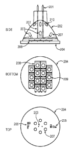
[0020] FIG. 2 illustrates an embodiment of the current invention. This
illuminating device
preferably has the same form, fit and function as the incandescent
illumination device of FIG. 1
and as such has a similar electrical connector 201 and similarly shaped
transparent or
translucent envelope 202. The envelope 202 will generally act to scatter light
emitted from
SUBSTITUTE SHEET (RULE 26)
CA 02833344 2013-10-16
WO 2012/148585 PCT/US2012/028990
- 7 -
inside the envelope and be visible from the outside. As such, the envelope 202
may serve as a
screen onto which are projected and displayed images, colors or other
decorative or
information-containing light either visible to humans or at shorter or longer
wavelengths. The
decorative or informational content may be generated by circuitry contained on
one or more
circuit boards 206 within the envelope of the bulb 202. This circuit 206 in
its simplest form
controls other illumination devices such as, e.g., the LEDs 207 located on the
back of the
circuit board 204. Another circuit 205 may be used to control high-power LEDs
209 in an
array 208 for direct illumination of objects outside the envelope of the
lighting device.
However, this circuit or circuits may enable several useful features,
including (i) a timer to
adjust the color and illumination level according to some preset or user-
adjustable schedule, (ii)
a photocell to turn the light on or off depending on the ambient light level
and or a proximity
sensor, (iii) a signaling function that communicates with other lights, and/or
(iv) a user-
accessible switch that enables switching of illumination characteristics such
intensity, color,
and/or continuous or flashing illumination modes.
[0021] Also typically located on circuit board 204 is a power-conditioning
circuit 205 that
regulates power to the high-intensity LEDs 208 located on the underside of the
board. This
circuit adapts and controls the power available via the connector 201 and
conducted to the
board via wires 203. The circuit 205 may contain storage features including a
battery to enable
the lighting device to act as an emergency light source in the event of a
power failure. The
circuit may rectify AC power to DC to suit the desired current and voltage
required by the
series and/or parallel array of LEDs and provide power to other on-board
circuitry.
[0022] In this embodiment, the LEDs 207 on the backside of the PC board
204 may serve
the function of communication and/or decoration. For decorative purposes, the
shade 202 is
preferably made of a colored or white transparent (or preferably translucent)
material such as
plastic or glass that is textured to scatter light. In this manner light from
the LEDs 207
impinges on this surface and is made more visible to the user, and may serve
the function of
decoration. The shade 202 may also contain penetrations 210 to allow heat to
exit the LED
enclosure.
[0023] FIG. 3 illustrates a similar incandescent replacement product.
This product also
contains an electrical connector 301, a shaped translucent or transparent
envelope 302 with
holes 310 to remove heat, one or more printed circuit boards 304 within the
enclosure, and
SUBSTITUTE SHEET (RULE 26)
CA 02833344 2013-10-16
WO 2012/148585 PCT/US2012/028990
- 8 -
means such as wires 303 to conduct electrical power to these board(s). This
embodiment has
high-intensity illumination LEDs 307 on the top surface and other high-
intensity LEDs 309 in
an array 308 on the bottom surface. Unlike the product of FIG. 2, which had
small LEDs with
a narrow exit beam and low intensity, these high intensity LEDs 309 and 307
have a higher
light output (generally greater than 10 lumens), and the exit angle of the
light may range from a
narrow angle to a very broad beam as desired. To control these LEDs,
additional circuitry may
be required as shown in the figure. In addition to the power-transforming
circuit 305 and the
control circuits 306, additional power handling circuits 311 may be included.
The high-power
LEDs may have one or more colored light outputs other than white, and have
different
orientations other than vertical to provide decorative illumination above the
lighting product. A
switch 311 that is accessible by the user may be used to control
characteristics of operation of
the lighting product.
100241 FIG. 4 illustrates another embodiment of the present invention.
Unlike the previous
examples in which modification of the color, intensity and pattern is
performed by electrically
controlling the electrical power to individual devices of one or more
orientations and/or color,
this embodiment contains a mechanical feature for varying the intensity and/or
pattern with
time. Variation is accomplished by, for example, a multi-faceted mirror 420,
operated by a
miniature electric motor 421 that changes the orientation and position of the
mirror. In this
way light is reflected or diffracted to form a pattern of shapes and/or color
on the translucent or
transparent envelope 402.
100251 FIG. 5A illustrates another embodiment that includes a patterned
mask 520 (or other
suitable means) that casts a shadow or other predetermined pattern by blocking
or otherwise
modifying the pattern of light emanating from the internal LEDs 507 located on
the back side
of the circuit board 504. Other features from other embodiments discussed
herein may also be
incorporated.
100261 FIG. 5B illustrates another embodiment in which an additional,
separate light
emitter 531 (such as, e.g., one or more LEDs) is controlled and/or powered by
a main
illumination circuit 532. The light emitter 531 may be coupled to separate and
dedicated optics
533 to provide flexibility in design, as light emitter 531 is generally meant
to provide
decorative illumination that is distinct from and that complements the direct
illumination from
the primary illumination source 534. For example, the decorative illumination
may be different
SUBSTITUTE SHEET (RULE 26)
CA 02833344 2013-10-16
WO 2012/148585 PCT/US2012/028990
- 9 -
from the direct illumination at least in terms of illumination direction,
color, and/or intensity.
Power is provided via connection of a power connector 535 to an input power
source, which,
for example, may be either 115 VAC or 12 VAC. A circuit 532 is preferably used
to convert
the alternating voltage to an approximately constant DC current.
[0027] Light generated by the primary illumination source 534 may be
directed by an
optical component 536 (e.g., a total-internal-reflection (TIR) optic) and exit
a substantially
transparent cover 537 attached to the housing (envelope) 538 to provide direct
illumination.
Electrical connector (or circuit) 539 typically connects the light emitter 531
to the circuit 532,
which may produce a smaller constant current for the decorative light emitter
531 than that for
the primary illumination source 534. Electrical connector 539 may be connected
to the main
power source; it may include or consist essentially of a resistor that limits
current to the
decorative light emitter 531 and that is in parallel to the primary
illumination source 534. The
circuit 539 may contain other suitable electronics that modulate or adjust the
decorative
illumination, such as the intensity, color, and/or frequency of the decorative
light emitter 531.
The light from the decorative light emitter 531 may be emitted in
substantially the same
direction as light from the primary illumination source 534, but separate
optics may be utilized
to accomplish the desired decorative illumination. For example, light-guiding
optics 533 may
include an optical light guide or a solid plastic pipe that directs light
along its length, creating a
linear "stripe" of light down the outside of the device.
[0028] A heat sink 540 may be thermally connected to the thermal path of
the illumination
device and thus regulate the temperature of the primary illumination source
534; the heat sink
540 may be co-linear with the light-guiding optics 533. Characteristics of the
decorative
illumination arising from light emitter 531, such as the intensity, color,
frequency, and/or
pattern of the light, may be responsive to a remote control that may be either
optical (e.g.,
infrared), wireless (e.g., radio-frequency), or wired (Ethernet, RS-232,
etc.).
100291 As described above, a backward-facing LED sharing a PCB with a
primary
illumination source may be used for decorative illumination. Furthermore, a
separate light
emitter, e.g., with dedicated control and/or power circuitry, in the housing
may provide
decorative illumination. In both cases, decorative illumination is formed
actively from a
secondary light emitter providing its own light.
SUBSTITUTE SHEET (RULE 26)
CA 02833344 2013-10-16
WO 2012/148585 PCT/US2012/028990
- 10 -
[0030] In another embodiment of the present invention, decorative
illumination is created
passively via utilization of a portion of the light from the primary
illumination source.
Reflecting optics may be used to direct light from light sources such as LEDs
for direct
illumination. Such reflecting optics may be aluminized reflectors that may
have a parabolic
shape to enhance the directionality of the forward light. The optics may also
include TIR
optics, which utilize the refractive index difference between two different
media to yield a
reflective internal surface. TIR optics are often very high efficiency (85-
90%) compared to
ordinary metal-coated reflectors. The design of both types of reflectors is
generally intended to
maximize optical efficiency with the goal of providing the highest degree of
illumination.
[0031] To provide illumination for decorative or other purposes not
involving direct
illumination, embodiments of the present invention use TIR and other
reflecting optics to divert
a portion of the light from its otherwise intended path by modifying the
optical design of the
TIR and other reflecting optics. A portion of light may be "siphoned off' in a
controlled way
and by means of reflection and refraction be redirected to create the
decorative or other non-
direct-illumination function. The redirected light may then be used to achieve
the desired
shape and color for decorative purposes.
[0032] FIG. 5C illustrates another embodiment of the present invention
in which a drive
circuit 551 converts the mains voltage into a constant current for a primary
illumination source
552 (e.g., one or more LEDs). An optic 553 (which may include or consist
essentially of, e.g.,
a TIR lens) may be used to direct light generated by the primary illumination
source 552. A
first portion of light generated by the primary illumination source 552 is
guided for direct
illumination, and a second portion of light is guided for decorative
illumination. The first
portion of the light is usually larger (i.e., more intense) than the second
portion of the light.
The first portion of the light generated by the primary illumination source
552 may be directed
by the optic 553 and exit a substantially transparent cover 554 attached to
the housing
(envelope) 555 to provide direct illumination. The housing 555 may include a
shade (which
may be substantially translucent) and one or more openings 556 in an optical
component 557
(e.g., an optical waveguide that may be completely or partially transparent)
through which light
may exit as decorative illumination. Other approaches such as diffusion and
filtering of the
light by the optical component 557 may be employed to further condition the
light to meet
specific decorative or secondary illumination purposes.
SUBSTITUTE SHEET (RULE 26)
CA 02833344 2013-10-16
WO 2012/148585 PCT/US2012/028990
- 11 -
[0033] FIG. 5D illustrates another embodiment of the invention operating
via similar
principles. One or more light channels 581 may connect a housing 582 to an
optical
component 583 and be utilized to produce decorative illumination therethrough.
The light
channels 581 may be, e.g., substantially empty passages through the housing,
or they may be
partially or substantially filled with an optical waveguide material. A
portion of the light
generated by a primary illumination source 584 (e.g., one or more LEDs) may be
directed
through the light channels 581 and exit the housing 582 through complementary
openings 585
on the shade of the housing 582.
[0034] It may be appreciated from these descriptions that the LEDs used
in these
embodiments, though small, occupy considerable space that limits the overall
light output of
the product. This is due, at least in part, to the need to provide electrical
connections to each of
the semiconductor light-emitting chips that are housed in large packages that
provide both
electrical connections and a facility for removing heat and enabling passage
of useful light.
The packages also often contain a lens or mirror for shaping and directing
this light. While
these packages allow some freedom of use, they also limit the density and
eliminate the ability
to integrate the functions of heat dissipation, light direction and electrical
connection. Many of
these functions may be accommodated within a printed circuit board of
appropriate design for a
group of devices at the same time and within the circuit as it is formed.
[0035] One way of improving the light density of the overall product is
to incorporate the
light-emitting dies onto a suitable patterned circuit board that contains the
external circuitry
needed to power and connect the LED devices without the use of a package. FIG.
6 illustrates
such an arrangement. This embodiment includes or consists essentially of a
printed circuit
board having at least a middle portion 601 that may be the usual fiberglass
core or one that
contains metals, ceramics or other materials to enhance thermal conductivity,
a top metal clad
layer 603, and a bottom cladding layer 602. It should be well understood that
these top and
bottom layers can easily be patterned by such processes as etching. A light-
emitting assembly
may be attached to the patterned surface of cladding 603 by cementing it with
a thermally and
electrically conducting compound, by welding it, or using any other suitable
attachment
technique. The cladding 603 then may act as a thermal or electrical conducting
pathway, or
both. The light-emitting assembly may include a metal base 604 to which is
bonded a
semiconductor light-emitting chip 605. This light-emitting chip 605 typically
contains a p-n
SUBSTITUTE SHEET (RULE 26)
CA 02833344 2013-10-16
WO 2012/148585 PCT/US2012/028990
- 12 -
junction that emits light and conducting top and bottom surface layers for
electrical and thermal
contact. A conducting wire or tab connects the top conducting member of the
junction to the
opposite conducting pad on the next assembly, thus building up a circuit that
is in series. Using
a different connection scheme, but the same general approach, a parallel
connection may be
assembled. By doing this, a relatively dense build-up of light-emitting chips
may be assembled
using the thermal and electrical transfer characteristics of the printed
circuit board.
Furthermore, heat sinking, cooling or other components may be attached to the
board,
improving performance, for example on the back side 602 of the printed circuit
board.
Although not shown, it should be understood that this connection method may be
extended in
the two dimensions of the plane of the board.
[0036] Such chips as illustrated in FIG. 6 will generally emit light in
all directions. Such a
distribution of light may not be desired for many lighting applications.
Therefore, a matching
array of lenses that is positioned over the light-emitting chips may be
utilized. This separation
of the top lens array from the LEDs allows the lens array to be positioned
independently, so
that the light directed by the lens may be moved and/or focused by moving the
lens array in
three dimensions. The movement may be controlled via, for example, stepper
motors or
piezoelectric-activated motion controllers whose support electronics are also
contained on the
printed circuit board. The array of lenses may be molded from a transparent
clear or colored
material with a variety of spherical or hemi-spherical shapes.
[0037] FIG. 7 illustrates such an arrangement. A PC board 701 containing
patterned metal
traces 703 has located on its surface light-emitting portions featuring
semiconductor light-
emitting devices 705 that arc mounted on bases 704. These areas arc bonded
together with
electrically conducting wires or strips to form a series/parallel circuit.
Positioned over the top
of these light-emitting regions is a lens array 710 into which has been formed
(by a method
such molding) a matching series of optical elements. Three such elements of
two different
shapes labeled 711 and 712 are shown. This lens array 710 is spaced apart from
the
semiconductor array and mounted to facilitate external manipulation in one or
more of three
dimensions as shown by the opposing pairs of arrows. Hence, by moving the lens
array 710,
the light emitted from the matching LED array may be directed and focused as
required, in
essence steering the light beam. This may be controlled by onboard
electronics, and via remote
control or such other means as required such as proximity sensors, timers and
the like.
SUBSTITUTE SHEET (RULE 26)
CA 02833344 2013-10-16
WO 2012/148585 PCT/US2012/028990
- 13 -
[0038] These lighting products generally require a source of AC or DC
current. Although
LEDs utilize direct current, it is possible to use the LEDs to rectify AC
power provided the
number of LEDs is chosen to match the AC voltage. It is well understood how to
transform
AC power to DC. The use of DC power as supplied by batteries, however, may
present some
problems because as the battery voltage declines under load, the current drawn
by the LEDs
rapidly declines, owing to the extremely non-linear current-voltage
characteristics of the
diodes. Since the light output of a LED is typically directly proportional to
current (at least in
some regimes), this means the light output rapidly declines. On the other
hand, if battery
voltage exceeds a predetermined level, heating of the semiconductor junction
of the LED is
excessive and may destroy the device. Moreover, excess heat in the LED
junction may cause a
condition called thermal runaway, in which the heat raises the current drawn
at a given voltage,
leading to further heating, which in turn leads to greater current draw and
quickly destroys the
device. This may be a particular problem with high-power LEDs and requires
careful thermal
management.
[0039] In order to help avoid this problem it may be useful to fix the
current through the
LEDs rather than the voltage. Using a battery as the source of current,
however, presents a
problem because of the differing voltage and current behavior of the battery
power source and
the LED load. Therefore, a circuit may be utilized to regulate and fix the
current independent
of the voltage supplied by the battery. In the case where the battery voltage
is less than the load
voltage required by the series and/or parallel LED circuit, a boost circuit as
shown in FIGS.
8(a) and 8(b) may be employed. In these circuits an integrated circuit device,
IC1 801, is used
to control the charging and discharging of an inductor Ll 803. This integrated
circuit may be
any of several that are available such as the Texas Instruments TPS61040.
After a charging
cycle, the IC switches the circuit so that the inductor Li 803 is permitted to
discharge through
the load, which in this case is the light-emitting diodes 805. The current is
controlled via a
feedback resistor R1 806. The value of the resistor is chosen to fix the
maximum current that is
permitted to flow through the load, which in this case, is one or more LEDs
(LED1, LED2)
indicated at 805. This manner of control occurs because the voltage drop
across R1 806 is
compared to an internally generated reference voltage at pin FB of IC1 801.
When the two
voltages are equal the current is considered fixed and will be held to that
predetermined value.
A diode D3 802 is used to ensure protection of the ICI 801 in case the battery
source (not
shown) is connected backwards. The diode 804 allows current flow through the
LEDs 805 in
SUBSTITUTE SHEET (RULE 26)
CA 02833344 2013-10-16
WO 2012/148585 PCT/US2012/028990
- 14 -
only the forward, or light-emitting direction. In embodiments of this
invention, such a circuit
may be enclosed within the envelope of the bulb.
100401 The circuit shown in FIG. 8(b) differs from that of FIG. 8(a) in
that the former
contains an easy and inexpensive means of protecting the LEDs from excessive
current flow
and the runaway that results from high temperatures. In this circuit a
resistor with a positive
resistance rate of change with temperature, R2 807 is placed in series with a
fixed resistor.
Resistor R2 is physically located on the circuit board so as to be in the
thermal pathway of heat
emanating from the LEDs 805. Therefore, when the temperature of the LEDs 805
increases,
the resistance of R2 807 also increases, and its resistance is added to that
of R1 806. Since the
voltage drop across these combined resistances appears on the feedback pin FB
of IC1 801, the
increased voltage is interpreted as a request for decreased current. Hence,
the natural tendency
of the LEDs 805 to draw more current, which would ordinarily lead to the
failure of the part, is
averted by introducing a self-limiting control function.
100411 This circuit has the advantage of being very efficient and
compact and having built
into it a temperature regulation that allows the resulting system to
automatically adapt to the
thermal environment in which it is placed. Because of these attributes, it
may, for example be
put into a miniature lamp base of the kind used for flashlights (e.g., a PR-
type flange base).
[0042] However, one possible limitation of the circuit is that it may
only boost voltage
from a lower value to a higher value required by the LED load. Therefore, in
situations where
only one LED is required, but a higher input voltage is all that is available,
the excess voltage
will generally appear across the LED even if one of the circuits in FIG. 8 are
used. This may
cause an excessive current to be drawn, leading to premature failure of the
LED and/or
premature draining of the battery. To solve this problem, embodiments of the
invention feature
a circuit that is preferably still compact enough to fit into a bulb or bulb
base, and that is
capable of either raising or lowering the output voltage above or below the
voltage of the
incoming battery or other DC supply in order to maintain the desired current
through the LED
load. The circuit will either boost the voltage if the input voltage is lower
than required by the
LED or reduce the voltage if it is higher than that required to sustain the
necessary constant
current through the LED. It is understood that references to an LED connote
one or more
LEDs in a series, parallel or series/parallel circuit. Furthermore, because of
the deleterious
effects of temperature, this circuit typically has the ability to regulate the
current through the
SUBSTITUTE SHEET (RULE 26)
CA 02833344 2013-10-16
WO 2012/148585 PCT/US2012/028990
- 15 -
LED depending on the ambient temperature. The ambient temperature may be
determined by
the environment as well as heat dissipated by the circuit and the LED.
[0043] Such a circuit is depicted in FIG. 9. This circuit utilizes a so-
called Cuk converter
that is ordinarily used as an inverting-switching voltage regulator. Such a
device inverts the
polarity of the source voltage and regulates the output voltage depending on
the values of a
resistor bridge. In the illustrated embodiment, the inverter circuit has been
altered so that it acts
to boost the voltage output or buck the voltage input in order to maintain a
constant current
through the load represented by one or more LEDs 905. The circuit incorporates
an integrated
circuit IC1 901 such as the National Semiconductor LM2611 Cuk Converter or
equivalent. In
this circuit, the internal transistor of ICI is closed during the first cycle
charging the inductor
Li 902 from the battery source indicated as Vbat. At the same time the
capacitor C2 904
charges inductor L2 903, while the output current to the LEDs 905 is supplied
by inductor L2
903. In the next cycle the IC1 901 changes state to permit the inductor Li 902
to charge
capacitor C2 904 and L2 903 to discharge through the LEDs 905. The control of
the charging
power and current through the load is performed by the resistor network
including or consisting
essentially of R2 906a and R3 907a. The overall value of these resistors
together with the
current passing through the LEDs 905 from ground, sets a voltage that appears
on the feedback
pin (FB) of IC1 901. Resistor 907a has a positive temperature coefficient so
that its resistance
increases with temperature.
[0044] The current may also be altered to accommodate thermal effects such
as heat
dissipation by the LEDs, heat produced by the IC1 or other circuit components
and/or the
ambient environmental conditions. This is effected by a temperature-dependent
resistor R3. In
FIG. 9(a), resistor R3 907a has a positive temperature coefficient in which
the resistance
increases with temperature. The additive effect of the series circuit with R2
906a means that as
temperature rises, the overall resistance of the combination does also,
leading to an increase in
voltage drop. This in turn causes IC1 to decrease the output current to the
LEDs 905. In FIG.
9(b) the resistor network includes resistors in parallel and series. In this
instance, resistors R2
and R4 906b, 908 are fixed and resistor R3 907b is temperature-dependent with
a positive
temperature coefficient. The use of a parallel arrangement allows a greater
freedom of choice
of temperature dependence than a simple series arrangement.
SUBSTITUTE SHEET (RULE 26)
CA 02833344 2013-10-16
WO 2012/148585 PCT/US2012/028990
- 16 -
[0045] The terms and expressions employed herein are used as terms and
expressions of
description and not of limitation, and there is no intention, in the use of
such terms and
expressions, of excluding any equivalents of the features shown and described
or portions
thereof In addition, having described certain embodiments of the invention, it
will be apparent
to those of ordinary skill in the art that other embodiments incorporating the
concepts disclosed
herein may be used without departing from the spirit and scope of the
invention. Accordingly,
the described embodiments are to be considered in all respects as only
illustrative and not
restrictive.
[0046] What is claimed is:
SUBSTITUTE SHEET (RULE 26)