Note: Descriptions are shown in the official language in which they were submitted.
VOLTAGE SAG CORRECTOR USING A VARIABLE DUTY CYCLE
BOOST CONVERTER
TECHNICAL FIELD
The present disclosure relates generally to providing voltages temporarily to
a
load during momentary electrical disturbances in the power supply line, and
more
particularly relates to an apparatus that compensates for voltage sags by
using a variable
duty cycle boost converter to boost the line voltage to predetermined desired
voltage
levels during occurrence of the voltage sags (a/k/a momentary electrical
disturbances),
thereby maintaining uptime and productivity across a connected load.
BACKGROUND
The five commonly observed power supply line disturbances are voltage surges,
voltage sags, overvoltage, under-voltage, and brownouts. Of these, voltage
sags
account for 90-95% of events, particularly in commercial and industrial
facilities.
Voltage sags are voltage reductions in the nominal line voltage. Typically,
voltage sags
are characterized by drops of between 10% - 90% of nominal (system) line
voltages.
The drops in voltage typically last from a cycle (16.6 millisecond) to a
second or so, or
tens of milliseconds to hundreds of milliseconds.
The reason for occurrence of voltage sags can be due to faults on the grid,
and
also due to high starting currents drawn by electrical loads (e.g., motors,
refrigerators,
freezers, air conditioners, etc.) at startup. Another reason for occurrence of
voltage sags
is faults in the power provider's transmission or distribution lines. Voltage
sags
CA 2833384 2019-01-21
CA 02833384 2013-10-16
WO 2012/145383 PCT/US2012/034050
occurring at high voltages typically spread through the electrical utility
network and are
transmitted to lower voltage systems via line transformers. Additionally,
voltage sags
can occur frequently in some locations that experience severe weather
phenomenon
such as lightning, wind, and ice. For example, lightning strikes a power line
and
.. continues to ground, which results in a line-to-ground fault. The line-to-
ground fault in
turn creates a voltage sag and this reduced voltage can be seen over a wide
area. The
amplitude of a voltage sag is the value of the instantaneous line voltage
during a voltage
sag. Generally, voltage sags are followed by a short duration increase (i.e.
inrush) in
the line current upon to nominal voltage levels due to discharge of reactive
impedance
in the load during the sag.
Power protection equipment to date has focused primarily on protecting
downstream (i.e. from the perspective of the power supply) electrical
equipment from
damage. Further, since typical power protectors are simple inexpensive
electrical
devices, having little or no power electronics for fast dynamic control, these
devices
have not been used to provide ride-through during an electrical line
disturbance.
Examples of typical power protectors include (but are not limited to) Metal
Oxide
Varistors (MOVs), relays, thermistors such as Negative Temperature Coefficient
(NTC) thermistors or Positive Temperature Coefficient (PTC) thermistors, etc.
For example, MOVs are used for protection against lightning strikes. NTC
thermistors or PTC thermistors are inserted for protection against inrush
current, and
relays are used to cut out equipment in case of damaging overvoltage events.
However, neither relays nor thermistors are able to provide ride through
functionality.
Ride through functionality involves providing temporary electrical energy to
synthesize normal operating conditions for a connected load or electrical
equipment,
during the occurrence of momentary electrical disturbances such as voltage
sags.
Such a functionality can be provided by a single device, or a combination of
electrical components connected in a certain arrangement. A ride-through
device
that is in common use is an uninterruptible power supply (UPS), or a voltage
sag
2
CA 02833384 2013-10-16
WO 2012/145383 PCT/US2012/034050
corrector, such as the dynamic sag corrector. However, these devices generally
do not
provide any protection functionality.
Therefore, it can be appreciated that what is needed is a device that protects
against common disturbances and also allows the machine/load/equipment to keep
operating through frequently occurring disturbances (e.g., voltage sags).
Voltage sags
are voltage reductions in the line voltage.
From various electrical power grid measurements, it has been determined that
voltage sags are statistically distributed in a manner such that a vast
majority of sags
retain at least 50% of the nominal line voltage value and last no more than 2-
3 seconds.
Conventionally, a typical sag correction device would involve the use of an
inverter to
inject the additional voltage needed, during the occurrence of a voltage sag,
with a normal
bypass arrangement to restore back to normal operating line conditions when
the sag is
over. However, such sag correction devices are typically very expensive.
Another possibility is to use an ac chopper arrangement to boost the incoming
line voltage to an appropriate value. Such a boost converter arrangement is
well
known to practicing engineers. However, boost converters suffer from a
significant
limitation in terms of speed of response - driven by a 'right half plane' zero
in the
control characteristics. Further, the need for gate drives and control logic
to
interconnect each element of the ac switches, adds to cost and 'real estate'
in a
product that is preferred to be compact and low-cost.
What is proposed in this disclosure is a low-cost arrangement of transient
voltage surge protection devices such as MOVs, relays for sustained
overvoltage and
under-voltage protection, and an arrangement of semiconductor devices such as
MOSFETs and diodes - along with their control, power supply and gate drive
circuits, that provide protection against the common disturbances, as well as
ride-
through for connected equipment, in the presence of frequently occurring power
disturbances - i.e. voltage sags. Thus, there is clearly a need for a combined
inexpensive
device that integrates protection and ride-through functions and does so
without
sacrificing the cost of the typical power protector.
3
CA 02833384 2013-10-16
WO 2012/145383 PCT/US2012/034050
BRIEF SUMMARY
Briefly described and according to one aspect, the present disclosure relates
to a
system for providing temporary electrical power to a load connected to an
input AC line
voltage during a voltage sag. The disclosed system includes a selectively
actuatable
boost converter for providing a boosted voltage to the load. Also provided is
a circuit
for detecting a voltage sag in the input AC line voltage corresponding to a
value in a
predetermined range of values in the input AC line voltage less than a nominal
voltage
for the input AC line voltage and for actuating the boost converter and for
detecting
when the voltage sag is over. Also included is at least one switch for
coupling the input
AC line voltage to the electrical load during normal operating conditions and
for
coupling the boost converter to the electrical load in response to detection
of a voltage
sag. Further, the system includes a clamping circuit coupled to the boost
converter for
clamping excess voltage from the boost converter when the boost converter is
turned off
in response to detection that the voltage sag is over.
According to another aspect, there is disclosed a method for providing
temporary electrical power to a load connected to an input AC line voltage
during a
voltage sag. Steps of the disclosed method include:
(1) detecting a voltage sag in the input AC line voltage corresponding to a
value
in a predetermined range of values in the input AC line voltage less than a
nominal
voltage for the input AC line voltage;
(2) actuating a selectively actuatable boost converter to provide a boosted
voltage to the load;
(3) detecting the end of the voltage sag; and
(4) in response to detection that the voltage sag is over, turning off the
boost
converter and clamping excess voltage from the boost converter to a clamping
circuit so
as to prevent the excess voltage from being transmitted to the load.
4
=
CA 2833384 2017-04-27
A further aspect of the present invention includes a system for providing
temporary electrical power to a load connected to an input AC line voltage
during a
voltage sag. The system includes a selectively variable voltage boost
converter
including a pulse-width modulated inductance for providing a boosted voltage
to the
load, the boost converter operative when actuated to provide a boosted voltage
as a
function of instantaneous value of the input AC line voltage compared to a
desired
nominal AC line voltage. A circuit is included for detecting a voltage sag in
the input
AC line voltage corresponding to a value in a predetermined range of values in
the input
AC line voltage less than the nominal voltage for the input AC line voltage
and for
actuating the boost converter to provide a boosted voltage at a value that
increases the
voltage provided to the load in response to detecting the voltage sag, for
detecting when
the voltage sag is over, and for deactuating the boost converter when the
voltage sag is
over. A switch is included for coupling the input AC line voltage to the
electrical load
during normal operating conditions and for coupling the boosted voltage from
the boost
converter to the electrical load in response to detection of a voltage sag and
actuation of
the boost converter. A clamping circuit is included and is coupled to the
boost converter
for clamping excess voltage from the inductance in the boost converter when
the boost
converter is deactuated in response to detection that the voltage sag is over.
A further aspect of the present invention includes a method for providing
temporary electrical power to a load connected to an input AC line voltage
during a
voltage sag. The method includes the steps of: (1) detecting a voltage sag in
the input
AC line voltage corresponding to a value in a predetermined range of values in
the input
AC line voltage less than a nominal voltage for the input AC line voltage, (2)
in
response to detecting the voltage sag, actuating a selectively variable
voltage boost
converter that includes a pulse-width modulated inductance to provide a
boosted voltage
to the load, the boost converter operative when actuated to provide a boosted
voltage as
a function of instantaneous value of the input AC line voltage compared to a
desired
nominal AC line voltage, (3) detecting the end of the voltage sag, and (4) in
response to
detecting that the voltage sag is over, deactuating the boost converter and
clamping
excess voltage from the inductance in the boost converter to a clamping
circuit so as to
prevent the excess voltage from being transmitted to the load.
4A
=
CA 2833384 2017-04-27
A further aspect of the present invention includes a system for providing
temporary electrical power to an electrical load connected to an input AC line
voltage
during a voltage sag. The system includes a selectively variable voltage boost
converter
including a pulse-width modulated inductor for providing a boosted voltage to
the
electrical load in response to actuation the boost converter operative when
actuated to
provide a boosted voltage as a function of instantaneous value of the input AC
line
voltage compared to a desired nominal AC line voltage. A clamping device is
included
and is coupled to the boost converter for absorbing excess voltage from the
inductance
in the boost converter upon turn off of the boost converter. A first voltage
sensor is
included for detecting the instantaneous value of the input AC line voltage. A
second
voltage sensor is included for detecting the instantaneous value of the
voltage at the
clamping device. A first switch (S1, S2) is included for coupling the input AC
line
voltage to the electrical load during normal conditions on the input AC line
voltage, for
disconnecting the input AC line voltage during charging of the boost
converter, and for
coupling the boost converter to the electrical load after charging. A third
switch (S3) is
included and is operative in alternation with the first switch for coupling
the boost
converter inductor through a low resistance to ground to charge the inductor.
A fourth
switch (S4) is included for coupling the clamping device through a discharge
resistor
(Re) in response to detection that the voltage on the clamping device has
exceeded a
predetermined threshold value. A control circuit is included for receiving
signals from
the first voltage sensor and the second voltage sensor, for detecting the
occurrence of a
voltage sag based on the signal from the first voltage sensor, for actuating
the boost
converter to provide the boosted voltage, for activating the first switch to
couple the
input AC line voltage to the electrical load during normal conditions on the
input AC
line voltage, for activating the third switch for charging the inductor in the
boost
converter, for detecting the end of the voltage sag based on the signal from
the first
voltage sensor, for deactuating the boost converter in response to detection
of the end of
the voltage sag, and for activating the fourth switch to discharge the
clamping device in
response to the signal from the second voltage sensor indicating that the
voltage on the
clamping device has exceeded the predetermined threshold value.
4B
CA 2833384 2017-04-27
A further aspect of the present invention includes a method for providing
temporary electrical power to an electrical load connected to an input AC line
voltage
during a voltage sag. The method includes the steps of (1) coupling the input
AC line
voltage to the electrical load during normal conditions on the input AC line
voltage, (2)
detecting the instantaneous value of the input AC line voltage, (3) in
response to
detection of a voltage sag, disconnecting the input AC line voltage from the
electrical
load, (4) subsequent to disconnection of the input AC line voltage from the
electrical
load after detection of the voltage sag, turning on a selectively variable
voltage boost
converter including a pulse-width modulated inductor to provide a boosted
voltage to
the electrical load, the boost converter operative when actuated to provide a
boosted
voltage as a function of instantaneous value of the input AC line voltage
compared to a
desired nominal AC line voltage, (5) coupling a boosted voltage from the boost
converter to the electrical load after charging of the boost converter, (6)
repeating the
steps of disconnecting the input AC line voltage, turning on the boost
converter, and
coupling the boosted voltage to the electrical load during the duration of the
voltage sag,
(7) in response to detection of the end of the voltage sag, disconnecting the
boost
converter from the electrical load to isolate the boost converter from the
electrical load,
(8) subsequent to disconnecting the boost converter from the electrical load,
turning off
the boost converter, (9) coupling a clamping device to the boost converter to
absorb
excess voltage from the inductor in the boost converter upon turn off of the
boost
converter, (10) in further response to the detection of the end of the voltage
sag,
reconnecting the input AC line voltage to the electrical load after excess
voltage from
the boost converter has been diverted to the clamping device, (11) detecting
the
instantaneous value of the voltage at the clamping device, and (12) in
response to
detection that the voltage on the clamping device has exceeded a predetermined
threshold value, discharging the clamping device through a discharge resistor
(Re).
4C
CA 02833384 2013-10-16
WO 2012/145383
PCT/US2012/034050
These and other aspects, features, and benefits of the claimed invention(s)
will
become apparent from the following detailed written description of the
preferred
embodiments and aspects taken in conjunction with the following drawings,
although
variations and modifications thereto may be effected without departing from
the spirit
and scope of the novel concepts of the disclosure.
BRIEF DESCRIPTION OF THE DRAWINGS
The accompanying drawings illustrate one or more non-limiting and non-
exhaustive embodiments of the present disclosure, and, together with the
written
description, serve to explain the principles of the disclosure. Wherever
possible, the
same reference numbers are used throughout the drawings to refer to the same
or like
elements of an embodiment, and wherein:
FIG. 1 shows a block diagram of a sag corrector circuit, according to one
embodiment of the present disclosure.
FIG. 2 (consisting of FIG. 2A, FIG. 2B, and FIG. 2C) shows exemplary output
voltage (appearing across the electrical load) waveforms, and timing diagrams
of
associated switches, when a sag occurs in the input AC line voltage.
FIG. 3 shows an exemplary sag corrector circuit, according to one embodiment
.. of the present disclosure.
FIG. 4 shows a state diagram representation of various switches used in
connection with the FIG. 3 embodiment.
FIG. 5 is a flowchart showing an exemplary microprocessor-implemented
process 500 corresponding to various steps executed in the microprocessor
logic as
followed in the embodiment shown in FIG. 3.
5
CA 02833384 2013-10-16
WO 2012/145383 PCT/US2012/034050
DETAILED DESCRIPTION OF DISCLOSED EMBODIMENTS
For the purpose of promoting an understanding of the principles of the present
disclosure, reference will now be made to the embodiments illustrated in the
drawings
and specific language will be used to describe the same. It will,
nevertheless, be
understood that no limitation of the scope of the disclosure is thereby
intended; any
alterations and further modifications of the described or illustrated
embodiments, and
any further applications of the principles of the disclosure as illustrated
therein are
contemplated as would normally occur to one skilled in the art to which the
disclosure
relates.
Aspects of the present disclosure relate to devices and methods that provide
voltages temporarily to a load during momentary electrical disturbances (e.g.,
voltage
sags) in the power supply line. According to one aspect, the disclosed device
is a sag
corrector circuit comprising a variable duty cycle boost converter circuit
that provides
the boost necessary to compensate for voltage sags. According to another
aspect, the
excess energy obtained via the boost converter is dumped to an energy clamp
circuit
coupled to the sag corrector circuit.
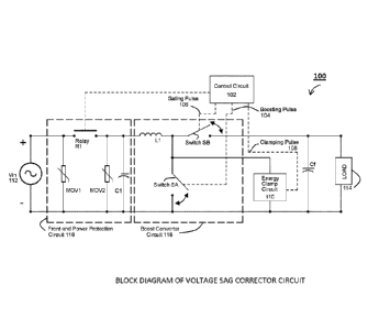
Referring now to the figures, FIG. 1 illustrates a block diagram of an
embodiment 100 of an exemplary sag corrector circuit. As shown, the disclosed
sag
corrector circuit connects the input AC line voltage (Vin) 112 to the load
114. In the
embodiment shown, the sag corrector circuit comprises a front end power
protection
circuit 116, a boost converter circuit 118, an energy clamp circuit 110, a
control circuit
102, and a filter capacitor Cf connected across the load.
Typically, the front end power protection circuit 116 includes non-linear
circuit
components such as varistors and other circuit components (e.g., relays etc.)
for
responding to power line disturbances such as over-voltages, sags, etc.
According to
one aspect, the front end power protection circuit 116 includes a MOV 1 with a
higher
6
CA 02833384 2013-10-16
WO 2012/145383 PCT/US2012/034050
voltage rating, a MOV2 with a lower voltage rating, and a relay R1 coupled
between the
two MOVs.
Coupled to the front end protection circuit 116 is a boost converter circuit
118
that comprises an inductor Li connected (in series to the input AC line
voltage) with a
switch SB, and another switch SA. The switch SA is oriented in a manner such
that one
terminal of the switch SA is connected to the inductor Li and the other
terminal is
connected in line with the neutral point of the input AC line voltage, e.g.
the switch SA
is connected in a parallel orientation to the load 114. The configuration for
the inductor
Li and switches SA and SB will be known to one skilled in the art on boost
converters.
Further, as will also be well known to people skilled in the art, the output
voltage of the boost converter (e.g., the load voltage) is controlled by
varying the
duty cycle of the switches SA and SB in a manner dependent on the
instantaneous value of the input AC line voltage and a pre-stored desired
(target) voltage. (Details of operation of switches SA and SB will be
discussed
later herein.) According to an aspect of the invention(s) as described herein,
the
varying of the duty cycle is effected using a pulse width modulation (PWM)
scheme,
at a predetermined boosting frequency.
In parallel arrangement with the front end power protection circuit 116 is a
capacitor Cl. As will be understood, the capacitor Cl (in conjunction with
other circuit
components of FIG. 1) enables the sag corrector to provide functionalities of
an
EMI/RFI filter.
An energy clamp circuit 110 is connected across the switch SA so that the
outcome of the boost converter operation of "boosting voltage levels" does not
cause the load voltage to exceed safe limits of operation. In other words, the
sag
corrector circuit 100 diverts current from the inductor Li into the energy
clamp circuit
110 to prevent load voltages from exceeding safe limits. In one embodiment,
the
energy clamp circuit 110 dissipates excess energy when actuated by clamping
pulses
108. The energy clamp circuit 110 shown in FIG. 1 is for illustrative
purposes. In one
example, the energy clamp circuit 110 involves a capacitor, a resistor,
diodes, and a
7
CA 02833384 2013-10-16
WO 2012/145383 PCT/US2012/034050
MOSFET switch. An alternate embodiment of the energy clamp circuit with a
reduced
component count (e.g., with lesser number of diodes than that will be required
for FIG.
1 embodiment) will be discussed exemplarily in connection with FIG. 3. As FIG.
1 is a
block diagram intended to provide a general overview of the functionality of
the
voltage sag corrector circuit 100, it does not show requisite components seen
in the
detailed diagram in FIG. 3 and other circuit components.
As shown in FIG. 1, the boost converter circuit 118 (whose output is connected
in parallel to capacitor Cf) is generally controlled by the control circuit
102 via gating
pulses 106 and boosting pulses 104. According to aspects of the present
disclosure, the
duty cycle of the boost converter 118 is regulated by varying the width of the
gating and
boosting pulses in a manner dependent on the instantaneous value of the input
AC line voltage and a pre-stored desired (target) voltage. With reference to
FIG.
1, the gating pulse 106 controls the operation of the switch SB, and the
boosting pulse
104 controls the operation of the switch SA. During a boosting phase, switch
SA is
turned on via boosting pulses 104, causing energy to be stored in the inductor
Li in the
form of magnetic flux. During a successive gating phase, the control circuit
102
provides gating pulses to the switch SA while the boosting pulse 104 is turned
off. As
will be understood, the sequence of operation of switches SA and SB is such
that the
inductor Li and the capacitor Cf charge and discharge alternately.
Specifically, while
the inductor Li is charging during a boosting phase, the capacitor Cf
(connected in
parallel to the load 114) is discharging through the load 114. Similarly, the
capacitor Cf
charges during a gating phase from the energy transferred by the inductor Li
to the
capacitor Cf. Exemplary waveforms showing a voltage sag as well as sequence of
operation of the gating pulse 106 and boosting pulse 104 will be discussed in
connection with FIG. 2A, FIG. 2B, and FIG. 2C. Specific examples
characterizing
particular circuit components that comprise the boost converter circuit 118
and the
energy clamp circuit 110 will be explained in connection with FIG. 3. Details
of
method steps implemented by the logic in the control circuit 102 will be
explained in
connection with FIG. 4.
8
CA 02833384 2013-10-16
WO 2012/145383 PCT/US2012/034050
As will be understood and appreciated, the inductor Li behaves like a short
circuit during normal operation of the sag corrector circuit, i.e. when no
voltage sags
occur. In one example (not shown herein), the control circuit 102 detects and
further
starts taking corrective action after about a quarter of an AC cycle following
the onset
of a voltage sag. According to aspects as described herein, the corrective
action
comprises the control circuit 102 turning off switch SB (e.g., turning off the
gating
pulse 106) and simultaneously turning on switch SA via boosting pulse 104. As
a
result, the load gets disconnected from the input AC line momentarily. During
a
successive time interval, the boosting pulse 104 is turned off while the
gating pulse 106
is turned on, and this process is performed repetitively, until the sag is
over. According
to aspects described herein, a predetermined delay is provided between
successive
gating and boosting pulses.
When the input AC line voltage returns to a nominal value at the end of a
voltage sag, rapid action is required to ensure that the load voltage does not
exceed
safe limits. This is accomplished by the control circuit 102 detecting a
return of the
AC line voltage to normalcy, and a rapid turn-off of switch SA and turn-on of
SB, with
a pre-determined delay between the turn-off and turn-on. During the
predetermined
delay (as mentioned above), current flowing through the inductor Li is
diverted into the
energy clamp circuit 110. Details of operation of the energy clamp circuit 110
will be
.. explained in connection with FIG. 2A, FIG. 2B, FIG. 2C, and FIG. 3. As will
be
understood, if no voltage sags are detected in the input AC line voltage, the
control
circuit 102 in the sag corrector circuit keeps monitoring the input AC line
voltage with
switch SB turned on and switch SA turned off.
Before proceeding further, it is noted herein that although the present
disclosure
discusses a sag corrector circuit connected to an electrical load, it will be
understood
that in alternate embodiments, the sag corrector circuit can be implemented in
different
circuit elements depending on the requirements of the connected load. For
example, a
sag corrector circuit can be integrated with electrical power supplies such as
switched
mode power supplies (SMPS) inside electronic devices, power protection strips
or surge
9
protectors, and various other circuit elements as will occur to those skilled
in the art.
For example, according to one aspect, the front end power protection circuit
can be
designed to handle various power line disturbances (e.g., voltage surges and
overvoltage
events) using a combination of circuit components and associated
microprocessor logic.
Details of systems and methods involved in voltage surges and overvoltage
events have
been disclosed in U.S. Patent No. 7,957,117 issued June 7, 2011, which may be
referred to
for further details. Exemplary output voltage waveforms and pulses (e.g.,
various
types of control signal) provided by the control circuit in an exemplary sag
corrector
circuit will be described next.
Now referring to FIG. 2 (consisting of FIGS. 2A, 2B, and 2C), exemplary output
voltage (appearing across the electrical load) waveforms 200A are shown,
during a
voltage sag and subsequent to recovery from a voltage sag. Referring first to
FIG. 2A, a
voltage sag 206 (Vg ) is shown as exemplified by a drop in the input AC line
voltage.
During the occurrence of a voltage sag, a corrected output voltage 204 appears
across
the electrical load as a consequence of corrective actions taken by an
embodiment of the
sag corrector circuit, wherein the sag corrector includes a variable duty
cycle boost
converter to take the corrective actions. The operation of the variable duty
cycle boost
converter involves the sag corrector alternately providing boosting and gating
pulses
non-concurrently, during the occurrence of a voltage sag. As mentioned
previously,
such boosting and gating pulses are usually provided by control circuit 102
included in
the sag corrector. Typically, and as shown, the gating pulses 106 and boosting
pulses
104 fluctuate rapidly at frequencies of about 16-25 KHz. Therefore, at the
time scale
resolution shown in the illustrations in FIG. 2A, details of individual pulses
are not
viewable. Such details are shown next in magnified views in FIG. 2B and FIG.
2C for
illustrating conditions during occurrence of a voltage sag and at the point of
recovery
from a voltage sag respectively.
Referring to FIG. 2B, a magnified view 200B of an exemplary corrected output
voltage 204 that appears across the electrical load is shown, during the
occurrence of a
voltage sag. The corrected output voltage 204 is the outcome of the boost
converter
CA 2833384 2017-08-16
CA 02833384 2013-10-16
WO 2012/145383 PCT/US2012/034050
operation and resembles an upwardly rising "step-like" waveform that closely
tracks the
waveform of a desired output voltage (Vdesired) 202. The desired output
voltage (Vdesired)
202 typically corresponds to a pre-stored desired template (e.g., a sequence
of samples
of a voltage profile) available to a control circuit (within the sag corrector
circuit).
In one aspect, the corrected output voltage 204 appears across a capacitor Cf
connected in parallel to the load (see FIG. 1 and FIG. 3). Further, as will
occur to one
skilled in the art, the corrected output voltage 204 appearing across the load
is the result
of corrective actions taken on the voltage sag 206 (Vsag ) by the control
circuit to
achieve the (target) desired output voltage (Vdesired) 202. As shown
exemplarily in FIG.
2B, the start of voltage sag correction occurs a time instant 205, and
continues until the
circuit recovers from the voltage sag at a subsequent time instant 214. As
will be
understood by one skilled in the art, the control circuit 102 (in the sag
corrector circuit)
has to detect a voltage sag first (e.g., by comparing instantaneous values of
the input AC
line voltage with samples of a pre-stored desired template voltage as
discussed in FIG.
5), and then start taking corrective action at time instant 205. In one
embodiment, the
voltage sag corrector detects a voltage sag at a time instant prior (e.g., at
a previous zero
crossing instant of the input AC line voltage) to time instant 205. The boost
converter
circuit 118 (shown in FIG. 1 and FIG. 3) is generally controlled by the
control circuit
102 via gating pulses 106 and boosting pulses 104.
According to aspects of the present disclosure, the duty cycle of the boost
converter 118 is calculated based on an instantaneous value of the input AC
line
voltage (e.g., a reduced value of the input AC line voltage as characterized
by
a voltage sag) and a desired (target) voltage, pre-stored within the memory of
the control circuit 102. In other words, the amount of "boost" needed depends
on the
instantaneous value of the input AC line voltage and a pre-stored desired
(target) voltage. Accordingly, the width of the gating and boosting pulses are
varied
(e.g., for how long they will be turned on) based on the calculated duty
cycle. After the
onset of a voltage sag and until the sag is over, the width (duration) of the
gating pulse
106 controls the operation of the switch SB, and the width (duration) of the
boosting
11
CA 02833384 2013-10-16
WO 2012/145383 PCT/US2012/034050
pulse 104 controls the operation of the switch SA. For example, as shown in
FIG. 2B,
boosting pulse 104a is of a narrower width than the boosting pulse 104b,
indicating the
different amounts of boost needed at the respective time instances of
providing boosting
pulse 104a and boosting pulse 104b. Although not specifically indicated in
FIG. 2B, it
will be understood that the width (duration) of the gating pulse 106 also
varies
accordingly, because of the complementary sequence of operation of the gating
and
boosting pulses. (A state diagram representation of the boosting and gating
phases is
shown in connection with FIG. 4.)
According to the laws of electromagnetic induction and during the occurrence
of
a voltage sag, alternate switching (of switches SA and SB via boosting and
gating
pulses respectively) causes the inductor Li (see FIG. 1 and FIG. 3) to charge
and
discharge repetitively. (In one aspect, and as discussed in FIG. 3, switch SA
comprises
a MOSFET switch and switch SB comprises a pair of MOSFET switches Si and S2.)
During a boosting phase, switch SA is turned on via a boosting pulse 104,
causing
energy to be stored in the inductor in the form of magnetic flux. During a
successive
gating phase, the control circuit 102 provides a gating pulse to the switch SA
while the
boosting pulse 104 is turned off. As a result, during the gating phase, thc
inductor
discharges by transferring the stored energy to charge a capacitor Cf (see
FIG. 1 and
FIG. 3) connected across the load. Thus, the capacitor Cf charges during a
gating phase
and discharges (through the load) during a boosting phase so as to regulate
(e.g.,
smoothen) the corrective voltage 204 appearing across the load during the
occurrence of
a voltage sag. In other words, the capacitor Cf charges during a gating phase
and
discharges during a boosting phase. Therefore, the inductor Li and the
capacitor Cf
charge and discharge alternately. Specifically, when the inductor Li is
charging during
a boosting phase, the capacitor Cf is discharging through the load. At a
successive
gating phase, the inductor discharges by transferring energy to the capacitor
Cf. This
charging/discharging of the inductor Li during the boosting/gating phases via
boosting/gating pulses results in the corrective voltage output (Vcorrected)
204 to appear
across the electrical load, as long as the voltage sag lasts. According to one
aspect,
12
CA 02833384 2013-10-16
WO 2012/145383 PCT/US2012/034050
during a voltage sag, the corrective voltage output 204 appearing across the
load can be
expressed as: Vcorrected = Vsag + (1-D)L1 di/dt, wherein during a voltage sag,
Vsag = V.,
D = duty cycle of the switch SB, and i = current flowing through the inductor
Ll.
However, it will occur to one skilled in the art that precision control of the
alternate turn on of the switches SA and SB (via boosting pulses 104 and
gating pulses
106 respectively) is difficult to achieve. Moreover, in the event that
switches SA and
SB are both turned on at the same time, the voltage across the load might
exceed safe
limits. Thus, according to one aspect of the present disclosure, a
predetermined delay is
provided between gating and boosting pulses. In one example and as shown in
FIG. 2B
and FIG. 2C, the delay is approximately 100 nanoseconds, although this delay
can vary.
During this delay, current flowing through the inductor Li is diverted into an
energy
clamp circuit 110.
The energy clamp circuit 110 (e.g., see FIG. 3) comprises a clamping
capacitor,
a diode, a MOSFET switch S4, and a resistor. Under normal operation, the
clamping
capacitor is charged to the peak of the line voltage, i.e. nominal voltage 210
as shown in
FIG. 2B. In one aspect, during the occurrence of a voltage sag, the clamping
capacitor
gets charged when switches SA and SB are turned off, for example, during the
predetermined delay between gating and boosting pulses. During this delay or
dead
time, the voltage (across the clamping capacitor) will typically rise above
the nominal
voltage, due to the current being diverted from the inductor Li, causing the
clamping
capacitor to get charged. Further, every time the sag corrector alternates
between gating
and boosting phases, the predetermined delay is provided, resulting in the
clamping
capacitor accumulating additional charge, as shown in FIG. 2B. Once the
voltage
across the clamping capacitor (a/k/a clamping capacitor voltage) reaches a
predetermined threshold, the energy clamp circuit 110 provides clamping pulses
108a
and 108b (e.g., to switch S4 in FIG. 3) to dissipate the energy stored in the
clamping
capacitor through resistor Re. The voltage across the clamping capacitor is
thus
maintained between a nominal voltage 210 and a predetermined threshold (e.g.,
predetermined threshold clamping voltage Va) 208 at all times. Therefore, the
energy
13
CA 02833384 2013-10-16
WO 2012/145383 PCT/US2012/034050
clamp circuit 110 (included in the sag corrector circuit 100) functions as an
"absorber"
for excess electrical energy that needs to be dumped, thereby preventing
voltages from
becoming too large and damaging the connected devices.
In one exemplary aspect, the control circuit 102 provides clamping pulses 108
to
the clamping capacitor after detection that the clamping capacitor voltage 212
has
exceeded a predetermined threshold, which can occur during a voltage sag, or
at the
point of recovery from a voltage sag. In one exemplary embodiment, such
clamping
pulses 108 are provided regardless of the state of the boost converter, i.e.
regardless of
whether the boost converter is in a boosting phase or a gating phase.
Now referring to FIG. 2C, a magnified view of the corrected output voltage 104
is shown zoomed in at the point of recovery from a voltage sag. For example,
it is
shown that at time instance 214, the control circuit determines that the
voltage sag is
over. At this instance, clamping pulse 108c is provided by the control circuit
to the
clamp circuit after detection that the clamping capacitor voltage 212 has
exceeded a
predetermined threshold clamping voltage (Va) 208. At time instant 214, switch
SB is
turned back on via the gating pulse 106 and SA is off (i.e. the boosting pulse
is off).
In the exemplary FIG. 2C, it will be observed that clamping pulse 108a (or
108b) is narrower than clamping pulse 108c implying that the energy stored in
the
clamping capacitor Cc at time instance 214 (i.e. at the point of recovery from
voltage
sag) is greater than a previous time instance in the middle of a voltage sag.
Consequently, it takes a longer time to discharge the clamping capacitor Cc.
This
phenomenon is likely possible at the point of recovery from voltage sags when
the
energy stored in the clamping capacitor is further elevated because of nominal
AC line
voltage levels (which are greater than voltage values during a voltage sag) is
added to
the "boost voltage" resulting from the inductor Ll.
It has been illustrated exemplarily in FIGS. 2B and 2C that three (3) clamping
pulses (e.g., 108, 108b, and 108c) are provided to the energy clamp circuit
110 during
the occurrence of a voltage sag, and another clamping pulse subsequent to
recovery
from a voltage sag. However, it will be understood that such illustrations are
for
14
CA 02833384 2013-10-16
WO 2012/145383 PCT/US2012/034050
purposes of example and explanation in this disclosure only. According to
aspects of
the present sag corrector, no limitation is imposed on the number of clamping
pulses,
particular instances at which they are provided by the control circuit, or
even the
duration of such clamping pulses. Details of an embodiment of the sag
corrector circuit
will be described in what follows next.
Now turning to FIG. 3, an embodiment 300 of a sag corrector circuit is shown.
As shown, the disclosed sag corrector circuit connects the AC line voltage
(Vin) 112 to
the load 114. In the embodiment shown, the sag corrector circuit comprises a
front end
power protection circuit 116, a boost converter circuit 118, an energy clamp
circuit 110,
a capacitor Cf connected across the load 114, and a control circuit 102 (for
controlling
the operation of the power protection circuit 116 and the boost converter
circuit 118 via
control signals or pulses).
Typically, the front end power protection circuit 116 includes non-linear
circuit
components such as varistors and other circuit components for responding to
power line
disturbances such as over-voltages, sags, etc. According to one aspect, the
front end
power protection circuit 116 includes a MOV1 with a higher voltage rating, a
MOV2
with a lower voltage rating, and a relay R1 coupled between the two MOVs. In
one
aspect, the relay R1 is actuated by a control signal (not shown in FIG. 3)
provided by a
control circuit 102 (e.g., at least one microprocessor along with associated
logic). The
front end power protection circuit also includes a voltage monitoring terminal
VM1 for
monitoring (e.g., continually measuring) the input AC line voltage for voltage
sags. In
one aspect, such measurement is performed periodically by a control circuit
102. In
parallel arrangement with the front end power protection circuit 116 is a
capacitor Cl.
As will be understood, the capacitor Cl (in conjunction with other circuit
components
of FIG. 3) enables the sag corrector to provide functionalities of an EMI/RFI
filter.
Coupled to the front end protection circuit 116 is a boost converter circuit
118
that comprises an inductor Li connected (in series to the input AC line
voltage) with an
AC switch SB, and another AC switch SA. In one example, the AC switch SA
comprises diodes Dl-D4 (connected in a full bridge rectifier mode) in parallel
CA 02833384 2013-10-16
WO 2012/145383 PCT/US2012/034050
arrangement with a MOSFET S3. The operation of the MOSFET S3 is controlled by
the
control circuit via boosting pulses 104. The switch SA is oriented in a manner
such that
one terminal (e.g., common to diodes D1 and D2) of the switch SA is connected
to the
inductor Li and the other terminal (e.g., common to diodes D3 and D4) is
connected in
line with the neutral point of the input AC line voltage.
As shown in FIG. 3, the AC switch SB comprises MOSFETS (a/k/a MOSFET
switches or simply, switches) Si and S2 connected in anti-parallel arrangement
with
diodes D7 and D8. In one exemplary embodiment, the diodes D7 and D8 may be
integrated with MOSFETS Si and S2. MOSFETS Si and S2 are controlled by the
.. control circuit, in particular by the gating pulses 106. Under normal
operating
conditions (e.g., when no sags occur), the switch SA (specifically, MOSFET
switch S3) is turned off (i.e., no boosting pulse 104 are provided), whereas
the
switch SB (specifically, MOSFET switches Si and S2) is turned on via gating
pulses 106, thereby allowing a direct connection between the AC line voltage
(Vin)
112 and the load 114.
It will be understood and appreciated that MOSFETS typically have high surge
current rating which makes them suitable for use in conditions when the load
is subjected to
high inrush currents, and obviates the requirement of bypass elements (e.g.,
thyristors)
that would otherwise be required to handle over-current stresses. For example
in FIG. 3,
at power-up, the output voltage is connected to the load (via switches Si and
S2) at
the zero crossing of the input AC line voltage, reducing the line inrush
current flowing
through the load.
Furthermore, connected in parallel to MOSFET switch S3 is an energy clamp
circuit 110. In one aspect, the energy clamp circuit 110 comprises a clamping
capacitor Cc, a diode D5, a MOSFET switch S4, and a resistor Re. According to
another aspect, the control circuit 102 provides a clamping pulse 108 to the
energy
clamp circuit 110 whenever the voltage (across the clamping capacitor Cc)
reaches a
predetermined threshold (e.g., threshold clamping voltage Va 208 shown in
FIGS.
2B and 2C). This methodology of providing an "absorber" for excess electrical
16
CA 02833384 2013-10-16
WO 2012/145383 PCT/US2012/034050
energy that needs to be dumped prevents voltages from becoming too large and
damaging the connected devices. In one exemplary aspect, the control circuit
102
monitors (e.g., measures) the voltage across the clamping capacitor Cc (also
referred to
herein as the clamping capacitor voltage 212) at a terminal called VM2 as
shown in
FIG. 3.
Under normal operation, the clamping capacitor Cc is charged to the peak of
the
line voltage. In one aspect, during the occurrence of a voltage sag, the
clamping
capacitor gets charged when switches SA and SB are turned off, for example,
during the
predetermined delay between gating and boosting pulses. Consequently, the
voltage
(across the clamping capacitor) will typically rise above the nominal voltage,
due to the
current being diverted from the inductor Li, causing the clamping capacitor to
get
charged above the nominal voltage. Further, every time the sag corrector
alternates
between gating and boosting phases, the predetermined delay is provided,
resulting in
the clamping capacitor accumulating additional charge above the nominal
voltage, as
shown in FIG. 2B. During such instances, and according to aspects described
herein,
the control circuit 102 provides a clamping pulse 108 to the energy clamp
circuit 110
(specifically, to the MOSFET switch S4). Once the voltage across the clamping
capacitor (a/k/a clamping capacitor voltage) reaches a predetermined
threshold, the
clamping pulse 108 provided to switch S4 causes the energy stored in the
clamping
capacitor to be dissipated through resistor Re. (See FIG. 2B for additional
details.)
Again, when the circuit recovers from a voltage sag (i.e. switch SA is turned
on
via gating pulse 106 and switch SB is turned off), the excess energy in the
inductor Li
is also diverted into the clamping capacitor in the energy clamp circuit 110.
As a result,
if the voltage across the clamping capacitor reaches a predetermined
threshold, another
clamping pulse 108 is provided to switch S4 so that the energy stored in the
clamping
capacitor is dissipated through resistor Rc. (See FIG. 2C for additional
details.)
As will occur to one skilled in the art, the diode D5 in the energy clamp
circuit
110 remains forward-biased relative to the electrical power supply such that
the initially
uncharged clamping capacitor Cc gets charged when the current flowing through
17
CA 02833384 2013-10-16
WO 2012/145383 PCT/US2012/034050
inductor Li (of the boost converter circuit 118) is diverted into the clamping
capacitor
Cc. But the diode D5 becomes reverse-biased once the clamping capacitor Cc
gets
charged, thereby preventing electrical charge stored in the clamping capacitor
Cc from
returning back to the AC line. Consequently, clamping pulses are provided by
the
control circuit 102 to the switch S4 so as to cause the capacitor to discharge
through
resistor Rc. Thus, the energy clamp circuit prevents a shoot-through of load
voltage,
during the occurrence of a voltage sag.
The resistor Re in the energy clamp circuit 110 does not see any dissipation
under normal conditions, but only when switch S4 is turned on as the result of
the
clamping capacitor voltage measured at VM2 being too high. Hence, the power
dissipation rating of Re can be relatively small. The clamping capacitor Cc
also helps
to limit the peak surge voltage that can be applied to the load. Thus, as will
be
understood, the diode D5 and the clamping capacitor Cc not only ensure that
the output
voltage does not exceed a desired value, but also ensures that current from
the inductor
Li is diverted into the energy clamp circuit 110 when switches Si/S2 and S3
are
transitioning. The voltage across the clamping capacitor Cc is regulated to a
value
marginally higher than the peak of the output voltage delivered to the load.
In one exemplary embodiment, the voltage across the clamping capacitor (a/k/a
clamping capacitor voltage 212) is constrained to lie between nominal voltage
210 and
a predetermined threshold clamping voltage (Va) 208 (see FIG. 2B and FIG. 2C
for
illustrative details). As a non-limiting example, for a capacitor Cc having a
rating of
300V that is operating on a nominal RMS line voltage of 120V, (or
equivalently,
nominal peak line voltage = 170V), the peak threshold clamping voltage Va =
210V. In
other words, the clamping capacitor voltage is allowed to fluctuate by 40V
above its
nominal peak value. The choice of the clamping capacitor Cc, thus arbitrarily
depends
on an allowable range of "safe" operation that is pre-decided by the circuit
designer.
Still referring to FIG. 3, a capacitor Cf is connected parallel to the load
114 so
as to regulate the corrected voltage appearing across the load, during the
occurrence of a
voltage sag. As mentioned previously, according to aspects of the sag
corrector circuit
18
CA 02833384 2013-10-16
WO 2012/145383 PCT/US2012/034050
300, during the occurrence of a voltage sag, the inductor Li (in the boost
converter
118) discharges by transferring its stored energy to charge the capacitor Cf.
In turn, the
capacitor Cf discharges through the load 114. In other words, the capacitor Cf
charges
during a gating phase and discharges during a boosting phase. A state diagram
representation of the boosting and gating phases is shown in connection with
FIG. 4.
As shown in FIG. 3, the boost converter circuit 118 (connected in parallel to
capacitor Cf) is generally controlled by the control circuit 102 via gating
pulses 106 and
boosting pulses 104. In particular, the gating pulse 106 controls the
operation of
switches Si and S2, and the boosting pulse 104 controls the operation of the
switch S3.
Under normal operating conditions, the gating pulse 106 is turned on and the
boosting
pulses 104 is turned off. After a voltage sag is detected, the boost converter
118 is
activated by alternately switching between gating and boosting phases. During
a
boosting phase, switch S3 is turned on via boosting pulse 104, causing energy
to be
stored in the inductor Li in the form of magnetic flux. During a successive
gating
phase, the control circuit 102 provides gating pulses to the switches Si and
S2 while the
boosting pulse 104 is turned off. As will be understood, the sequence of
operation of
switches Si, S2 along with switch S3 is in such a manner that the inductor Li
and the
capacitor Cf charge and discharge alternately. Specifically, while the
inductor Li is
charging during a boosting phase, the capacitor Cf (connected in parallel to
the load
114) is discharging through the load 114. Similarly, the capacitor charges
during a
gating phase from the energy transferred by the inductor Li to the capacitor
Cf.
Exemplary waveforms showing sequence of operation of the gating pulse 106
and boosting pulse 104 have been discussed in connection with FIG. 2A, FIG.
2B, and
FIG. 2C. According to an aspect of the invention(s), the frequency of
operation of the
switches Si, S2 and the switch (S3) for boosting and coupling the boosted
voltage to the
electrical load is in the range of about 16 kHz to about 25 kHz, although
other
frequencies of operation may be selected depending on other operational
parameters, as
will be understood by those skilled in the art.
19
CA 02833384 2013-10-16
WO 2012/145383 PCT/US2012/034050
To ensure safe switching, a predetermined dead-time of typically around 100
nanoseconds is needed between turn-off of a switch and turn-on of an incoming
switch, e.g., between successive boosting and gating pulses (see FIG. 2B and
FIG. 2C)
during a voltage sag. This reduces the possibility of a shoot-through or
instability at
the load, to reduce system losses, and to prolong the life of the switches.
The actual
duty cycle required is calculated by the control circuit 102 (e.g., a
microprocessor
therein) which looks at the input line voltage, compares this to a
predetermined
template desired output voltage, and calculates the duty cycle needed, and
regulates
the quantities via a control loop. In one embodiment, the sag corrector is
typically
designed only for short duration voltage sags, typically lasting for no more
than 2-3
seconds.
As will be understood, if no voltage sags are detected in the input AC line
voltage, the control circuit 102 in the sag corrector circuit keeps monitoring
the input
AC line voltage (e.g., at terminal VM1) with switches Si, S2 turned on, and
switches
53, S4 turned off.
As will be understood, input AC line voltages are rated at 120 V, 240 V, or
other
voltages in conjunction with an associated current that depends on the current
drawn by
a particular type of connected load. As will be known by those skilled in the
art, AC
line power voltages depend on national standards that differ from one country
to
another, or even from one electronic device to another. It will be understood
that
embodiments of the present disclosure are applicable universally to all kinds
of input
AC line voltages, and not necessarily limited to 120V RMS (i.e., 170V peak),
as
discussed herein. Alternate embodiments of the disclosed sag corrector circuit
can be
designed as will be apparent to one skilled in the art. For example, although
it is shown
in FIG. 3 that the control circuit monitors the voltages at terminals VM1 and
VM2 in
the sag corrector circuit, in alternate embodiments, there can be other
terminals (e.g.,
voltage appearing at the load) at which the control circuit can additionally
monitor
voltages / currents, as will occur to one skilled in the art.
CA 02833384 2013-10-16
WO 2012/145383 PCT/US2012/034050
Additionally, although not shown in FIG. 3, one or more power supplies may be
involved in the operation of the control circuit 102. Further, although not
shown in
FIG. 3, one or more microprocessors or microcontrollers or any other type of
state
machine in combination with each other may be involved in the operation of the
control
circuit 102. A state diagram representing sequence of operation of various
switches (via
pulses provided by the control circuit 102) in the sag corrector embodiment
shown in
FIG. 3, will be described next.
With reference to FIG. 4, shown is a state diagram 400 that shows the
sequence of operation of switches Sl/S2 and S3 that relates to the steps of
microprocessor logic executed within the control circuit 102.
The state diagram 400 includes a normal operating conditions state 404, a
gating phase state 408, a boosting phase state 406, and a clamping phase state
410.
After startup and assuming steady state has been reached, the control circuit
102
enters the normal operating conditions state 404. During this state, the
capacitor Cf
and the clamping capacitor Cc is fully charged to the peak of the input AC
line
voltage. As will be understood by one skilled in the art, the normal operating
conditions state 404 represents a nominal state of the sag corrector circuit,
when no
overvoltages/voltage sags/transients occur, or after recovery from a voltage
sag. If
electrical power is lost while the control circuit is in any other state, the
circuit
reverts back to the normal operating conditions state 404. Also, during normal
operating conditions state 404, the gating pulse 106 is provided to switches
Si and
S2, to connect the load to the input AC line voltage.
Upon occurrence of a voltage sag, the state of the control circuit changes
from
the normal operating conditions state 404 to a boosting phase state 406.
During the
boosting phase state 406, the control circuit 102 provides boosting pulses 104
to
MOSFET switch S3 while the switches Si and S2 are turned off. This results in
the
load being disconnected from the input AC line voltage. Also, turning on of
MOSFET
switch S3 results in energy getting stored in the inductor Li in the form of
magnetic
flux. During the boosting phase, the charged capacitor Cf discharges through
the
21
CA 02833384 2013-10-16
WO 2012/145383 PCT/US2012/034050
electrical load. As will be understood, the amount of "boost" needed in the
boosting
phase state 408 depends on the instantaneous value of the input AC line
voltage
and a pre-stored desired (target) voltage. Hence the duration of time for
which the
MOSFET switch S3 is turned on (a/k/a duty cycle of switch S3) depends on the
.. instantaneous value of the input AC line voltage (e.g., a reduced value of
the
input AC line voltage as characterized by a voltage sag) and samples of a pre-
stored desired (target) voltage.
As shown in FIG. 4, from the boosting phase state 406, the control circuit
enters a gating phase state 408 during which the control circuit 102 provides
the gating
pulses 106 and the boosting pulses 104 are turned off. Hence, during the
gating phase,
the control circuit 102 provides a gating pulse 106 to MOSFET switches Si and
S2
while the switch S3 is turned off. During the gating phase, the inductor Li
discharges
by transferring the stored energy to charge a capacitor Cf (see FIG. 1 and
FIG. 3)
connected across the load so as to regulate the corrected voltage 204
appearing across
the load during the occurrence of a voltage sag. As will occur to one skilled
in the art,
the capacitor Cf and the inductor Li follow a reverse order for
charging/discharging.
According to aspects of the present disclosure, the boosting phase and the
gating
phase occur non-concurrently, alternately switching between the gating phase
state 408
and the boosting phase state 406. Accordingly, after the onset of a voltage
sag and until
the sag is over, the width (duration) of the gating pulse 106 controls the
operation of the
switches Si and S2 in the gating phase state 408, and the width (duration) of
the
boosting pulse 104 controls the operation of the switch S3 in the gating phase
state 406.
However, it will occur to one skilled in the art that precision control of the
alternate turning on of the switches between the boosting phase state 406 and
the
.. gating phase state 408 (via boosting pulses 104 and gating pulses 106
respectively) is
difficult to achieve. Thus, according to one aspect of the present disclosure,
a
predetermined delay (i.e. dead time) is provided between the gating and
boosting phases
to ensure safe switching. During the delay, current flowing through the
inductor Li is
diverted into the energy clamp circuit 110, particularly to the clamp
capacitor Cc. Thus,
22
CA 02833384 2013-10-16
WO 2012/145383 PCT/US2012/034050
the clamping capacitor Cc accumulates charge every time the circuit alternates
between
gating and boosting phases, or vice-versa.
It will also occur to one skilled in the art that the clamping capacitor's
charge
cannot increase in an unbounded manner, i.e. the voltage across the capacitor
should be
controlled to a value less than a predetermined threshold less than the
voltage rating of
the capacitor. Therefore, in one embodiment, a clamping phase state 410 is
provided,
during which switch S4 is turned on via clamping pulses, regardless of the
condition of
the switches Si, S2, and S3. In other words, it will be understood that the
clamping
phase state 410 can be independent (e.g., unrelated to gating and boosting
phases), as
shown in FIG. 4. During the clamping phase state 410, the control circuit 102
provides
a clamping pulse 108 to the energy clamp circuit 110 (specifically to switch
S4)
whenever the voltage (across the clamping capacitor Cc) exceeds a
predetermined
threshold Va. As will be understood, the clamping pulse is provided to switch
S4 so
that the clamping capacitor Cc discharges through the resistor Rc. In one
exemplary
embodiment, the clamping capacitor discharges through the resistor Rc until
the
residual voltage in the clamping capacitor Cc reaches nominal voltage levels.
(e.g., see
FIG. 2B and FIG. 2C). (It will be recalled that under normal operation, the
clamping
capacitor Cc is charged to the peak of the line voltage, e.g., nominal voltage
levels.)
In one exemplary aspect, the control circuit monitors the voltage across the
clamping capacitor, e.g., as shown in FIG. 3. It will be understood that the
sag
corrector enters a clamping phase state whenever the voltage across the
clamping
capacitor Cc exceeds a predetermined threshold. In other words, it is possible
that the
clamping capacitor Cc exceeds a predetermined threshold during occurrence of a
voltage sag, and also during a subsequent instance of recovery from a voltage
sag.
During such instances, and according to aspects described herein, the control
circuit 102
provides a clamping pulse 108 to the energy clamp circuit 110 (specifically,
to the
MOSFET switch S4). (See FIG. 2B and FIG. 2C for illustrative examples of
clamping
pulses provided to switch S4 during a voltage sag, and another clamping pulse
to switch
S4 subsequent to recovery from a voltage sag.) From the clamping phase state
410, the
23
CA 02833384 2013-10-16
WO 2012/145383 PCT/US2012/034050
sag corrector circuit enters a non-clamping phase state 412, during which the
clamping
pulses are turned off.
In one aspect, the control circuit keeps monitoring the input AC line voltage,
e.g., at VM1 terminal in FIG. 3. In the event that the control circuit detects
that the
voltage sag has ended (voltage sag recovery), the sag corrector enters a
normal
operating conditions state 404, and normal conditions are restored (i.e.
switches Si,
S2 are on, switches S3, S4 are off). However, if the voltage sag has not
ended, then
after a predetermined delay (during which current from the inductor Li is
diverted
into the clamping capacitor), the circuit enters a boosting phase state 406.
As
mentioned previously, the sag corrector alternates between a gating phase
state 408
and a boosting phase state 406 with a predetermined delay in between the
states. In
one aspect, it will be understood that the normal operating conditions state
404 and
the gating phase state 408 have similar configuration of switches, e.g., S1=
ON, S2 =
ON, S3 = OFF, S4 = OFF. This usually happens at the point of recovery from a
voltage
sag. However, if a voltage sag is not over, then from the gating phase state
408, the
control circuit enters a boosting phase state 406, as explained previously.
Details of
the control circuit logic will be explained in what follows next.
Now turning to FIG. 5, an exemplary microprocessor logic 500 is shown as
steps of a flowchart, corresponding to the embodiment of the circuit 300
described
earlier in FIG. 3. Particularly, it will be understood that the steps shown in
FIG. 5 are
included as a program included in a microprocessor or microcontroller
contained in the
control circuit 102. As used herein, the terms "microprocessor" and
"microcontroller"
are used interchangeably, it being understood that many different types of
programmable microprocessors or microcontrollers may be utilized, provided
that such
devices can receive inputs representing the voltages measured as described
herein for
purposes of detecting a voltage sag or other power anomalies, and can provide
outputs
for controlling operation of the various switches and relays described herein.
In
particular, a microprocessor capable of determining the variable duty cycle
for the boost
converter is preferred. Further, a microprocessor capable of controlling the
actuation
24
CA 02833384 2013-10-16
WO 2012/145383 PCT/US2012/034050
and turnoff of the boost converter independently of control of the discharge
of the
clamping capacitor is preferred.
For the embodiment in FIG. 3, it is assumed that the Relay R1 is in the closed
position. It will be additionally understood that in one embodiment, various
method
steps in the control logic can occur unrelated (e.g., concurrently) with
various other
method steps. For example, as shown in FIG. 5, steps 522, 524, 526, and 528
occur
independently of steps 504, 506, 508, 510, 512, 514, 516, 518, and 520.
Further details
will be better understood from the description that follows.
As shown in FIG. 5, starting at step 502, the microprocessor powers on, or is
reset from a prior shutdown mode. The initial conditions for the switches are:
Sl= ON,
S2 = ON, S3 = OFF, S4 = OFF. This switch configuration allows the input AC
signal
to pass through Relay R1 and Inductor Li, and across capacitor Cf, thereby
charging the
capacitor Cf to the nominal line voltage (e.g., 120V AC). Although the relay
R1 is
primarily used for protection against over voltages and various other power
disturbances, the microprocessor logic 500 discussed herein does not
explicitly specify
protection against over voltages and various other power disturbances. Also,
in addition
to providing functionalitics as described in the boost converter, the inductor
Li, and
capacitors Cl and Cf also operate as an EMI/RF1 filter.
As mentioned previously, the switch configuration Sl= ON, S2 = ON, S3 =
OFF, S4 = OFF is equivalent to the gating pulse 106 being turned on (by the
control
circuit 102), and the boosting pulse 104 being turned off. Also, under normal
operating
conditions, the clamp capacitor Cc (in clamp circuit 110) is charged to the
nominal line
voltage.
At step 504, the input AC line voltage at point VM1 is sampled with circuitry
residing in the control circuit 102. Specifically, the microprocessor or some
external
circuitry is presented with a scaled down representation of the actual input
AC line
voltage as scaled by a voltage divider network or transformer. This scaled
down
voltage can be considered as a "representative AC voltage". For example, if
the
nominal input AC line voltage is 120V, for the microprocessor, an equivalent
voltage
CA 02833384 2013-10-16
WO 2012/145383 PCT/US2012/034050
scaled down voltage is for example 2V. Because of the one-to-one mapping
between
the "representative AC voltage" and the actual "input AC line voltage VM1
(a/k/a line
voltage at VM1)", the above-mentioned voltages have been used herein
synonymously.
In one example, the microprocessor or other circuitry samples the input
voltage VM1 at
a specific sampling frequency (S) to generate a set of samples VM1= (
VM1[1],VM1[2], VM1[3]...VMl[n]).
Then, the microprocessor determines (at step 506) whether or not VM1 matches
a template set of pre-stored sample values Vdesired ¨ (Vdesired [I], Vdesired
[2], Vdesiredd [3],
...Vdesired [n],..) on a sample-by-sample basis. For example, the pre-stored
template can
.. be derived by sampling a representative target (i.e. a non-voltage sag) AC
voltage
starting at a zero crossing at the same sampling frequency (S). As will be
understood,
under normal operating conditions, the representative input voltage VMl[n]
would
equal its corresponding desired output voltage Vdesired[n], or will be
slightly deviated
from Vdesired[n]. However, under voltage sags, VMl[n] is typically less than
Vdesired[n],
for several samples.
If the microprocessor determines (at step 506) that the present sample VMl[n]
matches the expected desired pre-stored template sample Vdesired[n], then the
logic loops
back to step 504 to take the next sample VM1[n+1]. If the microprocessor
determines
(at step 506) that the present VM1 [n] sample (and a few previous samples) do
not
.. match the corresponding sample of the expected desired pre-stored template
Vdesired[n],
then the microprocessor considers that the AC line input voltage is in a sag
condition.
As will be understood, the microprocessor determines a sag based on mismatch
of a few
samples of the VM1 voltage and the desired pre-stored template Vdesired[n], so
as to
prevent nuisance detection of sags.
After a sag is detected, (at step 508), the microprocessor calculates the duty
cycle (D) for the boost circuit based on the equation: D = 1-(VM1[n]/
Vdesiied[n]). At
this point the gating pulse 106 turns off Si and S2 disconnecting the load 114
from the
input voltage Vin 112 (at step 510). This isolates the boost converter circuit
118 from
the load. Switches S3 and S4, as will be recalled, are already off.
26
CA 02833384 2013-10-16
WO 2012/145383 PCT/US2012/034050
In order to ensure safe switching, a predetermined delay or dead-time (e.g.,
approximately 100 nanoseconds) is provided next, before the boost converter
circuit
118 is turned on. In the next step 514, switch S3 within the boost converter
circuit 118
is turned on (by entering a boosting phase ) via the boosting pulse 104 in
order to
charge the inductor Ll. It will be understood that switch S3 is turned on for
a specified
time duration as determined by the duty cycle calculation performed in step
508.
According to aspects of the present disclosure, the duty cycle of the boost
converter 118
is regulated by varying the width of the boosting (and gating) pulses in a
manner
dependent on the instantaneous value of the input AC line voltage VM1 and
the pre-stored desired (target) voltage Vdesiied. As will be recalled from the
previous discussions, the control circuit operates the boost converter by
alternately
providing boosting and gating pulses non-concurrently. For example, if the
duty
cycle of the boosting pulses is D, then the duty cycle of the gating pulses is
1-D.
In step 516, switch S3 is turned off by turning off the boosting pulse 104.
Again, a predetermined delay or dead-time as shown in step 518 is provided for
protection of the components to improve robustness of the circuit. Next, in
step 520,
the gating pulse 106 turns on switches Si and S2 for a duration of time based
on the
duty cycle (1-D).
As will be understood, during the predetermined delay excess current flowing
through inductor Li is diverted into the clamp circuit. Specifically, the
current is
diverted through diode D2, diode D5, and capacitor Cc, causing the voltage
across Cc to
rise above the nominal peak AC voltage. It will be recalled that under normal
operation, the clamping capacitor Cc is charged to the peak of the line
voltage.
According to aspects of the present disclosure, during a voltage sag, the sag
corrector circuit alternates between boosting and gating phases, with the
predetermined
delay (e.g., as shown in steps 512 and 518) in between the phases. Thus, the
clamping
capacitor Cc accumulates charge every time the circuit alternates between
gating and
boosting phases, or vice-versa. In one aspect, the voltage across Cc (a/k/a
clamping
capacitor voltage 212) is maintained between a nominal voltage level and a
higher
27
CA 02833384 2013-10-16
WO 2012/145383 PCT/US2012/034050
threshold voltage (e.g., threshold clamping voltage Va 208) at all times. The
steps
performed by the control logic in maintaining the voltage across Cc between a
nominal
voltage level and a higher threshold voltage through an independent control
loop (i.e.,
unrelated with the other control logic steps) is explained next.
The voltage across capacitor Cc is measured (at step 522) at terminal VM2
(e.g.,
shown in FIG. 3) by circuitry in the control circuit 102. The purpose of this
measurement is to ensure that the voltage across Cc does not rise high enough
to
damage capacitor Cc, or the switches S1-S4. In step 524, the voltage measured
in step
522 is compared to a predetermined threshold clamping voltage Va. The value of
Va is
determined appropriately by one skilled in the art. Exemplary values of Va and
nominal voltage levels have been discussed previously in connection with FIG.
2.
If the measured voltage across Cc exceeds the predetermined threshold clamping
voltage Va, then a clamping duration Tc is calculated at step 526. The
clamping
duration Tc is based on the value of the clamping resistor Rc as well as other
factors
know to those skilled in the art. Switch S4 is then turned on (step 528) in
order to
provide a path for excess voltage across capacitor Cc to be dissipated by
resistor Rc. As
will be recalled from previous discussions, switch S4 is turned on for the
time Tc by
providing a clamping pulse 108. In other words, after the time Tc, switch S4
is turned
off. After a time Tc has elapsed, the microprocessor reverts back to step 522
where the
.. clamp voltage across clamping capacitor is again measured (e.g., at
terminal VM2).
If, on the other hand, at step 524 the microprocessor determines that the
voltage
across Cc at terminal VM2 did not exceed the predetermined threshold clamping
voltage Va, then the logic loops back to step 522 where the clamp voltage at
terminal
VM2 is again measured. In one alternate embodiment, instead of calculating (in
step
526) a clamping duration (Tc) based on the actual voltage across Cc, switch S4
can be
turned on by a clamping pulse for a predetermined bleeding period (typically
small).
This predetermined bleeding period would allow reduction of small amounts of
excess
voltage from capacitor Cc by dissipation through resistor Re. The logic would
then
loop back to step 522 to re-measure the voltage across Cc to determine if
another
28
CA 02833384 2013-10-16
WO 2012/145383 PCT/US2012/034050
predetermined bleeding period is necessary. If the microprocessor determines
that the
voltage across Cc is below the predetermined threshold clamping voltage Va,
the logic
would then loop back to step 522 as mentioned previously.
In the control logic embodiment shown in FIG. 5, it will be understood that
the
steps 522, 524, 526, and 528 are performed by the control circuit occur
concurrently
with the other steps of the flowchart. In other words, the steps 522, 524,
526, and 528
are a part of a clamping phase that is unrelated (e.g., occurs independently)
to the other
steps in the control logic. A state diagram of such an embodiment was
discussed earlier
in connection with FIG. 4. However, in some embodiments, it is possible that
the steps
522, 524, 526, and 528 are linked to other steps in the control logic.
From the description of the exemplary flowchart in FIG. 5, it will be
understood that in one aspect, the microprocessor does not need to separately
determine a condition of voltage sag recovery. This is because, in the
discussed
example, the microprocessor alternates between a boosting phase state and a
gating
phase state repetitively while the sag lasts, with a predetermined delay
between the
states. Finally, it transitions into the normal operating conditions state
from a gating
phase state. During both the normal operating conditions state and the gating
phase
state, switches Sl, S2 are on and S3 is off.
It will be apparent to one skilled in the art that in alternate embodiments,
the sag
corrector circuit can be designed with different circuit components, and have
different
configurations of switches, as will occur to one skilled in the art. For
example, control
circuit 102 can be designed using two microprocessors that mutually
communicate with
each other via an isolated optocoupler. In one exemplary aspect, one
microprocessor
controls switches Sl, S2, and S3, whereas the other microprocessor controls
switch S4.
Aspects of the present disclosure relate to devices and methods that provide
voltages temporarily to a load during momentary electrical disturbances in the
power
supply line, and more particularly an apparatus that compensates for voltage
sags by
using a variable duty cycle boost converter to boost the line voltage to pre-
determined
desired voltage levels during occurrence of voltage sags. As mentioned
previously,
29
CA 02833384 2013-10-16
WO 2012/145383 PCT/US2012/034050
embodiments of the sag corrector circuit can be integrated with power
protection
functions. In addition to being relatively inexpensive, the integrated
approach to
implementing power protection and ride-through provides several benefits. The
need to
impede or eliminate current inrush following a voltage-sag is reduced. When
needed,
switches Si and S2 can be turned on at zero crossing of the input AC line
voltage to
reduce inrush currents. Relay R1 provides cut-off under dangerous over-voltage
and
under-voltage conditions. Switches Si, S2 can also be used to isolate the load
from the
input AC line voltage in the event of a short circuit. The clamping capacitor
Cc
provides voltage clamping to limit voltage excursions at the end of a voltage
sag, but
also limits the peak 'let-through' voltage of the protection circuit to
transient voltage
surges. Additionally, embodiments of the sag corrector circuit provide ride
through for
the voltage sags.
The flowchart of FIG. 5 shows the architecture, functionality, and operations
of
exemplary logic implemented by the control circuit in the circuits shown in
FIGS. 1 and
3. If embodied in software, each block may represent a module, segment, or
portion of
code that comprises program instructions to implement the specified logical
function(s).
The program instructions may be embodied in the form of source code that
comprises
human-readable statements written in a programming language or machine code
that
comprises numerical instructions recognizable by a suitable execution system
such as a
processor in a computer system or other system. The machine code may be
converted
from the source code, etc. If embodied in hardware, each block may represent a
circuit
or a number of interconnected circuits to implement the specified logical
function(s).
Various functions and steps described previously can be implemented as a
circuit or
state machine that employs anyone of or a combination of a number of
technologies.
These technologies may include, but are not limited to, discrete logic
circuits having
logic gates for implementing various logic functions upon an application of
one or more
data signals, application specific integrated circuits having appropriate
logic gates,
programmable gate arrays (PGA), field programmable gate arrays (FPGA), or
other
CA 02833384 2013-10-16
WO 2012/145383 PCT/US2012/034050
components, etc. Such technologies are generally well known by those skilled
in the art
and, consequently, are not described in detail herein.
Also, where the microprocessor logic comprises software or code, each can be
embodied in any computer-readable medium for use by or in connection with an
instruction execution system such as, for example, a processor in a computer
system or
other system. In this sense, the logic may comprise, for example, statements
including
instructions and declarations that can be fetched from the computer-readable
medium
and executed by the instruction execution system. In the context of the
present
disclosure, a "computer-readable medium" can be any medium that can contain,
store,
or maintain the microprocessor logic for use by or in connection with the
instruction
execution system. The computer readable medium can comprise anyone of many
physical media such as, for example, electronic, magnetic, optical,
electromagnetic,
infrared, or semiconductor media. More specific examples of a suitable
computer-
readable medium would include, but are not limited to, magnetic tapes,
magnetic floppy
diskettes, magnetic hard drives, or compact discs. Also, the computer-readable
medium
may be a random access memory (RAM) including, for example, static random
access
memory (SRAM) and dynamic random access memory (DRAM), or magnetic random
access memory (MRAM). In addition, the computer-readable medium may be a read-
only memory (ROM), a programmable read-only memory (PROM), an erasable
programmable read-only memory (EPROM), an electrically erasable programmable
read-only memory (EEPROM), or other type of memory device.
It should be emphasized that the above-described embodiments of the present
disclosure are merely possible examples of implementations set forth for a
clear
understanding of the principles of the disclosure. Many variations and
modifications
may be made to the above-described embodiment(s) without departing
substantially
from the spirit and principles of the disclosure. All such modifications and
variations
are intended to be included herein within the scope of this disclosure and
protected by
the following claims.
* * * * *
31