Note: Descriptions are shown in the official language in which they were submitted.
CA 02833669 2013-10-18
WO 2012/143795
PCT/1B2012/000930
ELECTROCHEMICAL SENSORS WITH CARRIER FIELD
[0001] The present disclosure relates to methods and systems for determining
analyte
concentration of a sample.
BACKGROUND
[0002] Analyte detection in physiological fluids, e.g. blood or blood derived
products, is of ever
increasing importance to today's society. Analyte detection assays find use in
a variety of
applications, including clinical laboratory testing, home testing, etc., where
the results of such
testing play a prominent role in diagnosis and management in a variety of
disease conditions.
Analytes of interest include glucose for diabetes management, cholesterol, and
the like. In
response to this growing importance of analyte detection, a variety of analyte
detection protocols
and devices for both clinical and home use have been developed.
[0003] One type of method that is employed for analyte detection is an
electrochemical method.
In such methods, an aqueous liquid sample is placed into a sample-receiving
chamber in an
electrochemical cell that includes two electrodes, e.g., a counter and working
electrode. The
analyte is allowed to react with a redox reagent to form an oxidizable (or
reducible) substance in
an amount corresponding to the analyte concentration. The quantity of the
oxidizable (or
reducible) substance present is then estimated electrochemically and related
to the amount of
analyte present in the initial sample.
[0004] The electrochemical cell is typically present on a test strip which is
configured to
electrically connect the cell to an analyte measurement device. While current
test strips are
effective, the size of the test strips can directly impact the manufacturing
costs. While it is
desirable to provide test strips having a size that facilitates handling of
the strip, increases in size
will tend to increase manufacturing costs where there is an increased amount
of material used to
form the strip. Moreover, increasing the size of the test strip tends to
decrease the quantity of
strips produced per batch, thereby further increasing manufacturing costs.
[0005] Accordingly, there is a need for improved electrochemical sensing
apparatus and
methods.
CA 02833669 2015-09-16
SUMMARY
[0006] The present disclosure generally provides electrochemical sensing
apparatus and
methods. In one embodiment, an electrochemical sensing apparatus is provided
and includes a
carrier having first and second electrically conductive regions that are
electrically isolated from
one another. The carrier can also include an opening extending therethrough.
The apparatus
also includes an electrochemical module mounted between the top and bottom
portions of the
carrier such that at least a portion of the electrochemical module extends
across the opening.
The electrochemical module includes an electrochemical cavity with a first
electrode in electrical
communication with the first conductive region of the carrier, a second
electrode in electrical
communication with the second conductive region of the carrier, and a sample
receiving chamber
that includes a reagent layer.
[0007] While the carrier can have a variety of configurations, in one
embodiment the carrier has
a top portion carrying the first conductive region, and a bottom portion
carrying the second
conductive region in facing relationship with the first conductive region. The
carrier can be
folded along a fold line to define the top and bottoms portions. The opening
can be located
anywhere on the carrier, but in an exemplary embodiment the opening extends
across the fold
line and through the first and second conductive regions. Further, the opening
can be located on
a distal end of the carrier, and a proximal end of the carrier can include
first and second contacts
configured to establish a connection between the first and second electrodes
and a separate
analyte measurement device. The carrier can also include an adhesive disposed
between the top
and bottom portions of the carrier. The adhesive can be configured to maintain
the top and
bottom portions at a fixed distance apart from one another and optionally to
help to hold the
electrochemical module in place on the carrier.
[0008] The electrochemical module can also have a variety of configurations.
In one
embodiment, the electrochemical module has a maximum length and a maximum
width that is
less than a maximum length and a maximum width of the carrier. In another
embodiment, the
electrochemical module can have opposed ends engaged between the top and
bottom portions of
the carrier, and the sample receiving chamber can be located between the
opposed ends and
spaced a distance apart from the carrier. A sample inlet can be located in the
mid-portion of the
2
DOCSTOR 5295065 \ 1
CA 02833669 2013-10-18
WO 2012/143795 PCT/1B2012/000930
electrochemical module such that the inlet is positioned outwardly from the
opening in the
carrier. In an exemplary embodiment, the electrochemical module includes a top
insulating
substrate carrying the first electrode, a bottom insulating substrate carrying
the second electrode,
and a spacer disposed between the first and second electrodes and maintaining
the first and
second electrodes in a spaced apart relationship with one another. The top and
bottom insulating
substrates can be offset from one another such that a portion of the first
electrode on the top
insulating substrate is in contact with the first conductive region on the
carrier, and a portion of
the second electrode on the bottom insulating substrate is in contact with the
second conductive
region on the carrier. In other aspects, the electrochemical module can be non-
rectangular and
can have a central portion extending along a central axis and containing the
electrochemical
cavity, and opposed end portions that extend angularly from the central
portion such that each
end portion has a central axis that extends at an angle relative to the
central axis of the central
portion.
[0009] In another embodiment, an electrochemical sensing apparatus is provided
and includes a
carrier having a first conductive area and a second conductive area that is
electrically isolated
from the first conductive area, and an opening formed through the carrier. The
apparatus also
includes an electrochemical module mounted on the carrier such that at least a
portion of the
module is accessible through the opening in the carrier. The electrochemical
module can have a
first insulating substrate carrying a first electrode in communication with
the first conductive
area of the carrier, and a second insulating substrate carrying a second
electrode in
communication with the second conductive area of the carrier. The first and
second electrodes
can be facing one another in a spaced apart relationship. Alternatively, the
electrochemical
module can have an insulating substrate carrying both the first and second
electrodes positioned
adjacent to one another on the same plane. The electrodes can further be
offset from one
another. The module can also include an electrochemical cavity for receiving a
fluid sample.
The electrochemical cavity can be formed between or covering the first and
second electrodes.
The module further includes a reagent disposed within the electrochemical
cavity and on at least
one of the first and second electrodes for reacting with an analyte of a fluid
sample received in
the electrochemical cavity.
[0010] In one embodiment the carrier has a maximum length and maximum width
that is greater
3
CA 02833669 2013-10-18
WO 2012/143795 PCT/1B2012/000930
than a maximum length and maximum width of the electrochemical module. While
the
configuration of the carrier can vary, in certain aspects the carrier can be
folded along a fold line
to define a top portion carrying the first conductive area and a bottom
portion carrying the
second conductive area. The first and second conductive regions on the carrier
can be
electrically isolated from one another along the fold line, and optionally
between the fold line
and the electrochemical module. The opening in the carrier can be located at
various locations,
for example, along a perimeter of the carrier, and more particularly along the
fold line. The
carrier can also include an adhesive disposed between the top and bottom
portions of the carrier
and configured to maintain the top and bottom portions at a fixed distance
apart from one
another. Optionally, the adhesive can help to hold the electrochemical module
in place on the
carrier.
[0011] In other aspects, the electrochemical module can be located on a distal
end of the carrier,
and a proximal end of the carrier can include first and second contacts
configured to establish an
electrical connection between the first and second electrodes and an analyte
measurement device.
The electrochemical module can also include opposed ends mounted on the
carrier, and a mid-
portion located between the opposed ends and spaced a distance apart from the
carrier. In one
embodiment, the electrochemical module has a central portion extending along a
central axis and
containing the electrochemical cavity, and opposed end portions having central
axes that extend
at an angle relative to the central axis of the central portion.
[0012] In another embodiment, an electrochemical sensor apparatus is provided
that includes an
electrochemical module having an electrochemical cavity with first and second
electrodes, and a
sample receiving chamber having a reagent layer configured to react with an
analyte of a fluid
sample received in the electrochemical cavity. The apparatus also includes a
carrier having a top
insulating substrate with a first conductive region, and a bottom insulating
substrate with a
second conductive region. A distal cut-out extends through a distal end of the
top and bottom
insulating substrates, and at least a portion of the electrochemical module
extends across the
distal cut-out such that the first electrode is in electrical communication
with the first conductive
region and the second electrode is in electrical communication with the second
conductive
region. A proximal cut-out extends through a proximal end of the bottom
insulating substrate to
expose a contact area on the first conductive region of the top insulating
substrate such that the
4
CA 02833669 2013-10-18
WO 2012/143795 PCT/1B2012/000930
first contact area and a second contact area on the bottom insulating
substrate are exposed to
allow electrical connection with an analyte measurement device to establish a
connection
between the first and second electrodes and the analyte measurement device.
[0013] In yet another embodiment, an electrochemical module is provided having
a first
insulating substrate carrying a first electrode and a second insulating
substrate carrying a second
electrode. The first and second insulating substrates can each have opposed
sidewalls extending
between first and second terminal ends, and an axis extending between the
first and second
terminal ends, and the first and second insulating substrates can be offset
from one another such
that a first terminal end of the first insulating substrate extends a distance
beyond a first terminal
end of the second insulating substrate to expose the first electrode, and a
second terminal end of
the second insulating substrate extends a distance beyond a second terminal
end of the first
insulating substrate to expose the second electrode. The first and second
insulating substrates
can each have a width extending between the first and second terminal ends
that is at least twice
a length extending between the opposed sidewalk. The module can also include
at least one
spacer disposed between the first and second insulating substrates and
maintaining the first and
second electrodes in a spaced apart relationship with one another, and an
electrochemical cavity
formed between the first and second electrodes and configured to receive a
fluid sample. The
electrochemical cavity can include a reagent configured to react with an
analyte of a fluid sample
received in the electrochemical cavity. In one embodiment, the at least one
spacer can include a
first spacer positioned adjacent to the first terminal end of the second
insulating substrate, and a
second spacer positioned adjacent to the second terminal end of the first
insulating substrate.
[00141 In yet another embodiment, a carrier web is provided having a carrier
with a
longitudinally extending fold line defining a top portion having a first
conductive area and a
bottom portion having a second conductive area electrically isolated from the
first conductive
area, and a plurality of openings spaced a distance apart from one another and
disposed across
the fold line. The carrier web also includes a plurality of electrochemical
modules, each module
being mounted across one of the plurality of openings, and each
electrochemical module having
a first electrode in communication with the first conductive area of the
carrier, a second electrode
isolated from the first electrode and in communication with the second
conductive area of the
carrier, and an electrochemical cavity accessible through the opening in the
carrier for receiving
a fluid sample.
[0015] In another embodiment, a method for manufacturing an electrochemical
sensing
apparatus is provided and includes positioning opposed ends of an
electrochemical module on a
carrier such that an electrochemical cavity formed in the electrochemical
module is positioned
across an opening formed in the carrier, and folding the carrier to engage the
opposed ends of the
electrochemical module between top and bottom portions of the carrier. The
electrochemical
module can include a first insulating substrate carrying a first electrode
that is positioned in
electrical contact with a first electrically conductive region on the carrier,
and a second insulating
substrate carrying a second electrode that is positioned in electrical contact
with a second
electrically conductive region on the carrier. The method can also include,
prior to positioning,
forming first and second electrically conductive regions on the carrier such
that the first and
second electrically conductive regions are electrically isolated from one
another. When the
carrier is folded, the first electrically conductive region can be on the top
portion of the carrier
and the second electrically conductive region can be on the bottom portion of
the carrier. The
method can also include, prior to folding, positioning a spacer on the carrier
such that the spacer
maintains the top and bottom portions at a distance apart from one another
when the carrier is
folded.
[0015a] In another embodiment, a test strip is provided, comprising: a
carrier defined by
one or more substrates made from a non-conductive material and having a first
conductive area
defined on a top portion and a second conductive area defined on a bottom
portion that are
electrically isolated from one another, the carrier including an opening
extending therethrough
and in which the top portion and bottom portion of the carrier are defined by
a fold line; and an
electrochemical module mounted to the carrier such that at least a portion of
the electrochemical
module extends across the opening, the electrochemical module having an
electrochemical cavity
with a first electrode in electrical communication with the first conductive
area of the carrier, a
second electrode in electrical communication with the second conductive area
of the carrier, and
a sample receiving chamber that includes a reagent layer and wherein the
electrochemical
module is mounted at opposing ends between the top and bottom portions within
the opening.
6
CA 2833669 2017-06-13
[0015b] In
another embodiment, a test strip is provided comprising: a carrier defined by
one or more substrates made from a non-conductive material and having a first
conductive area
defined by a top portion, a second conductive area defined on a bottom portion
and electrically
isolated from the first conductive area, and an opening formed through the
carrier and in which
the top and bottom portions of the carrier are defined by a fold line
extending transverse to a
major dimension of the carrier; and an electrochemical module mounted on the
carrier such that
at least a portion of the module is accessible through the opening in the
carrier and is thereby
exposed, the electrochemical module having a first electrode in communication
with the first
conductive area of the carrier, a second electrode in communication with the
second conductive
area of the carrier, an electrochemical cavity for receiving a fluid sample,
the electrochemical
cavity being formed between the first and second electrodes, and a reagent
disposed within the
electrochemical cavity on at least one of the first and second electrodes for
reacting with an
analyte of a fluid sample received in the electrochemical cavity in which the
top portion carries
the first conductive area and the bottom portion carries the second conductive
area, and wherein
the electrochemical module has opposed ends engaged between the top and bottom
portions
within the opening.
BRIEF DESCRIPTION OF THE DRAWINGS
[0016] The present disclosure will be more fully understood from the following
detailed
description taken in conjunction with the accompanying drawings, in which:
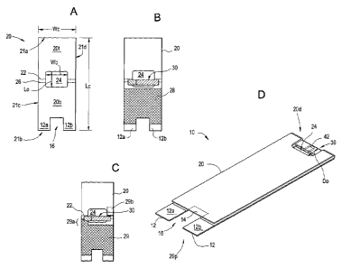
[0017] FIG. lA is a top view of a carrier in an unfolded configuration;
[0018] FIG. 1B is atop view of the carrier of FIG. IA having an adhesive and
an
electrochemical module ("ECM") disposed thereon;
[0019] FIG. 1C is a top view of the carrier of FIG. lA having another
embodiment of an
adhesive with an ECM disposed thereon;
[0020] FIG. 1D is a perspective view of the carrier and ECM of FIG. 1B, shown
in a folded
configuration to form a test strip assembly;
6a
CA 2833669 2017-06-13
CA 02833669 2013-10-18
WO 2012/143795 PCT/1B2012/000930
[0021] FIG. 2A is a side view of the ECM of FIG. 1B;
[0022] FIG. 2B is an exploded view of the ECM of FIG. 2A;
[0023] FIG. 3A is a perspective view of a carrier web shown in an unfolded
configuration and
having an adhesive disposed thereon, the carrier web forming multiple carriers
for forming
multiple test strip assemblies;
[0024] FIG. 3B is an enlarged perspective view of a portion of the carrier web
and adhesive
shown in FIG. 3A;
[0025] FIG. 3C is perspective view of the carrier web and adhesive of FIG. 3A
having an ECM
disposed across each opening in the carrier web;
[0026] FIG. 3D is a perspective view of the carrier web, adhesive, and ECMs of
FIG. 3B shown
partially folded;
[0027] FIG. 4A is a top view of another embodiment of an ECM;
[0028] FIG. 4B is a top view shown the ECM of FIG. 4A mounted onto a carrier,
shown in a
folded configuration, to form another embodiment of a test strip assembly;
[0029] FIG. 5 is a top view of a test strip assembly web, showing multiple
test strip assemblies
having a configuration as shown in FIG. 4B;
[0030] FIG. 6 is a top view of yet another embodiment of a test strip assembly
having multiple
ECMs;
[0031] FIG. 7 is a top view of one embodiment of an analyte measurement
device; and
[0032] FIG. 8 is a side view of a strip of electrochemical modules.
DETAILED DESCRIPTION
[0033] Certain exemplary embodiments will now be described to provide an
overall
understanding of the principles of the structure, function, manufacture, and
use of the devices,
systems, and methods disclosed herein. One or more examples of these
embodiments are
7
CA 02833669 2015-09-16
illustrated in the accompanying drawings. Those skilled in the art will
understand that the
devices and methods specifically described herein and illustrated in the
accompanying drawings
are non-limiting exemplary embodiments. The features illustrated or described
in connection
with one exemplary embodiment may be combined with the features of other
embodiments.
Such modifications and variations are intended to be included within the scope
of the present
disclosure.
[0034] The present invention generally provides an electrochemical sensing
apparatus having a
carrier that supports an electrochemical module, and that communicates between
electrodes on
the electrochemical module and an analyte measurement device. The carrier is
particularly
advantageous as it allows the electrochemical module to have a relatively
small size, while
providing a large surface area for ease of handling. The small size of the
electrochemical
module can reduce manufacturing costs, as less material is required to form
the electrodes. The
carrier also provides flexibility in design, allowing for various placement of
one or more
electrochemical modules, as well as allowing multiple sensing apparatus to be
formed as a unit.
[0035] FIGS. 1A-1D illustrate one exemplary embodiment of an electrochemical
sensing
apparatus, also referred to herein as a test strip assembly. As shown, the
test strip assembly 10
generally includes a carrier 20, shown in FIG. 1A, and an electrochemical
module 30 that is
mounted on the carrier 20, as shown in FIGS. 1B-1D. In general, the carrier 20
has dimensions
that are greater than the module 30, such that the carrier 20 serves as a
support to facilitate
handling of the module 30. A person skilled in the art will appreciate that
the test strip assembly
can have various configurations other than those shown, and can include any
combination of
features disclosed herein and known in the art. Moreover, each test strip
assembly can include
any number of electrochemical modules at various locations on the carrier for
measuring the
same and/or different analytes in a fluid sample.
[0036] Carrier
[0037] As indicated above, FIG. lA illustrates one embodiment of a carrier 20.
The carrier 20
can have various configurations, but it is typically in the form of one or
more rigid or semi-rigid
substrates having sufficient structural integrity to support the
electrochemical module 30 and to
allow handling and connection to an analyte measurement device, as will be
discussed in further
8
DOCSTOR 5295065\1
CA 02833669 2013-10-18
WO 2012/143795 PCT/1B2012/000930
detail below. The carrier can be formed from various materials, including
plastic or cardboard
materials. In an exemplary embodiment, materials that do not shed or that
exhibit relatively low
shedding of fibers are preferred. The substrate material typically is one that
is non-conductive.
The carrier material can also have any thermal coefficient of expansion,
including a low thermal
coefficient of expansion, as changes in the volume of the material during use
will not have any
effect on performance. In addition, the carrier materials can be inert and/or
electrochemically
non-functional, where they do not readily corrode over time nor chemically
react with ECM
material. The conductive material disposed on the carrier should be resistant
to corrosion where
the conductivity does not change during storage of the strip assemblies.
[0038] The shape of the carrier 20 can also vary. In the embodiment shown in
FIG. 1A, the
carrier 20 has a generally elongate rectangular shape with a length Le that is
greater than a width
We, the dimensions of which are discussed in further detail below. The carrier
20 includes first
and second terminal ends 21a, 21b, and first and second opposed sidewalls 21c,
21d extending
between the first and second terminal ends 21a, 21b. The carrier 20 can be
formed from separate
top and bottom portions, or as shown the carrier 20 can be configured to be
folded along a fold
line 22 to define top and bottom portions 20t, 20b that are in facing
relationship with one
another. A person skilled in the art will appreciate that the terms "top" and
"bottom" as used
herein are intended to serve as a reference for illustration purposes only,
and that the actual
position of the portions of the carrier will depend on the orientation of the
carrier. The top and
bottom portions 20t, 20b of the carrier 20 can allow an electrochemical
module, e.g., module 30,
to be mounted and engaged therebetween. The location of the fold line 22 can
vary. In the
illustrated embodiment, the fold line 22 is located offset from a mid-line of
the carrier 20 to
allow one of the top and bottom portions 20t, 20b of the carrier, e.g., the
bottom portion 20b in
FIG. 1A, to extend a distance beyond the terminal end of the other portion of
the carrier 20, e.g.,
the top portion 20t in FIG. 1A. Such a configuration facilitates connection to
an analyte
measurement device, as will be discussed further below. The carrier 20 can
also optionally
include one or more additional fold lines, which may facilitate spaced apart
positioning of the top
and bottom portions 20t, 20b, as is also discussed further below. The non-
conducting substrate
of the carrier can be kiss-cut at the intended fold line in order to
facilitate folding. If a sharp
blade is used to kiss-cut the substrate, sharp edges may results, in which
case it may be
preferable to firmly scribe a groove in the substrate using a blunt tool. This
will push aside the
9
CA 02833669 2013-10-18
WO 2012/143795 PCT/1B2012/000930
material of the substrate into smooth "banks" on either side of the groove in
such a way that the
folded carrier will not have sharp edges.
[0039] As further shown in FIG. 1A, the carrier 20 can also include at least
one hole or opening
extending therethrough for providing access to the electrochemical module, as
discussed further
below. The quantity of openings and the location of each opening can vary
depending on the
intended use, for example, whether more than one module will be present in a
carrier. In the
illustrated embodiment, the carrier 20 has a single opening 24 located
symmetrically across the
fold line 22. Such a configuration will allow the opening 24 to be positioned
along a perimeter
of the carrier 20 when the carrier 20 is folded, as shown in FIG. 1D. While
not shown, the
opening 24 can alternatively be positioned along any edge (e.g., along one of
the terminal ends
21a, 21b and/or the opposed sidewalls 21c, 21d) of the carrier 20, with
corresponding openings
extending through each of the top and bottom portions 20t, 20b. In other
embodiments, the
opening can extend through a mid-portion of the top and bottom portions 20t,
20b of the carrier
20 at a distance spaced apart from the perimeter or outer edge of the carrier
20.
[0040] The carrier 20 also includes one or more electrically conducting layers
to facilitate
communication between electrodes on the electrochemical module, discussed
below, and an
analyte measurement device. The electrically conducting layer(s) can be formed
from any
conductive material, including inexpensive materials, such as aluminum,
carbon, grapheme,
graphite, silver ink, tin oxide, indium oxide, copper, nickel, chromium and
alloys thereof, and
combinations thereof. However, precious metals that are conductive, such as
palladium,
platinum, indium tin oxide or gold, can optionally be used. The electrically
conducting layer(s)
can be disposed on all or portions of the carrier, but the particular
location(s) of the electrically
conducting layer(s) should be configured to electrically couple the
electrochemical module to the
analyte measurement device. In an exemplary embodiment, the entire portion or
a substantial
portion of the inwardly facing surface (i.e., the surface shown in FIG. 1A) of
the carrier 20 is
coated with the electrically conducting layer (not shown). As a result, each
of the top and
bottom portions 20t, 20b of the carrier 20 includes an electrically conducting
layer disposed
thereon. The carrier 20 can also include one or more electrical isolation
lines, e.g., referred to
herein as "breaks," formed in the electrically conducting layer to separate
the layer into a first
electrically conducting layer and a second electrically conducting layer that
is isolated from the
CA 02833669 2013-10-18
WO 2012/143795 PCT/1B2012/000930
first electrically conducting layer. The break(s) can be formed using various
techniques known
in the art, such as laser etching. If the electrically conducting layer is
formed by printing an ink,
then an unprinted area between the top and bottom portions 20t, 20b will
constitute a break. The
location of the break(s) can vary. For example, the break(s) can extend along
the fold line 22
such that the top portion 20t includes the first electrically conducting layer
which is electrically
isolated from the second electrically conducting layer on the bottom portion
20b. Thus, when
the carrier 20 is folded, as shown in FIG. 1D, the first electrically
conducting layer (not shown)
will be positioned on an inwardly facing surface of the top portion 20t of the
carrier 20, and the
second electrically conducting layer (not shown) will be positioned on an
inwardly facing
surface of the bottom portion 20b of the carrier 20 such that the first and
second electrically
conducting layers are in facing relationship with one another. As shown in
FIG. 1A, the
electrically conducting layer includes a first break formed along the fold
line 22, and a second
break 26 spaced a distance apart from the first break (fold line 22). The
breaks can be positioned
at various locations relative to the fold line 22, including on the same or
opposite sides of the
fold line 22. A person skilled in the art will appreciate that carrier 20 can
be manufactured to
include separate electrically conducting layers, rather than forming a single
layer with one or
more breaks. The separate layers can be formed from the same or different
materials.
[0041] In another embodiment, the electrically conducting layers can be
configured to prevent
"auto-starting" of the assays when one or both sidewalls 21c, 21d of the test
strip are
contaminated, e.g., with a salty solution such as perspiration from a user's
fingers. For example,
the electrically conducting layers can be formed by printing electrically
conductive inks (e.g.,
carbon, silver, grapheme, etc.), and the material can terminate at a distance
(e.g., 1 mm) from the
sidewalls 21c, 21d. Such a configuration will prevent contact between the
electrically
conducting material and a user's fingers when they grasp the test strip.
[0042] The electrically conducting layers can also be configured enable a
meter to distinguish
between different types of strips (e.g., to measure different analytes in a
liquid sample such as
glucose, lactate, cholesterol, hemoglobin, etc.). For example, two narrow
highly conducting
layers (e.g., printed with silver ink) can extend down from tabs 12a, 12b
towards the
electrochemical cavity, with a gap between the two narrow highly conducting
layers. A layer of
less conducting material (e.g., printed with carbon ink) can connect the two
narrow highly
11
CA 02833669 2015-09-16
conducting layers. When the resistance between the tabs 12a, 12b is measured,
the resistance
value will be dominated by the properties of the layer of less conducting
material. By varying
the thickness, width etc. of the layer of less conducting material, it will be
possible for the meter
to distinguish between different types of strips.
[0043] In order to maintain electrical separation between the first and second
electrically
conductive areas when the carrier 20 is folded, the carrier 20 can further
include a spacer layer,
which can be an adhesive layer. The spacer layer can function to maintain the
top and bottom
portions 20t, 20b of the carrier 20 at a distance apart from one another,
thereby preventing
electrical contact between the first and second electrically conducting layers
carried by the top
and bottom portions 20t, 20b. The spacer layer can also function as a double-
sided adhesive to
adhere the top and bottom portions 20t, 20b to one another, as well as to
secure the
electrochemical module 30 to the carrier. The spacer layer can be formed from
a variety of
materials, including a material with adhesive properties, or the spacer layer
can include a
separate adhesive used to attach the spacer to the carrier and optionally to
the electrochemical
module. Non-limiting examples of ways in which adhesives can be incorporated
into the various
test strip assemblies of the present disclosure can be found in U.S. Patent
Application Serial No.
12/570,268 of Chatelier et al., entitled "Adhesive Compositions for Use in an
Immunosensor"
and filed on September 30, 2009.
[0044] The spacer layer can have various shapes and sizes, and it can be
positioned on various
portions of the carrier 20. In the embodiment shown in FIG. 1B, a spacer layer
28 is positioned
on one side of the fold line 22 and extends over a substantial portion of the
inwardly facing
surface of the bottom portion 20b of the carrier 20. The spacer layer 28 can
terminate at or just
prior to the opening 24, so as to prevent the spacer layer 28 from extending
into the opening 24
and from contacting the electrochemical module when the carrier 20 is folded.
Termination at
the opening 24, however, can facilitate the formation of a seal around the
edge of the carrier
adjacent to the opening 24. The spacer layer 28 can also terminate a distance
from the second
terminal end 21b of carrier 20 so that, when the carrier is folded as shown in
FIG. 1D, the
exposed portion of the inwardly facing surface of the bottom portion 20b is
free from any
adhesive material.
12
DOCSTOR 5295065\1
CA 02833669 2013-10-18
WO 2012/143795 PCT/1B2012/000930
[0045] In another embodiment, shown in FIG. 1C, a spacer layer 29 is likewise
positioned to
cover a substantial portion of the inwardly facing surface of the bottom
portion 20b. In this
embodiment, however, the spacer layer 29 includes an extension portion 29a
that extends toward
or up to the fold line 22 adjacent to only one of the sidewalls, e.g., the
first sidewall 21e. In other
words, the extension portion 29a extends along only one side of the opening
24. The extension
portion 29a of the spacer layer 29 will thus be positioned between the
electrochemical module,
e.g., module 30, and the carrier 20 to attach the electrochemical module 30 to
the carrier 20 when
the carrier is folded. Preferably, the extension portion 29a is positioned to
contact an exterior
surface, e.g., the bottom exterior surface, of the electrochemical module 30,
and not one of the
inwardly facing surfaces as will be discussed below. Optionally, the spacer
layer 29 can also
include a separate portion 29b that is positioned on a side of the opening 24
opposite to the
extension portion 29a, and that is also positioned on an opposite side of the
fold line 22. This
separate portion 29b will thus contact the opposite exterior surface, e.g.,
the top exterior surface,
of the electrochemical module 30, as will be discussed below. A person skilled
in the art will
appreciate that the location of the spacer layer can vary.
[0046] In other aspects, the spacer layer 29 can be configured to have a size
and shape that
reduces fouling of punching/cutting tools with the adhesive. For example, the
edge of the
adhesive can be spaced a small distance (e.g., 0.5 mm) from the hole 24 to
prevent a punch tool
used to form the hole from coming into contact with the adhesive. Moreover, if
the adhesive is
printed, the edge of the adhesive can be spaced a small distance (e.g., 0.5
mm) from the sidewalls
21c, 21d to prevent a cutting tool from coming into contact with the adhesive
during a
singulation step (i.e., when multiple strips are cut to form singular strips).
[0047] The carrier 20 can also include electrical contacts for coupling to an
analyte measurement
device. The electrical contacts can be located anywhere on the carrier 20, In
the illustrated
embodiment, the second terminal end 21b of the carrier 20 includes first and
second contacts 12,
14 configured to establish a connection between first and second electrodes,
respectively, on the
module 30 (discussed below) and an analyte measurement device. As best shown
in FIG. 1D,
the first contact 12 is in the form of first and second tabs 12a, 12b located
on the terminal end
21b of the bottom portion 20b of the carrier 20. When the carrier is folded,
the tabs 12a, 12b will
extend a distance beyond the terminal end 21a of the top portion 20t of the
carrier 20, as shown
13
CA 02833669 2015-09-16
in FIG. 1D. The tabs 12a, 12b can be formed by a cut-out or u-shaped notch 16
extending into
the second terminal end 21b of the bottom portion 20b of the carrier 20 at a
substantial mid-
portion thereof. The cut-out 16 is also effective to expose the first
electrically conducting layer
on the inwardly facing surface of the top portion 20t of the carrier 20,
thereby forming the
second contact 14 (shown in phantom in FIG. 1D) for connecting the first
electrically conducting
layer to an analyte measurement device. A person skilled in the art will
appreciate that the
electrical contacts can have a variety of configurations other than those
illustrated. For example,
U.S. Patent No. 6,379,513 discloses another embodiment of an electrochemical
cell connection
means.
[0048] The configuration of the electrically contacts can allow a measurement
device to
recognize a test strip by sensing a decrease in resistance between the meter
tangs that connect to
the tabs 12a, 12b on the carrier, as shown in FIG. 1D. As a further feature,
tab 14 in FIG. 1D can
be made to have a width that allows two additional meter tangs to electrically
connect to the tab
14. This allows the meter to ensure that sufficient electrical contact is made
with tab 14 before
the user is prompted to apply a liquid sample to the cavity 42 in the
electrochemical module 30.
Such a configuration can prevent a "waiting for sample" error which can be
seen in systems
which do not ensure good electrical contact prior to initiating an
electrochemical assay. In
another embodiment, where tab 14 does not have a width sufficient to connect
with two meter
tags, electrical contact between the meter and tab 14 can still be monitored
by performing a "dry
capacitance" measurement before the liquid sample is applied to the
electrochemical cavity 42.
The capacitance measurement must fall within the range expected for a dry
strip before the user
is prompted to apply the liquid sample to the cavity 42 in the electrochemical
module 30.
[0049] The carrier can be configured to couple to a variety of analyte
measurement devices
having various configurations. In general, the measurement device can include
a processor,
which may include one or more control units configured for performing
calculations capable of
calculating a correction factor in view of at least one measured or calculated
parameter as well as
configured for data sorting and/or storage. The microprocessor can be in the
form of a mixed
signal microprocessor (MSP) such as, for example, a member of the Texas
Instruments MSP 430
family. In addition, the microprocessor can include volatile and non-volatile
memory. In
another embodiment, many of the electronic components can be integrated with
the
14
DOCSTOR: 5295065\1
CA 02833669 2013-10-18
WO 2012/143795 PCT/1B2012/000930
microcontroller in the form of an application specific integrated circuit.
[0050] The dimensions of the carrier can vary significantly depending on the
configuration of
the analyte measurement device, as well as the quantity and configuration of
the electrochemical
module(s) on the test strip assembly. In the embodiment shown in FIG. 1A, and
by way of non-
limiting example, the carrier 20 can have a width We that is in the range of
about 0 mm to 4 mm
larger than the width of the electrochemical module. For example, the width Wo
of the carrier 20
can be in the range of about 5 mm to 50 mm. Also by way of non-limiting
example, the carrier
20 can have a length Lc in the unfolded configuration that is in the range of
about 20 mm to 200
mm, and more preferably 30 mm to 50 mm. The dimensions of the opening(s) in
the carrier 20
can also vary, but in an exemplary embodiment the opening 24 has a generally
oval or
rectangular configuration with a width Wo as measured in a direction extending
between the
opposed sidewalls 21c, 21d that is in the range of about 3 mm to 49 mm. The
length Lo (in the
unfolded configuration) of the opening can be in the range of about 0 to 6 mm
larger than twice
the length of the electrochemical module (the factor of two is required since
the carrier web will
be folded). For example, the length Lo of the opening can be in the range of
about 3 to 30 mm.
When the carrier 20 is folded as shown in FIG. 1D, the opening 24 will have a
depth Do that is
one half of the length Lo, as measured from the fold line 22 inward. A person
skilled in the art
will appreciate that the terms "about" and "approximately" as used herein for
any numerical
values or ranges indicate a suitable dimensional tolerance that allows the
part or collection of
components to function for its intended purpose as described herein.
[0051] Electrochemical Module
[0052] The electrochemical module (ECM) can also have a variety of
configurations and various
electrochemical cell sensors known in the art can be used. In one embodiment,
the module can
include multiple electrodes and a reagent layer, and the module can be
configured to receive and
react with an analyte in a fluid sample. The multiple electrodes can be
configured in any suitable
configuration, such as adjacent one another and in the same plane, or facing
one another in an
opposed spaced apart relationship. The module can be mounted onto a carrier,
such as carrier
20, such that the carrier serves as a support for the module and facilitates
handling. As indicated
above, the carrier can also electrically couple the module to an analyte
measurement device.
CA 02833669 2013-10-18
WO 2012/143795 PCT/1B2012/000930
[0053] While the module can have various configurations, in the embodiment
shown in FIGS.
2A-2B, the electrochemical module 30 generally includes a first insulating
layer 32 carrying a
first electrode 36, a second insulating layer 34 carrying a second electrode
38 that is in facing
relationship with the first electrode 36 on the first insulating layer 32, and
one or more spacers
40a, 40b maintaining the first and second electrodes 36, 38 at a distance
apart from one another
to define a cavity or chamber 42 therebetween for receiving a fluid analyte.
For ease of
reference, the first insulating layer 32 is also referred to herein as the top
insulating layer, and the
second insulating layer 34 is also referred to as the bottom insulating layer.
The terms "top" and
"bottom" are merely used to describe the illustrated orientation and are not
intended to limit the
layers to a particular orientation. The illustrated electrochemical module 30
can also include a
reagent 44 disposed on one of the first and second electrodes, e.g., the
second electrode 38, and
disposed between the spacers 40a, 40b and within the chamber 42 for reacting
with an analyte.
A person skilled in the art will appreciate that the electrochemical module 30
can have a variety
of configurations, including having other electrode configurations, such as co-
planar electrodes.
[0054] The first and second insulating layers 32, 34 can each have various
shapes and sizes, and
the particular configuration of the insulating layers 32, 34 can vary
depending on the particular
configuration of the carrier 20. In the illustrated embodiment, the first and
second insulating
layers 32, 34 each have a generally rectangular shape. The insulating layers
32, 34 can be
formed from various materials, but in an exemplary embodiment the insulating
layers 32, 34 are
formed from a material having a small coefficient of thermal expansion such
that the insulating
layers 32, 34 do not adversely affect the volume of the reaction chamber 42,
as will be discussed
in detail below. In one exemplary embodiment, at least one of the insulating
layers, e.g., the first
layer 32, can be formed from a transparent material to allow visualization of
fluid flow into the
reaction chamber. Suitable materials include, by way of non-limiting example,
plastics (such as
PET, PETG, polyimide, polycarbonate, polystyrene), ceramic, glass, adhesives.
[0055] As indicated above, each insulating layer 32, 34 can carry an electrode
36, 38. As shown
in FIG. 2A, an inwardly facing surface of the first insulating layer 32
carries the first electrode
36, and an opposing inwardly facing surface of the second insulating layer 34
carries the second
electrode 38. The electrodes 36, 38 can each be formed from a layer of
conductive material,
such as gold, palladium, carbon, silver, platinum, tin oxide, iridium, indium,
and combinations
16
CA 02833669 2013-10-18
WO 2012/143795 PCT/1B2012/000930
thereof (e.g,, indium doped tin oxide). Carbon in the form of graphene may
also be used. The
conductive material can be deposited onto the insulating layers 32, 34 by
various processes, such
as sputtering, electroless plating, thermal evaporation and screen printing.
In an exemplary
embodiment, the reagent-free electrode, e.g., the first electrode 36, is a
sputtered gold electrode,
and the electrode containing the reagent 44, e.g., the second electrode 38, is
a sputtered
palladium electrode. As discussed in further detail below, in use one of the
electrodes can
function as a working electrode and the other electrode can function as the
counter/reference
electrode.
[0056] When the electrochemical module 30 is assembled, the first and second
insulating layers
32, 34, and thus the first and second electrodes 36, 38, can be held together
at a spaced distance
apart by one or more spacers. As shown in FIG. 2B, the electrochemical module
30 includes
first and second spacers 40a, 40b, also referred to as adhesives. The
illustrated spacers 40a, 40b
each have a generally rectangular configuration with a length Ls that can be
substantially equal to
a length Li of the insulating layers 32, 34, and a width Ws that is
significantly less than a width
Wi of the insulating layers 32, 34. However, the shape and size, as well as
the quantity, of the
spacers 40a, 40b can vary significantly. As shown, the first spacer 40a is
positioned adjacent to a
first terminal end 34a of the second/bottom insulating layer 34, and the
second spacer 40b is
positioned near a mid-portion of the second/bottom insulating layer 34 such
that a space or gap is
defined between the first and second spacers 40a, 40b. The second terminal end
32b of the
first/top insulating layer 32 can be positioned in substantial alignment with
an edge of the second
spacer 40b farthest from the first spacer 40a, such that the first terminal
end 32a of the first/top
insulating layer 32 extends a distance beyond the first terminal end 34a of
the second/bottom
insulating layer 34. As a result, the second terminal end 34b of the
second/bottom insulating
layer 34 will extend a distance Di beyond the second terminal end 32b of the
first/top insulating
layer 32, as shown in FIG. 2A. The first and second insulating layers 32, 34
can thus be
positioned offset from one another, thereby exposing an inwardly facing
portion of each of the
first and second electrodes 36, 38. A person skilled in the art will
appreciate that the particular
configuration, including the shape, orientation, and location of the spacer(s)
and the insulating
layers relative to one another can vary.
[0057] As indicated above, the spacers 40a, 40b and electrodes 36, 38 define a
space or gap, also
17
CA 02833669 2015-09-16
referred to as a window, therebetween which forms an electrochemical cavity or
reaction
chamber 42 for receiving a fluid sample. In particular, the first and second
electrodes 36, 38
define the top and bottom of the reaction chamber 42, and the spacers 40a, 40b
define the sides
of the reaction chamber 42. The gap between the spacers 40a, 40b will result
in the opposed
sidewalls of the module 30 having openings or inlets extending into the
reaction chamber 42.
The fluid sample can thus be loaded through the side openings.
[0058] As further shown in FIG. 2A, the reaction chamber 42 can also include a
reagent 44
disposed on at least one of the electrodes, e.g., the second electrode 38.
Alternatively, the
reagent layer can be disposed on multiple faces of the reaction chamber 42.
The reagent 44 can
he formed from various materials, including various mediators and/or enzymes.
Suitable
mediators include, by way of non-limiting example, ferricyanide, ferrocene,
ferrocene
derivatives, osmium bipyridyl complexes, and quinone derivatives. Suitable
enzymes include,
by way of non-limiting example, glucose oxidase, glucose dehydrogenase (GDH)
based on
pyrroloquinoline quinone (PQQ) co-factor, GDH based on nicotinamide adenine
dinucleotide co-
factor, and FAD-based GDII [E.C.1.1.99.10]. One exemplary reagent formulation,
which would
be suitable for making the reagent 44, is described in pending U.S. Patent No.
7,291,256, entitled
"Method of Manufacturing a Sterilized and Calibrated Biosensor-Based Medical
Device." The
reagent 44 can be formed using various processes, such as slot coating,
dispensing from the end
of a tube, ink jetting, and screen printing. Such processes are described, for
example, in the
following U.S. Patents: 6,749,887; 6,869,441; 6,676,995; and 6,830,934. While
not discussed in
detail, a person skilled in the art will also appreciate that the various
electrochemical modules
disclosed herein can also contain a buffer, a wetting agent, and/or a
stabilizer for the biochemical
component.
[0059] The size of the electrochemical module 30 and its components can vary.
For example, in
one embodiment, the first and second insulating layers 32, 34 can each have
substantially the
same size, with a length L, and width W, that is less than a length Le and
width W, of the carrier
20. By way of non-limiting example, the insulating layers 32, 34 can each have
a width W, that
is at least twice the length L. For example, the width W, can be in the range
of about 3 mm to 48
mm, and more preferably about 6 mm to 10 mm, and a length L, in the range of
about 0.5 mm to
18
DOCSTOR. 5295065\1
CA 02833669 2013-10-18
WO 2012/143795 PCT/1B2012/000930
20 mm, and more preferably 1 mm to 4 mm. The distance De between the top
electrode 36 and
the bottom electrode 38, as well as the dimensions of the spacers 40a, 40b,
can also vary
depending on the desired volume of the reaction chamber 42. In an exemplary
embodiment, the
reaction chamber 42 has a small volume. For example, the volume can range from
about 0.1
microliters to about 5 microliters, preferably about 0.2 microliters to about
3 microliters, and
more preferably about 0.2 microliters to about 0.4 microliter. To provide the
small volume, the
gap between the spacers 40a, 40b can have an area ranging from about 0.005 cm2
to about 0.2
cm2, preferably about 0.0075 cm2 to about 0.15 cm2, and more preferably about
0.01 cm2 to
about 0.08 cm2, and the thickness of the spacers 40a, 40b (i.e., the height HO
can range from
about 1 micron to 500 microns, and more preferably about 10 microns to 400
microns, and more
preferably about 40 micros to 200 micros, and even more preferably about 50
microns to 150
microns. As will be appreciated by those skilled in the art, the volume of the
reaction chamber
42, the area of the gap between the spacers 40a, 40b, and the distance between
the electrodes 36,
38 can vary significantly.
[0060] Test Strip Assembly
[0061] Various techniques can be used to prepare a test strip assembly having
both a carrier and
an electrochemical module. Referring back to FIGS. 1A-1D, in one embodiment a
single test
strip assembly 10 can be formed by providing a carrier, e.g., carrier 20, and
placing a spacer
layer 28 or 29 and an electrochemical module 30 onto the carrier 20. The
electrochemical
module 30 is preferably mounted onto the carrier 20 in such a way as to allow
the carrier 20 to
function as a support for handling the apparatus, while also allowing easy
access to the reaction
chamber 42. While the particular location of the module 30 relative to the
carrier 20 can vary
depending on the configuration of the module 30, the quantity of modules 30
mounted onto the
carrier 20, and the configuration of the carrier 20, in the illustrated
embodiment the module 30 is
mounted on the carrier 20 such that the module 30 extends across the opening
24 and is
positioned along or adjacent to one side of the fold line 22. The opposed
terminal ends of the
module 30 are thus in contact with the carrier 20, while a central or mid-
portion of the module 30
is not in contact with and is spaced apart from the carrier 20. The spacer
layer 28 or 29 can
likewise be positioned at various locations on the carrier 20. As explained
above, the spacer
layer 28 or 29 can function as an adhesive to secure the module 30 between the
top and bottom
19
CA 02833669 2013-10-18
WO 2012/143795 PCT/1B2012/000930
portions 20t, 20b of the carrier 20, thus preventing movement of the module 30
relative to the
carrier 20. While FIG. 1B illustrates the spacer 28 positioned a distance
apart from the module
30 such that the spacer 28 does not contact the module 30 even when the
carrier 20 is folded, the
spacer can have other configurations such as the configuration shown in FIG.
1C in which the
spacer 29 has portions 29a, 29b that extend over at least the terminal end
portions of the module
30 to adhere the module 30 directly to the carrier 20.
[0062] Once the module 30 and spacer 28 or 29 are positioned on the carrier
20, the carrier 20
can be folded along the fold line 22, as shown in FIG. 1D, thereby adhering
the top and bottom
portions 20t, 20b to one another and thereby engaging the electrochemical
module 30 between
the top and bottom portions 20t, 20b. When folded, the carrier 20 will have a
proximal end 20p
with the first and second electrical contacts 12, 14, and a distal end 20d
having the module 30
located thereon. The module 30 can be positioned adjacent to or along the
terminal distal edge
or perimeter of the carrier 20 such that one side of the opening extending
into the reaction
chamber 42 is positioned along the perimeter to allow for side loading of a
fluid sample into the
reaction chamber 42. The other side of the module 30, e.g., the proximal side,
is spaced a
distance apart from the inner edge of the opening 24 to create a gap. The gap
between the carrier
and the module allows a fluid sample to flow into the reaction chamber 42
without flowing into
the carrier 20, e.g., between the top and bottom portions 20t, 20b. As used
herein, the term
"proximal" indicates that a reference structure is close to the test meter and
the term "distal"
indicates that a reference structure is farther away from the test meter.
[0063] When fully assembled, as shown in FIG. 1D, the inwardly facing surface
of the top
electrode 36 will directly contact and electrically connect with the inwardly
facing surface of the
bottom portion 20b of the carrier 20, and the inwardly facing surface of the
bottom electrode 38
will directly contact and electrically connect with the inwardly facing
surface of the top portion
20t of the carrier 20. The connection results from the offset configuration of
the insulating layers
32, 34 and electrodes 36, 38, as shown in FIG. 2A. In particular, FIG. 2B
shows that the
connection will occur at the first terminal end 32a of the first/top
insulating layer 32 that extends
a distance beyond the first terminal end 34a of the second/bottom insulating
layer 34, and at the
second terminal end 34b of the second/bottom insulating layer 34 that extends
a distance beyond
the second terminal end 32b of the first/top insulating layer 32. The first
electrode 36 is shielded
CA 02833669 2013-10-18
WO 2012/143795 PCT/1B2012/000930
from contacting the top portion 20t of the carrier 20 by the first insulating
layer 32, and the
second electrode 38 is shielded from contacting the bottom portion 20b of the
carrier by the
second insulating layer 34. The first electrode 36 will therefore communicate
with an analyte
measurement device through the bottom portion 20b of the carrier and through
the first electrical
contact 12, e.g., tabs 12a and 12b, and the second electrode 38 will
communicate with the
analyte measurement device through the top portion 20t of the carrier and
through the second
electrical contact 14. The spacer layer will maintain electrical separation
between the top and
bottom portions 20t, 20b of the carrier 20.
[0064] The assembled dimensions of the ECM and the test strip assembly can
vary, but in one
exemplary embodiment the ECM has a width of about 10 mm and a length (measured
in a
proximal-distal direction) of about 2 mm, and the carrier or test strip
assembly has a width of
about 12 nun and a length (measured proximal-distal direction) of about 40 mm.
The
dimensions of the carrier are thus significantly larger than the dimensions of
the ECM.
[0065] Exemplary Manufacturing Process
[0066] In one exemplary embodiment, a test strip assembly can be manufactured
by applying a
coating of conducting carbon ink to a 76 mm wide web of glossy cardboard, PET
or
polypropylene having an appropriate stiffness. The thickness of the coating
should be sufficient
to reduce the surface resistance such that the overall resistance of the
connector track is less than
200 Ohms. The conducting layer on the carrier can be etched downweb with a
laser or a
mechanical scriber at a location 40 mm from one edge such that the web is
divided into two
electrically isolated functional regions, e.g., top portion 20t and bottom
portion 20b. For a
carrier web having multiple test strip assemblies, e.g., a multi-panel test
strip assembly, the web
can also be etched in a crossweb direction at 20 mm intervals to separate each
test strip
assembly. A spacer or adhesive layer, e.g., spacer 128, covered by a release
liner can be
laminated to the web, as shown in FIG. 3C, such that one of its edges is 4 mm
from the terminal
end of the bottom portion 20b of the carrier web and the other edge is about 5
mm above the
center line of the carrier web. Referring back to FIG. 3C, note that the
center line can
correspond to the location of the fold line 122. Holes 124, having a diameter
of 8 mm, can be
punched into the carrier web in a downweb direction along the etched line at
12 mm intervals
21
CA 02833669 2013-10-18
WO 2012/143795 PCT/1B2012/000930
(center-to-center), and slots can be punched in the bottom (proximal) end. For
a multi-panel test
strip assembly, the holes can be in the middle of each 20 mm section. A 34 nun
wide track of
double-sided adhesive separator (about 95 2 micrometers height with 50
micrometer release
liners) can be kiss-cut and the waste removed in such a way that there are 4
repeating patterns,
shown in part in FIG. 8, which consist of (1) a 1.2 min wide cavity (labeled
"a" in FIG. 8) in the
middle that will form an electrochemical cavity in a later step, and (2) a 2.4
mm wide spacer
section separator (labeled "b" in FIG. 8) on each side that will form the
walls of the
electrochemical cavity in a further step. The term kiss-cut can be used when
referring to a partial
cut through a laminate structure. For example, the laminate structure
including an Au-PET layer,
an adhesive spacer layer, and a Pd-PET layer can be kiss-cut such that only
the Au-PET layer or
Pd-PET layer is cut. The remaining separator will form a reagent-free cavity
(2 mm on each
side, labeled "c" in FIG. 8) that will expose overhanging electrodes in a
further step. A 32 mm
wide track of PET filled with barium sulfate particles is sputtered with 60 nm
of Pd, brought into
contact with 0.3 mM MESA in water for 20 seconds, and then the excess liquid
is blown off with
an air knife. Four strips of reagent (identical or different) are applied to
the Pd electrode, 8 mm
apart (center-to-center). The double-sided adhesive separator is bonded to the
Pd electrode in
such a way that each 1.2 mm wide cavity overlays a reagent stripe. A 32 mm
wide track of clear
PET is sputtered with 30 nm of Au, brought into contact with 0.3 mM MESA in
water for 20
seconds, and then the excess liquid is blown off with an air knife. The Pd-
separator-Au tri-
laminate is kiss-cut through the electrode layer only from two directions, as
shown by the arrows
in FIG. 8, in such a way that either the Pd or the Au extends past the edge of
the spacer layer and
the other electrode layer. The different tracks of tri-laminate can be
separated to form four
electrochemical modules, two of which are shown in FIG. 8 and labeled A and B,
with only a
portion of the remaining two being shown. The total width of each of the
modules will be 2 mm
(section c, upper electrode) + 2.4 nun (section b, trilaminate) + 1.2 mm
(section a, cavity plus
reagent) + 2.4 mm (section b, trilaminate) + 2 mm (section c, lower
electrode), for a total of 10
mm. This is larger than the total length of 32 divided by 4 (about 8 ram)
because of the separate
exposed regions of upper and lower electrodes. Each module of tri-laminate is
cut into 2 mm
long sensors and placed on the carrier as described above. One way to achieve
this is to push a
leading edge of the tri-laminate into a slot on a wheel and cut off the 2 mm
wide sensor. The
wheel would then rotate so that another slot would receive the leading edge of
the tri-laminate
22
CA 02833669 2013-10-18
WO 2012/143795 PCT/1B2012/000930
web and another piece of 2 mm wide sensor would be cut off, etc. The carrier
web would
advance past the opposite end of the wheel and receive each 2 mm wide sensor
in such a way
that the appropriate edge of the electrochemical cavity coincides with the
middle of a hole in the
carrier. For the multi-analyte test strip assembly, the track order along the
carrier would be 1-2-
3-4, 1-2-3-4, etc., with a separate rotating wheel for each reagent. Since
each small ECM is 10
mm wide and each carrier is 12 mm wide, there will be sufficient gap between
each edge of the
ECM and carrier so that the cutting machine does not disturb the ECM in the
final "singulation"
step. The carrier is folded at a line which was laser etched downweb, bonded
to the double sided
adhesive separator, optionally printed with a logo and other required
information, and then
chopped as appropriate. The folding process can either be done continuously in
a web process,
or the web can be chopped into cards which can then be folded. For the multi-
analyte test strip
assembly, a set of four ECMs can be chopped into a single card. If all
reagents are identical and
an average value is required, then each card can contain two or four ECMs.
Alternatively, the
web can be processed for the simplest application with single, identical
sensors.
[0067] Other Embodiments
[0068] While one embodiment of a test strip assembly 10 is shown in FIG. 1D,
FIGS. 3A-4
provides various other embodiments of test strip assemblies. A person skilled
in the art will
appreciate that, while not specifically discussed, the test strip assemblies
set forth in FIGS. 3A-4
can include any combination of features discussed above with respect to FIGS.
1A-1D and/or
other features known in the art.
[0069] In one embodiment, a carrier web having multiple test strips assemblies
can be formed.
Such a configuration allows for mass production of multiple test strip
assemblies. Each test strip
assembly can simply be cut or otherwise removed from the carrier web prior to
use. For
example, the carrier web can include scored regions between each test strip
assembly to facilitate
removal of a test strip assembly without the need for scissors or another
cutting mechanism.
Alternatively, an analyte measurement device can have multiple terminals
configured to accept a
carrier web having multiple electrochemical modules. Such a configuration
could allow for
multiple analytes to be tested simultaneously. Such a configuration could, in
other embodiments,
allow multiple readings of a single analyte to be taken, thus allowing the
device to exclude
23
CA 02833669 2013-10-18
WO 2012/143795 PCT/1B2012/000930
outliers and display an average. This would provide a robust estimate of the
analyte
concentration and can enhance both the precision and the accuracy of the
measurement.
[0070] While the carrier web can have various configurations, FIG. 3A
illustrates one
embodiment of a carrier web 100 having a generally elongate rectangular
configuration. The
carrier web 100 can have the same length L as the length L of the carrier 20
discussed above
with respect to FIG. 1A, however the width W,, of the carrier web 100 can be
multiple times the
width We of the carrier 20 discussed with respect to FIG. 1A. In particular,
the width Wv,, of the
carrier web 100 preferably corresponds to the width W, of the carrier of FIG.
1A times the
number of carriers that the carrier web 100 is to contain. For example, if the
carrier web 100 is
configured to produce ten (10) carriers, and thus ten test strip assemblies,
then the width Ww of
the carrier web 100 will be about ten (10) times the width We of a single
carrier. A person
skilled in the art will appreciate that the particular dimensions of the
carrier web 100 can vary.
[0071] As further shown in FIGS. 3A and 3B, the carrier web 100 can include
multiple openings
124 formed therein, each opening 124 having a configuration similar to the
openings 24
previously discussed above with respect to FIG. 1A. As shown, the openings 124
can be spaced
a distance apart from one another and longitudinally aligned along an intended
fold line 122 on
the carrier web 100. The carrier web 100 can also include an adhesive or
spacer 128 disposed on
various portions of the carrier web 100. In the illustrated embodiment, the
spacer 128 is
positioned on one side of the intended fold line 122. The spacer 128 can
include a portion 128a
that extends along one side of each opening 124 for contacting a bottom
surface of the
electrochemical module, e.g., module 130, when mounted thereon. The spacer 128
can also
include a separate, second portion 128b that is positioned on an opposite side
of each opening
124, and on an opposite side of the fold line 122 such that the second portion
128b of spacer 128
contacts a top surface of the electrochemical module 130. When the carrier web
100 is folded,
the spacer 128 will connect the top and bottom portions of the carrier web 100
to one another,
while maintaining the top and bottom portions 100t, 100b at a spaced apart
distance from one
another. The portions of spacer 128 that extend along each side of the
openings 124 will adhere
to and affix each electrochemical module 130 to the carrier web 100, thereby
maintaining the
modules 130 in a fixed position relative to the carrier web 100.
24
CA 02833669 2013-10-18
WO 2012/143795 PCT/1B2012/000930
[0072] FIG. 3C illustrates the carrier web 100 of FIGS. 3A and 3B having an
electrochemical
module 130 mounted to extend across each opening 124 in the web. Each module
130 on the
web 100 can have a configuration as previously explained. In other
embodiments, the modules
130 on the carrier web 100 can differ from one another, e.g., to allow
different analytes to be
tested. A person skilled in the art will appreciate that the configuration of
the carrier web 100
and modules 130 mounted thereon, as well as the location of each module 130 on
the carrier web
100, can vary significantly depending on the intended use.
[0073] FIG. 4A illustrates another embodiment of an electrochemical module
230, and FIG. 4B
illustrates the electrochemical module mounted 230 onto a carrier 220 to form
a test strip
assembly 200. In this embodiment, the electrochemical module 230 has a curved
or bent
configuration to position the electrochemical cell or reaction chamber 242 a
farther distance
apart from the inner edge of the opening 224 in the carrier 220. In
particular, the electrochemical
module 230 has a configuration similar to that described above with respect to
FIGS. 2A and 2B,
however the module 230 includes bent or angled end portions. As shown, a
portion of the
module 230 which contains the reaction chamber 242, e.g,, a mid-portion 230a,
extends along a
central axis LI, and two terminal end portions 230b, 230c each extend along
axes L2, L3 that
extend at an angle a relative to the central axis L1 of the mid-portion 230a.
The central axis L1
can also extend orthogonal to a direction of flow of a sample into the
reaction chamber 242. The
angle a between each end portion 230b, 230c and the mid-portion 230a can vary.
For example,
in the illustrated embodiment the angle a is an acute angle, and more
particularly is greater than
0 degrees and less than 90 degrees. For example, the angle a can be about 45
degrees. Each
terminal end portion 230b, 230c is preferably oriented to extend away from the
central axis Li of
the mid-portion 230a in the same direction. Such a configuration allows the
terminal end
portions 230b, 230c to be mounted onto the carrier 220 on opposed sides of the
opening 242, as
shown in FIG. 4B, with the mid-portion 230a positioned a distance apart from
the inner edge of
the opening 224. The distance dean vary depending on the length of the end
portions 230b,
230c, but in an exemplary embodiment the electrochemical module 230 is
configured such that
the distal-most edge 230d of the module 230 is positioned distal to the distal-
most edge 220d of
the carrier 220. As a result, the distance d between the proximal edge of the
module 230 and the
proximal inner edge of the carrier 220 at the opening 224 is increased to help
prevent fluid from
flowing from the reaction chamber 242 into the carrier 220.
CA 02833669 2013-10-18
WO 2012/143795 PCT/1B2012/000930
[0074] FIG. 5 illustrates multiple electrochemical modules 230, having the
same configuration
as the module of FIG. 4A, mounted onto a carrier web 300, similar to the
carrier web 100
discussed above with respect to FIG. 3D. A person skilled in the art will
appreciate that the web
and the modules can have a variety of configurations, and can include any
combination of
features disclosed herein arid/or known in the art.
[0075] FIG. 6 illustrates another embodiment of a test strip assembly 400,
shown fully
assembled in a folded configuration. In this embodiment, the assembly 400
includes multiple
electrochemical modules 430a, 430b, 430c mounted at various locations on a
single carrier 420.
In particular, the carrier 420 has a configuration similar to the carrier 20
of FIG. 1A, however, in
addition to the distal opening 424b, the carrier 420 includes first and second
opposed side
openings 424a, 424c extending through each of the top and bottom portions of
the carrier 420.
This allows three electrochemical modules 430a, 430b, 430c to be mounted onto
the carrier 420
between the top and bottoms portions of the carrier 420. Each module 430a,
430b, 430c can be
positioned to extend across an opening 424a, 424b, 424c, as shown. Each module
430a, 430b,
430c can be configured to measure the same analyte in a fluid sample, or to
measure different
analytes. Multiple electrical isolation lines or "breaks" 426 can be formed in
the carrier to
electrically isolate each module 430a, 430b, 430c and allow the carrier 420 to
provide separate
electrically connections between each module 430a, 430b, 430c and different
electrical
connections on an analyte measurement device. A person skilled in the art will
appreciate that
each module can have various configurations, including a configuration similar
to the
embodiment of FIG. 4A, and that the modules can be mounted at various
locations on the carrier
420, or on a carrier web. The electrical contacts for coupling to an analyte
measurement device
can also have a variety of configurations.
[0076] Use
[0077] The test strip assemblies disclosed herein are suitable for use in the
determination of a
wide variety of analytes in a wide variety of samples, and are particularly
suited for use in the
determination of analytes in whole blood, plasma, serum, interstitial fluid,
or derivatives thereof.
By way of non-limiting example, the electrochemical modules can be configured
as a glucose
sensor, a lactate sensor based on lactate dehydrogenase, a lactate
dehydrogenase sensor which
26
CA 02833669 2015-09-16
includes lactate (to report on tissue damage), a ketone body sensor based on
13-hydroxy-butyrate
dehydrogenase, a cholesterol sensor based on cholesterol oxidase, a hemoglobin
sensor which
includes a cytolytic agent such as deoxycholate, and an immunosensor which
contains an
antibody and/or an antigen.
[0078] In use, a test strip assembly can be loaded into an analyte measurement
device, such as a
meter. An audible confirmation of connection can optionally be provided. The
test meter will
connect to the first and second electrical connections on the test strip
assembly to form a
complete circuit. An example is shown in FIG. 1D where contacts 12a and 12b
can be used to
recognize strip insertion into the meter. The test meter can measure the
resistance or electrical
continuity between the electrical contacts on the test strip assembly to
determine whether the test
strip is electrically connected to the test meter. The test meter can use a
variety of sensors and
circuits to determine when a test strip is properly positioned with respect to
the test meter. In
one embodiment, a circuit disposed in the test meter can apply a test
potential and/or a current
between first electrical contact and second electrical contact. Once the test
meter recognizes that
a test strip assembly has been inserted, the test meter turns on and initiates
a fluid detection
mode. In one embodiment, the fluid detection mode causes the test meter to
apply a constant
current of about 1 microampere between the first electrode and the second
electrode. An
example is shown in FIG. 1D where the flow of current between contact 14 and
contact 12 can
be used to detect fluid in the strip. Because the test strip assembly is
initially dry, the test meter
measures a maximum voltage, which is limited by the hardware within the test
meter. The fluid
sample, such as a physiological fluid or control solution, can be delivered to
the sample reaction
chamber 42 for electrochemical analysis via the opening until the fluid sample
fills the sample
reaction chamber. When the fluid sample bridges the gap between the first and
second
electrodes, the test meter will measure a decrease in measured voltage (e.g.,
as described in U.S.
Patent No. 6,193,873), which is below a predetermined threshold causing the
test meter to
automatically initiate the analyte test, e.g., a glucose test.
[0079] It should be noted that the measured voltage may decrease below a pre-
determined
threshold when only a fraction of the sample reaction chamber has been filled.
A method of
automatically recognizing that a fluid was applied does not necessarily
indicate that the sample
27
DOCSTOR. 5295065\1
CA 02833669 2015-09-16
reaction chamber has been completely filled, but can only confirm a presence
of some amount of
fluid in the sample reaction chamber. Once the test meter determines that a
fluid has been
applied to the test strip assembly, a short, but non-zero amount of time may
still be required to
allow the fluid to completely fill the sample reaction chamber. At this point,
the meter can apply
a series of electrical potentials, measure the electrical current versus time,
and use an algorithm
to calculate the concentration of analyte in the test liquid.
[0080] By way of non-limiting example, FIG. 7 illustrates one embodiment of an
analyte
measurement device, e.g., a diabetes management unit (DMU) 500. The DMU 500
generally
includes a housing 502, user interface buttons 504, a display 506, and a test
strip port opening
508. The user interface buttons 504 can be configured to allow the entry of
data, navigation of
menus, and execution of commands. Data can include values representative of
analyte
concentration, and/or information, which are related to the everyday lifestyle
of an individual.
Information, which is related to the everyday lifestyle, can include food
intake, medication use,
occurrence of health check-ups, and general health condition and exercise
levels of an individual.
The DMU can also be combined with an insulin delivery device, an additional
analyte testing
device, and/or a drug delivery device. The DMU may be connected to a computer
or server via a
cable or a suitable wireless technology such as, for example, GSM, CDMA,
BlueTooth, WiFi
and the like. A person skilled in the art will appreciate that the analyte
measurement device can
have a variety of configurations, and that various devices known in the art
can be used. By way
of non-limiting example, one exemplary embodiment of an analyte measurement
device is
disclosed in U.S. Publication No. 2009/0084687 entitled "Systems and Methods
of
Discriminating Control Solution From A Physiological Sample."
[0081] One skilled in the art will appreciate further features and advantages
of the present
disclosure based on the above-described embodiments. The scope of the claims
may be given
the broadest interpretation consistent with the description as a whole.
28
DOCSTOR- 529506511