Note: Descriptions are shown in the official language in which they were submitted.
CA 02834149 2013-10-23
WO 2012/149026 PCT/US2012/035008
SPECTRAL MODIFICATION
CROSS-REFERENCE TO RELATED APPLICATIONS
[001] This application claims the benefit of U.S. Patent Application No.
61/478,601,
filed April 25, 2011 and titled "Spectral Modification" and U.S. Patent
Application No.
61/576,753, filed December 16, 2011 and titled "Spectral Modification," the
entire contents
of each of which are incorporated herein by reference.
[002] The contents of U.S. Patent Application No. 12/701,272, filed
February 5, 2010
and titled "Energy Conversion Cell Having a Dielectrically Graded Region to
Alter
Transport, and Methods Thereof," and U.S. Patent Application No. 12/915,958,
filed October
29, 2010 and titled "Light Scattering and Transport for Photosensitive
Devices" are hereby
incorporated by reference.
TECHNICAL FIELD
[003] The description relates to spectral modification, scattering, and
diffusion of
light.
BACKGROUND
[004] The technology arises, in part, from the desire to increase the
efficiency of
solar cells. Over thirty years of solar cell advancement provides a vista to
new strategic
technologies for greater solar energy production. Some commercial solar cells
can achieve
nearly 100% internal quantum efficiency (e.g., efficiency of transforming
solar radiation into
electricity) over a portion of the solar spectrum, while having low quantum
efficiency over
other portions of the solar spectrum. Accordingly, there is a need to improve
solar cell
efficiency for incident light in the portions of the solar spectrum for which
solar cells have
low quantum efficiency.
SUMMARY
[005] Spectral modification can improve solar cell performance by
converting
radiation in the portions of the solar spectrum for which the solar cell has
low quantum
efficiency to radiation of wavelengths that can be efficiently absorbed by the
solar cell.
[006] In general, the technology relates to an apparatus for spectral
modification of
incident radiation. The apparatus includes a substrate and Raman shifting
material embedded
1
CA 02834149 2013-10-23
WO 2012/149026
PCT/US2012/035008
in or on the substrate, the Raman shifting material selected based on a
desired optical or
electrical performance of a light absorbing structure.
[007] In some embodiments, the Raman shifting material includes nano-scale
particles and powdered materials. In some embodiments, the powdered materials
include
diamond powder. In some embodiments, the nano-scale particles include silver,
aluminum,
aluminum alloy, or any combination thereof In some embodiments, the Raman
shifting
material includes titanium oxide, diamond, or any combination thereof In some
embodiments, the apparatus includes reflective material embedded in or on the
substrate. In
some embodiments, the apparatus includes silicon dopants embedded in or on the
substrate.
[008] In some embodiments, the Raman shifting material includes one or more
composite particles, with each composite particle including: a first particle,
wherein the first
particle includes one of scattering material, Raman shifting material, or
reflective material;
and a first material disposed against at least a portion of the first
particle, wherein the first
material includes one of scattering material, Raman shifting material, or
reflective material,
further wherein the first particle and the first material include different
materials.
[009] In another aspect, the technology relates to an apparatus including a
solar cell,
a spectral modification layer disposed against at least a portion of the solar
cell, the spectral
modification layer comprising a Raman shifting material selected based on a
desired optical
or electrical performance of the solar cell.
[0010] In some embodiments, the Raman shifting material includes nano-
scale
particles and powdered materials. In some embodiments, the powdered materials
include
diamond powder. In some embodiments, the nano-scale particles include silver,
aluminum,
aluminum alloy, or any combination thereof In some embodiments, the Raman
shifting
material includes titanium oxide, diamond, or any combination thereof In some
embodiments, the apparatus includes reflective material embedded in or on the
substrate. In
some embodiments, the apparatus includes silicon dopants embedded in or on the
substrate.
In some embodiments, the solar cell is a silicon solar cell or dye-type solar
cell.
[0011] In some embodiments, the Raman shifting material includes one or
more
composite particles, with each composite particle including: a first particle,
wherein the first
particle includes one of scattering material, Raman shifting material, or
reflective material;
and a first material disposed against at least a portion of the first
particle, wherein the first
material includes one of scattering material, Raman shifting material, or
reflective material,
further wherein the first particle and the first material include different
materials.
2
CA 02834149 2013-10-23
WO 2012/149026 PCT/US2012/035008
[0012] In another aspect, the technology relates to a method of
manufacturing a
spectral modification material. The method includes forming a substrate and
embedding in or
on the substrate a Raman shifting material, the Raman shifting material
selected based on a
desired optical or electrical performance of a light absorbing structure.
[0013] In another aspect, the technology relates to a method of reducing
series
resistance of a solar cell. The method includes selecting a Raman shifting
material based on
a desired optical performance of the solar cell. The method includes selecting
a conductive
material based on a desired electrical performance of the solar cell, wherein
the conductive
material is at least partially reflective. The method includes disposing a
spectral modification
layer in optical communication with a portion of the solar cell, the spectral
modification layer
comprising the Raman shifting material and the conductive material.
[0014] In another aspect, the technology relates to a method of reducing
series
resistance between two or more solar cells. The method includes selecting a
Raman shifting
material based on a desired optical performance of the two or more solar
cells. The method
includes selecting a conductive material based on a desired electrical
performance of the two
or more solar cells, wherein the conductive material is at least partially
reflective. The
method includes disposing a spectral modification layer in optical and
electrical
communication with a portion of each of the two or more solar cells, the
spectral
modification layer comprising the Raman shifting material and the conductive
material.
[0015] In another aspect, the technology relates to a composite particle.
The
composite particle includes a first particle, wherein the first particle
includes one of scattering
material, Raman shifting material, or reflective material. The composite
particle includes a
first material disposed against at least a portion of the first particle,
wherein the first material
includes one of scattering material, Raman shifting material, or reflective
material, further
wherein the first particle and the first material include different materials.
[0016] In some embodiments, the composite particle of claim 21 includes a
second
material disposed against at least a portion of the first particle, wherein
the second material
includes one of scattering material, Raman shifting material, or reflective
material, further
wherein the first particle, the first material, and the second material
include different
materials.
[0017] In some embodiments the Raman shifting material includes diamond.
In some
embodiments the scattering material includes titanium oxide. In some
embodiments, the
reflective material includes silver, aluminum, aluminum alloy, or any
combination thereof.
In some embodiments, the dopant material disposed against the first particle.
3
CA 02834149 2013-10-23
WO 2012/149026 PCT/US2012/035008
BRIEF DESCRIPTION OF THE DRAWINGS
[0018] FIG. 1 depicts a cross-sectional view of a structure or device that
includes a
solar cell and a spectral modification layer.
[0019] FIG. 2 depicts a cross-sectional view of a structure or device that
includes a
solar cell and a spectral modification layer.
[0020] FIG. 3 depicts a cross-sectional view of a structure or device that
includes a
transparent layer, a solar cell, and a spectral modification layer.
[0021] FIG. 4 depicts a cross-sectional view of a structure or device that
includes a
solar cell and spectral modification layers.
[0022] FIG. 5A depicts a composite particle.
[0023] FIG. 5B depicts a composite particle.
[0024] FIG. 6 depicts an arrangement of composite particles.
[0025] FIG. 7 depicts a composite spectral modification layer.
[0026] FIG. 8 depicts the Raman spectra of crystalline and nanoscale
particle silicon.
[0027] FIG. 9 depicts a comparison of a commercial solar cell with the as-
delivered
rear contact and a solar cell with a diffuse titanium oxide-based rear
reflector.
[0028] FIG. 10 depicts the quantum efficiency of standard solar cells.
[0029] FIG. 11 depicts the ratio of collected photon current to the
incident photon flux
as a function of the photon energy based on Raman-induced energy diffusion of
light.
DETAILED DESCRIPTION
[0030] The technology, in some aspects, relates to films, devices, and
structures that
facilitate spectral modification. Some applications of the technology
facilitate the Raman
shift of light to levels that result in improvement of solar cell performance.
Raman-shift-
based (e.g., Stokes and anti-Stokes shift) wavelength change is based upon the
interaction of
an incoming photon with quantized lattice vibrations (phonons) whereby the
photon
wavelength can be increased or decreased by a corresponding phonon absorption
or emission.
The photon-phonon energy exchange is governed by energy and momentum
conservation.
Raman shifting does not rely on electronic transitions and/or photon
absorption, such as in
luminescence. Beneficially, Raman shifting can be used for spectral
modification without
minimum photon energies or fluxes. For example, when Raman-shifting materials
are
positioned at or on the rear of a solar cell, parasitic light absorption can
be reduced. As
another example, when Raman-shifting materials are positioned at or on the
face of a solar
cell (e.g., the light incident side) incident light can be converted to
wavelengths that the solar
4
CA 02834149 2013-10-23
WO 2012/149026 PCT/US2012/035008
cell can convert (or more efficiently convert as compared to the incident
light's wavelength)
into electrical energy.
[0031] Some applications of the technology improve solar cell efficiency
by
facilitating long travel paths of light within the device layers and/or solar
cell. Increasing the
travel path length of light within the device layers and/or solar cell can
increase the amount of
light absorbed and converted to electricity by the solar cell.
[0032] The technology includes a spectral modification layer. In some
embodiments,
the spectral modification layer can be a film. In some embodiments, the
spectral
modification layer can be an apparatus or a structure. In some embodiments,
the spectral
modification layer can be a matrix including materials that facilitate light
scattering and/or
spectral modification.
[0033] The spectral modification layer can enhance light scattering and
Raman-
shifting-based spectral modification for solar cell applications. For example,
the spectral
modification layer can include a titanium-oxide (Ti02) based rear diffuse
reflector that can
increase the long-wavelength response of crystalline solar cells. Particles
within the TiO2 can
produce a greater Stokes and anti-Stokes shift when compared to bulk crystal
counterparts.
The anti-Stokes to Stokes shift ratio in these spectral modification layers
can also be
increased by increasing probe or bias light intensity. When applied to solar
cells, the spectral
modification layer can extend the red response of the solar cell (e.g., the
conversion of
incident red light) and thereby increase the overall solar cell performance.
[0034] In some embodiments, the spectral modification layer can include
Ti02,
diamond powder, silver powder, or any combination thereof. For example, solar
cells can be
prepared using various combinations of Ti02, diamond powder, and silver powder-
based
layers to diffuse-scatter and Raman-shift light. The layers can be used as
combination rear
contacts for a solar cell.
[0035] In embodiments including diamond (e.g., diamond powders), the
diamond can
facilitate strong Raman-shifts. The anti-Stokes shift of diamond powder can be
stronger than
that of bulk diamond, and the anti-Stokes-to-Stokes shift amplitude has been
found to
increase with increasing Raman probe beam intensity. This direct amplitude-
intensity
relationship is consistent with the concept that the anti-Stokes shift in
small-grained particles
employs phonons created by a prior Stokes shift event and that phonon decay in
small
particles is slower.
[0036] Near-index matched rear reflector systems can offer increased
electrical current
without detrimentally increasing surface area. Rear contact layers of solar
cells can have
CA 02834149 2013-10-23
WO 2012/149026 PCT/US2012/035008
lower series resistance when silver powder is mixed in. One possible
explanation for the
reduced series resistance is that the silver powders are conductive, and
provide a current path.
The addition of silver powder does not substantially degrade the performance
of the spectral
modification layers, suggesting the silver powder is sufficiently reflective
so as to provide an
additional light scattering mechanism to the mechanisms used by TiO2 particles
and/or
diamond powder. For example, the TiO2 particles and diamond powder can scatter
light by
refractive-index contrast, while the silver powder can scatter light by
irregular-shaped, small
particles.
[0037] Additional particles and/or additional layers deposited onto any of
the
described light scattering or Raman shifting particles described herein can
increase spectral
modification. Additional particles and/or a layer on a particle and/or a
partial layer on a
particle can be added such that the resulting composite film contains highly
transparent
and/or highly reflective materials, and the Raman shifting particles can be
substantially
capable of being illuminated internally.
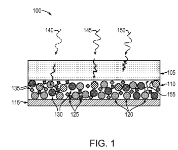
[0038] FIG. 1 depicts a cross-sectional view of a structure or device 100
that includes
a solar cell 105 and a spectral modification layer 110. In the illustrated
embodiment, the
spectral modification layer 110 is in optical communication with the back
(e.g., not light-
incident side) of solar cell 105. Optical communication can be achieved by
directly applying
spectral modification layer 110 directly to solar cell 105 without having
opaque intervening
layers (e.g., optically thick metal contacts). Reflective layer 115 is in
optical communication
with spectral modification layer 110.
[0039] Solar cell 105 can be a silicon solar cell (e.g., polycrystalline,
amorphous, etc.),
photovoltaic cell, dye-type solar cell, CdTe solar cell, or any other kind of
solar cell.
[0040] Spectral modification layer 110 can include various materials to
facilitate
spectral modification and/or scattering. In the illustrated embodiment,
spectral modification
layer 110 includes Raman shifting particles 120, adhesion/cohesion material
125, reflective
particles 130, and dopant material 135. Raman shifting particles 120 can
include diamond,
diamond powders, silicon, and/or TiO2 particles.
[0041] Adhesion/cohesion material 125 can be added to spectral
modification layer
110 to facilitate adhesion and/or cohesion of the materials in spectral
modification layer 110.
Adhesion/cohesion material 125 can be added to spectral modification layer 110
in particle
form or film form. The adhesion/cohesion material 125 can be highly reflective
or highly
transparent. For example, adhesion/cohesion material 125 can include aluminum,
silver
alloys, various low temperature melting glass, and/or plastics.
6
CA 02834149 2013-10-23
WO 2012/149026 PCT/US2012/035008
[0042] Reflective particles 130 can be added to spectral modification
layer 110 to
enhance scattering and/or electrical conductivity in the spectral modification
layer 110. In
some embodiments, reflective particles 130 will not substantially reduce the
performance
(e.g., scattering and/or Raman shifting performance) of the spectral
modification layer 110.
In some embodiments, reflective particles 130 can be highly reflective metals,
such as
aluminum, silver, and/or silver alloys. In some embodiments, reflective
particles can be
coated with well-known reflection enhancing coating to reduce parasitic
absorption losses.
Such coating can be applied to the outer and/or inner metal surface. Such
reflective
enhancing films may be prepared using existing technologies such as sputter
coating
[0043] Dopant material 135 can be added to spectral modification layer
110. Dopant
material 135 can be used to dope solar cell 105 by annealing (or heat
treatment), where
during annealing the dopant material 135 vaporizes and/or diffuses into the
material (e.g.,
silicon, silicon-germanium, and/or cadmium-telluride) of solar cell 105,
thereby increasing
the conductivity in the near surface regions of solar cell 105 to reduce
resistance at electrical
contacts. For example, when dopant material 135 includes aluminum particles
and is
incorporated in spectral modification layer 110, aluminum atoms may penetrate
the solar cell
105 during a subsequent anneal at ¨ 900C for several seconds.
[0044] Reflective layer 115 can be any reflective material. For example,
reflective
layer 115 can include aluminum, silver, or silver alloys.
[0045] While the illustrated embodiment shows structure or device 100
including
various components, it should be appreciated that the technology described
herein can be
implemented with a subset of those components. For example spectral
modification layer
110 can include a subset of Raman shifting particles 120, adhesion/cohesion
material 125,
reflective particles 130, and dopant material 135.
[0046] As an example of the operation of structure or device 100, red
light 140, green
light 145, and blue light 150 can be incident upon structure or device 100. In
the illustrated
embodiment, red light 140, green light 145, and blue light 150 are incident
upon solar cell
105. Green light 145 and blue light 150 are predominately absorbed by solar
cell 105. Red
light 140 can pass through solar cell 105 and into spectral modification layer
110. Spectral
modification layer 110 can scatter and wavelength shift (e.g., Raman shift)
red light 140 and
emit light 155 at a wavelength solar cell 105 can absorb (e.g., green or blue
light).
Reflective particles 130 can aid in conduction of electricity produced by
solar cell 105 and
facilitate longer travel paths for light (e.g., red light 140 and light 155)
in and/or passing
through spectral modification layer 110 and solar cell 105. It should be
appreciated that
7
CA 02834149 2013-10-23
WO 2012/149026 PCT/US2012/035008
spectral modification layer 110 can be configured to scatter and/or Raman
shift other
wavelengths of light depending on its composition and application.
[0047] FIG. 2 depicts a cross-sectional view of a structure or device 200
that includes
a solar cell 205 and a spectral modification layer 210. In the illustrated
embodiment, the
spectral modification layer 210 is in optical communication with the light-
incident side of
solar cell 205. Optical communication can be achieved by directly applying
spectral
modification layer 210 to solar cell 205 without having opaque intervening
layers (e.g.,
optically thick metal contacts). Reflective layer 215 is in optical
communication with the
back of solar cell 205.
[0048] Spectral modification layer 210 can include various materials to
facilitate
spectral modification and/or scattering. For example, spectral modification
layer 210 can
include Raman shifting particles 220, adhesion/cohesion material 225,
reflective particles
230, and dopant material 235, as described with respect to FIG. 1.
[0049] As an example of the operation of structure or device 200, red
light 240, green
light 245, and blue light 250 can be incident upon structure or device 200. In
the illustrated
embodiment, red light 240, green light 245, and blue light 250 are incident
upon spectral
modification layer 210. Green light 245 and blue light 250 can pass through
spectral
modification layer 210 and be absorbed by solar cell 205. Spectral
modification layer 210
can scatter and wavelength shift (e.g., Raman shift) red light 240 and emit
light 255 at a
wavelength solar cell 205 can absorb (e.g., green or blue light). It should be
appreciated that
spectral modification layer 210 can be configured to scatter and/or Raman
shift other
wavelengths of light depending on its composition and application.
[0050] FIG. 3 depicts a cross-sectional view of a structure or device 300
that includes
a transparent layer 305, solar cells 310, and a spectral modification layer
315. In the
illustrated embodiment, transparent layer 305 is separated from solar cells
310 and spectral
modification layer 315 by optical cavity 320. Transparent layer 305 can be in
optical
communication with solar cells 310 and spectral modification layer 315 via
optical cavity
320. Transparent layer 305 can be glass, a flexible material such as plastic,
or any other
material that is substantially transparent. In the illustrated example,
spectral modification
layer 315 can be used as an electrical rear contact for solar cells 310 and
serve as an electrical
conductor between solar cells 310.
[0051] In the illustrated embodiment, light (e.g., light 325) can be
absorbed directly by
solar cell 310 and/or scattered and Raman shifted by spectral modification
layer 315. Raman
shifted and/or scattered light (e.g., light 330) can be emitted from spectral
modification layer
8
CA 02834149 2013-10-23
WO 2012/149026 PCT/US2012/035008
315 for absorption by solar cell 310. Spectral modification layer 315 can be
made conductive
to aid collection from multiple solar or photovoltaic cells.
[0052] FIG. 4 depicts a cross-sectional view of a structure or device 400
that includes
a solar cell 410 and spectral modification layers 415. Spectral modification
layers 415 are in
optical communication with transparent regions 420. Spectral modification
layers 415 are
also in optical communication with reflective layers 425. Solar cell 410 is
separated from
spectral modification layers 415, transparent regions 420, and reflective
layers 425 by optical
cavity 430. In the illustrated embodiment, light 435 can enter transparent
regions 420
through an opening in spectral modification layers 415 and can be scattered by
and Raman
shifted by spectral modification layers 415 to produce scattered and Raman
shifted light 440.
Light 440 can be absorbed by solar cell 410. Transparent regions 420 can
include glass, air,
transparent plastic, etc. In some embodiments, structure or device 400 can be
prepared by
depositing spectral modification layers 415 onto two transparent regions 420
which are then
stacked as shown.
[0053] Performance of the described structures and/or devices can be
improved by
controlling the temperature of the structures or devices (or portions
thereof). For example,
solar cells and Raman scattering materials can have different ideal
temperatures of operation
for maximum solar cell performance and Raman shifting. To address this, in
some
applications, structure or device 300 and optical cavity 320 of FIG. 3 can be
maintained at a
different temperature than solar cell 310.
[0054] The functionality of spectral modification layers (e.g., spectral
modification
layer 110 of FIG. 1 or spectral modification layer 210 of FIG. 2) can be
improved (e.g., by
greater scattering, Raman shifting, or reflecting of light) by the inclusion
of additional
particles and/or additional layers applied to the above described devices
and/or structures.
For example, light scattering or Raman shifting composite particles can be
used to form
multifunction composite layers to facilitate spectral modification.
[0055] Light scattering and/or Raman shifting layers applied to either the
front face
(illuminated) and/or back (non-illuminated) face of a solar cell and/or in
optical
communication with a solar cell can be made more efficient by the inclusion of
additional
particles and/or by additional layers applied to the described light
scattering or Raman
shifting particles. For example, composite particles can be constructed from
Raman shifting
materials, light scattering materials, dopant materials, conductive materials,
and/or reflective
materials, or any combination thereof. A multifunction, composite spectral
modification
layer can be formed from composite particles and/or multiple particle types.
9
CA 02834149 2013-10-23
WO 2012/149026 PCT/US2012/035008
[0056] Distinct layer(s) and/or materials may be applied to all or part of
the particle
surface to create multifunction particles. The deposition of materials onto a
particle can
combine the various elements of the described spectral modification layers
(e.g., Raman
shifting materials, light scattering materials, dopant materials, conductive
materials, and/or
reflective materials) into a composite particle. Composite particles can have
a size ranging
from approximately a nanometer to microns for preferable diffuse reflection of
light and
Raman shift spectral modification rates.
[0057] Some embodiments of composite particles include a Raman shifting
material
(e.g., diamond or silicone), a scattering material (e.g., Ti02), and a
reflective material (e.g.,
silver, aluminum alloys, or other reflective materials), or any combination
thereof For
example, a composite particle can include diamond, TiO2 and silver. A
composite particle
can include diamond and Ti02. A composite particle can include diamond and
silver. A
composite particle can include TiO2 and silver.
[0058] Components of the described spectral modification layers can be in
film form
rather than particle form. Composite particles can be formed by coating
particles with other
materials. For example, metal can be coated onto Raman-scattering particles to
form a more
electrically conductive particle element. In some embodiments, a composite
particle can be
formed from a TiO2 particle partially coated with silver; a TiO2 particle
partially coated with
diamond and/or diamond-like film; or a TiO2 particle partially or fully coated
with diamond
and partially coated with silver. In some embodiments, a composite particle
can be formed
from a silver particle partially or fully coated with diamond and/or diamond-
like film; a silver
particle partially or fully coated with Ti02; or a silver particle partially
or fully coated with
diamond and/or diamond-like film and partially or fully coated with Ti02. In
some
embodiments, dopant materials can be added to the composite particles.
Existing coating
technologies such as sputtering coating may be used to prepare these films
and/or particles.
[0059] In some embodiments, composite particles consist of a low cost, non-
light
absorbing and/or light scattering particle (e.g., Ti02) at least partially
coated with diamond
film. The particles can be at least partially coated with a reflective metal
(e.g., aluminum)
that is designed (e.g., by alloying and/or by thickness) to melt or partially
melt at a
temperature that will bond the particles and other materials together (e.g.,
at 850 C). The
reflective material can, or other materials (e.g., boron) can be alloyed with
the reflective
metal to, have the capacity to dope (e.g., make more conductive) the near
surface region of
the solar cell material. For example, aluminum can be used as a dopant for
silicon solar sales.
CA 02834149 2013-10-23
WO 2012/149026 PCT/US2012/035008
[0060] FIG. 5A depicts a composite particle 500. As illustrated, composite
particle
500 includes a light scattering particle 505 (e.g., a Ti02, glass, or plastic
particle) partially
coated with a Raman-shifting material film 510 (e.g., diamond, diamond powder,
or any other
strongly Raman-shifting material), and partially coated with a reflective film
515 (e.g., a
metallic film, aluminum, etc.). The reflective film 515 can aid electrical
conduction and may
also serve as a semiconductor dopant source. In some embodiments, a reflection
enhancing
coating 520 can be applied to reflective film 515.
[0061] Composite Particle 500 can be used, for example, with and/or within
any of the
devices, structures, for films described herein. For example, composite
particle 500 can be
used in spectral modification layer 110 of FIG. 1 (e.g., as one or more of the
Raman shifting
particles 120, adhesion/cohesion material 125, reflective particles 130, or
dopant material
135) or in spectral modification layer 210 of FIG. 2 (e.g., as one or more of
the Raman
shifting particles 220, adhesion/cohesion material 225, reflective particles
230, or dopant
material 235).
[0062] FIG. 5B depicts a composite particle 550. As illustrated, composite
particle
550 includes a metal particle coated with shifting material film 555 (e.g.,
diamond, diamond
powder, or any other strongly Raman-shifting material). In some embodiments,
particle 550
can be partially coated with a reflective film 560 (e.g., a metallic film,
aluminum, etc.).
[0063] Composite particle 550 can be used, for example, with and/or within
any of the
devices, structures, for films described herein. For example, particle 550 can
be used in
spectral modification layer 110 of FIG. 1 (e.g., as one or more of the Raman
shifting particles
120, adhesion/cohesion material 125, reflective particles 130, or dopant
material 135) or in
spectral modification layer 210 of FIG. 2 (e.g., as one or more of the Raman
shifting particles
220, adhesion/cohesion material 225, reflective particles 230, or dopant
material 235). As
noted above, composite particles can be incorporated into and/or applied to
any of the
spectral modification layers described herein.
[0064] FIG. 6 depicts an arrangement 600 of composite particles 605A-605E.
Composite particles 605A-605E can be, for example, one or more of composite
particle 500,
as shown in FIG. 5A. Composite particles 605A-605D are illustrated in an
arrangement that
can facilitate conduction of electricity. In the illustrated embodiment,
particles 605A-605D
form a conductive path 610. Conductive path 610 can be formed, for example, by
the
reflective film 515 of composite particle 500 shown in FIG. 5A.
11
CA 02834149 2013-10-23
WO 2012/149026 PCT/US2012/035008
[0065] Arrangement 600 can also facilitate spectral modification. For
example, light
615 can be scattered and Raman-shifted by composite particles 605A-605E and
emitted as
light 620.
[0066] In some embodiments, a semiconductor dopant material 625 can be
deposited
onto composite particles 605A-605E.
[0067] FIG. 7 depicts a composite spectral modification layer 700.
Spectral
modification layer 700 can include Raman shifting particles 705, scattering
particles 710,
dopant material 715, and reflective adhesion/cohesion material 720. During
fabrication,
spectral modification layer 700 can be heated to melt and fuse reflective
adhesion/cohesion
material 720 to form paths of improved electrical conductivity (e.g., path
725) without
substantially blocking light traveling within and/or through spectral
modification layer 700.
[0068] Spectral modification layer 700 can be used, for example, with
and/or within
any of the devices, structures, or films described herein. For example,
spectral modification
layer 700 can be used as the spectral modification layer for any of the
embodiments described
herein.
Spectral Modification Layer Preparation
[0069] In some embodiments, the technology can involve films including
Raman
shifting particles. The Raman shifting particles can be silicon and/or diamond
particles. The
Raman shifting particles can be 2 nm in diameter or greater. In some
applications, the Raman
shifting particles can be approximately 50 nm in diameter. In some
embodiments, the Raman
shifting particles can be fully or partially coated with titanium oxide (Ti02)
or other
transparent and/or anti-reflective coating to reduce reflection by the Raman
shifting particles,
thereby promoting more Raman shifting within the film. In some embodiments,
the Raman-
shifting particles can be metal, silver, titanium oxide, glass, or other
material coated with a
Raman shifting material (e.g., diamond or silicon).
[0070] In some embodiments, the Raman shifting and other particles can be
embedded
in a matrix. The matrix can include a transparent or semi-transparent
material, such as a
matrix including glass particles. In some applications, the Raman shifting
particles can be
embedded in a light scattering matrix of particles to form a film. The matrix
can include
TiO2 particles. The film can include reflective particles, such as silver or
aluminum. In some
embodiments, the matrix can include particles of 2 nm in diameter or greater.
In some
applications, the matrix can include particles approximately 25-50 nm in
diameter.
12
CA 02834149 2013-10-23
WO 2012/149026 PCT/US2012/035008
[0071] The film can be applied to glass substrates or applied to the front
or back of
commercially-available silicon solar cells. In applications where the film is
applied to the
back of the solar cell, the rear contact of the cell can be removed. The films
can be applied to
the solar cell by preparing a slurry of the Raman shifting particles and light
scattering matrix
particles in a solution of water, acetic acid, and isopropanol, and spraying
the slurry onto
glass substrate or a solar cell. The films can be dried (e.g., annealed) at
approximately 500
Celsius for approximately 30 minutes and slowly cooled.
Experimental Results
[0072] Raman shifting can involve both an up conversion and a down
conversion
probability on each interaction with photons. The Raman process can be viewed
as a
diffusion process in photon energy as well as a spatial diffusion process,
where the spatial
diffusion process involves the physical travel and path length of a photon
scattering within
the particle materials of, for example, the films described herein.
[0073] The films described herein can facilitate long travel paths of
incident radiation
(e.g., light) within the films and solar cells. Applying diffusion theory to
the root-mean-
square (rms) displacement, d traveled by light yields Equation 1:
d 2 = Ni 2
rals
(1)
[0074] In
Equation 1, N is the number of path-altering scattering events and / is the
distance between scattering events. Since the total travel light path
displacement is given by
d=N1, d can in turn can be defined in terms of d as shown in Equation 2:
9
d
d -
(2)
[0075] Approximately kilometer-length travel paths for radiation can be
attained in
media having nano-spaced scattering structures (e.g., TiO2 particles) and
where d is a few
centimeters.
[0076] Experimental testing shows that the quantum efficiency at 1100 nm
of the as-
received commercial solar cells is in the range of approximately 10%. The
value of 1100 nm
is just beyond the band edge of the silicon solar cells used. The quantum
efficiency of a solar
13
CA 02834149 2013-10-23
WO 2012/149026 PCT/US2012/035008
cell using an aluminum-based rear contact can increase the quantum efficiency
to
approximately 15%. The 1100 nm quantum efficiency of solar cells in series
with Ti02-
silver diffuse rear reflector can increase to approximately 30% despite the
increased
resistance from being connected in series (series resistance can only decrease
the
performance below what it would be without this parasitic loss).
[0077] Titanium oxide and diamond/titanium oxide mixed-particle films of
various
thicknesses were prepared and applied to the rear of commercial silicon solar
cells (after
removal of the as-delivered rear contact paste). Similar films were also
deposited onto glass
slides using a standard hobby spray apparatus. To facilitate film spraying,
nanoparticles were
mixed with isopropanol and water. The films were then annealed at 500 C for
one hour and
slow-cooled. Film-coated glass slides were placed in front of the reference
silicon solar cell
(approximately 16% efficient under AM 1.5 illumination) and the quantum
efficiency
measured using a Newport Oriel quantum efficiency system with and without bias
light.
These same films were also placed in front of a standard germanium reference
photovoltaic
cell for visible and infrared ("IR") spectral transmission measurement. An
approximately 1.5
watt CW visible light laser was used for the bias light cases. These
experiments were also
performed with Titanium oxide and zirconium oxide/titanium oxide mixed-
particle films.
[0078] The Raman spectra of various embodiments of the technology (e.g.,
films)
were measured. The Raman shifting of 785 nm wavelength light by silicon and
diamond
nano-particles (e.g., particles approximately 50 nm in diameter) was measured
and compared
to Raman shifting in bulk crystals of the same materials. To quantify Raman
shifting
spectrum modification or management, glass substrates coated with the films
described
herein were placed in front of a reference silicon solar cell (the solar cell
having
approximately 16% efficiency under AM 1.5 illumination) and the quantum
efficiencies were
measured. Measurements were made with and without bias light. For comparison
to a flatter
spectral response photovoltaic cell and for long wavelength measurement a
commercial
germanium photovoltaic cell was also used.
[0079] The Raman shifts of bulk crystal and nanoscale (e.g., approximately
1 sum)
crystalline particles systems known to have large Raman shifts were measured
using a
Thermo Nicolet Almega dispersive Raman Spectrometer. FIG. 8 depicts the Raman
spectra
of crystalline and nanoscaled particle silicon as a function of light
intensity. In FIG. 8, the
response of silicon nanoparticles (e.g., 100 nm range) is shown. It was found
that the Raman
shift to the Anti-Stokes-to-Stokes ratio of the particle systems were greater
than their bulk
14
CA 02834149 2013-10-23
WO 2012/149026 PCT/US2012/035008
crystal counterparts. A relatively large Raman shift for particles, as
compared with bulk
crystal, was also found in visible-light-transparent particle systems. In all
cases the Anti-
Stokes-to-Stokes ratio increased with increasing probe and with bias light.
[0080] FIG. 8 is a graph showing the Raman spectra of bulk single crystal
silicon
compared to the Raman spectra of nano-scaled particle silicon. As seen in the
inset of FIG.
8, the d1 of a TiO2 film on a glass substrate is approximately 1 cm. Taking
the scattering
distance to be 25 nm, the TiO2 particle diameter, yields a light path length
of approximately 4
km.
[0081] As noted, the technology can utilize films including Raman shifting
particles
(e.g., silicon or diamond particles) in a matrix (e.g., TiO2 particles). In
some embodiments,
the Raman shifting particles and matrix are approximately transparent so as
not to absorb
light as it Raman and spatially scatters.
[0082] To test the ability of TiO2 particle matrices to spatially scatter
light with little
absorption, TiO2 films were applied in place of rear contacts on commercially-
available
silicon solar cells. The travel paths of light within the TiO2 films can
increase the probability
of the light being absorbed within the solar cell. The travel paths of light
within the TiO2
films can also increase the probability of Raman shifting events within the
films because as
light is scattered within these films, the light can encounter the Raman
shifting particles
multiple times.
[0083] A consideration for embodiments of the technology is the ratio of
Raman
shifting resulting in up-energy shifts, or anti-Stokes shifts, resulting in
shorter wavelength
light to Raman shifting resulting in down-energy shifts, Stokes shifts,
resulting in shorter
wavelength light. The down-energy shift probability is governed by phonon
emission
probabilities (or optical coupling constant) while the up-energy shift
probability is governed
by both the phonon absorption probability and the densities of pre-existing
phonons.
[0084] FIG. 8 illustrates that the ratio of Stokes to anti-Stokes shift
events in silicon is
a product of silicon crystal particle size, with the net Raman shift as well
as the anti-Stokes
shift to Stokes ratio increasing with decreasing particle size. Embodiments of
the technology
including diamond particles can behave in a similar manner. The anti-Stokes
shift probability
in both diamond and silicon particles can increase with increasing probe beam
intensity
and/or bias light.
CA 02834149 2013-10-23
WO 2012/149026 PCT/US2012/035008
[0085] For example, when the Raman spectra of diamond nano-particles were
compared to bulk diamond crystal using a 785 nm wavelength probe beam, the
anti-Stokes to
Stokes ratio was 0.012 for bulk diamond crystal and was 0.343 for diamond nano-
particles.
Accordingly, experimental results indicate that diamond nano-particles have a
greater anti-
Stokes response relative to the Stokes response than bulk diamond crystal.
When decreasing
the probe beam intensity, the anti-Stokes to Stokes ratio decreased to 0.062
for diamond
nano-particles whereas there was no significant change in the bulk diamond
crystal case.
[0086] Experimental results showed the net Raman shift and the anti-Stokes
to Stokes
ratio increased with decreasing particle size and with increasing probe beam
intensity (and
bias light) for both diamond and silicon, suggesting that the increased anti-
stokes response is
not due to particle heating. The experimental results are consistent with a
phonon transfer
mechanism in which phonons generated by Stokes shift events contribute to the
phonon
density in the exact wavelength ranges needed for subsequent anti-Stokes
events. Long
phonon lifetime is expected in small particles since phonon decay, in part,
relies upon longer
wavelength phonon decay products (Umklapp processes) that cannot exist in
small-sized
particles.
[0087] FIG. 9 depicts a comparison of a commercial solar cell with the as-
delivered
rear contact to a solar cell with a diffuse titanium oxide-based rear
reflector. As shown in
FIG. 9, a titanium oxide diffuse rear reflector can increase the quantum
efficiency at, for
example, wavelengths (X) of approximately 1,100nm by up to approximately 25%
as
compared to the aluminum pastes typically used on commercial crystal silicon
solar cells.
These rear scattering layers enable the use of flat, minimal-area, front
contacts that can
decrease the front surface recombination by more than a factor of two, when
compared with a
triangular light-scattering front surface structure.
[0088] The Raman shifts of the particle systems can produce both the
larger amplitude
shifts as well as the larger Anti-Stokes-to-Stokes ratios when compared to the
bulk crystal of
the same materials. The Anti-Stokes-to-Stokes shift increased with increasing
probe beam
intensity and it also increased with bias light illumination. The results are
consistent with a
phonon transfer mechanism, in which a phonon generated by a Stokes shift event
leaves
behind a long-enough-lived phonon to contribute to an anti-Stokes shift
(energy-increasing)
event. Careful analysis based upon a diffusion in energy predicted that more
than
approximately 30% of the Raman-shifted light will be towards higher energies
where the
photon could contribute to power generation.
16
CA 02834149 2013-10-23
WO 2012/149026 PCT/US2012/035008
[0089] Various films comprised of titanium oxide particles or titanium
particles, which
can facilitate Raman shifting, on glass substrates were placed in front of a
standard silicon
reference cell. FIG. 10 depicts the quantum efficiency of standard solar
cells. FIG. 10
illustrates that the back-scattering of the light reduced the overall quantum
efficiency of the
solar cell as film thickness increased. When the same films were placed in
front of the
germanium solar cells, the relatively featureless response of the germanium
photovoltaic cell
reveals a spectrally flat decrease in solar cell quantum efficiency,
indicating no spectral bias
in either film transmission or film light scattering.
[0090] Light transmission of the various films are spectrally flat ¨ the
quantum
efficiency ("QE") curves were normalized with respect to the response without
film cover.
The resultant plot is also shown in FIG. 10. FIG. 10 shows that, with strong
Raman-
scattering particles and with light bias, there is a distinct increase in the
quantum efficiency
("QE") near the band edge of silicon of 1100 nm.
[0091] Graph A of FIG. 10 shows the spectra response of a silicon solar
cell with
various diamond particle-based films on glass substrates placed on the front
(light incident
side) of the cell. The films of TiO2 and diamond particles on glass substrate
were placed in
front of a silicon solar cell to measure the quantum efficiency gains
resulting from Raman
shift-based spectral modification or management provided by the films. The
films reduced
the overall quantum efficiency of both cells with increasing film thickness
due to the amount
of light back-scattered away from the solar cell. The quantum efficiencies
shown in FIG. 10
were normalized (as indicated) with respect to the response without the
particle films. The
experimental results show that when used with films containing diamond nano-
particles, the
silicon solar cell has increased quantum efficiency near the band edge of
silicon and a relative
lack of response for the germanium phovoltaic cell (Graph B of FIG. 10).
[0092] Where the band-edge light makes many passes through the solar cell
and is
returned and re-scattered by the particles within the film, the Raman shift
probability can be
increased. The resulting anti-Stokes shifting of near band edge light
contributes to the
observed quantum efficiency for 975 nm wavelength light, as shown in Graph A
of FIG. 10.
The lack of similar gains in the germanium solar cell cases is consistent with
all light in the
measured spectral region being absorbed on its first pass through the solar
cell.
[0093] Spectral broadening can be quantified by considering an approximate
random
walk (e.g., approximate because up and down Raman shifts can have different
probabilities in
17
CA 02834149 2013-10-23
WO 2012/149026 PCT/US2012/035008
particle systems) in energy where the diffusion coefficient (D) for energy
hopping for Raman
shifting in silicon is provided by Equation 3:
, I c
D = IIAP = -(13 -1( AP )2 --- -(13 )(0..06)2
- -AO =
2 AI
(3)
In Equation 3, c is the speed of light, N is the refractive index, B is the
Raman shifting
probability per unit length, and 0.06 eV is the energy per Raman shift in
silicon particles (the
energy per Raman shift in diamond is larger).
[0094] Diffuse rear reflectors offer the advantage of scattering light to
sufficiently
large angles so as to increase probability of total internal reflection at the
front surface and,
therefore, much longer light path lengths within the solar cell absorber
layer, when compared
to a simple mirror-like rear reflector. To obtain a relatively large
scattering angle within a
high index solar cell (e.g., the refractive index of silicon is greater than
3.4), the diffuse rear
reflector should also have a large refractive index. For example, a sintered
rear reflector has
been found capable of increasing the long wavelength response by approximately
25%.
Interestingly, while diffuse rear reflectors increase performance, diffuse
front reflectors
decrease performance by approximately greater than 40%, mostly due to the
large amount of
light scattered and/or reflected out of the front of the solar cell (see,
e.g., FIG. 10).
[0095] The diffusion equation of energy hopping derived from that in
semiconductors
is Equation 4:
_________ -t ¨11 G = 0
n.
"0
(4)
In Equation 4, G is the incident flux of photon and a is the absorption
coefficient. The
lifetime of a photon is considered as a function of the absorption because the
photon is
assumed to live until it is absorbed. The boundary conditions are that no
photon is scattered
to zero energy and all photons with energy higher than the band gap are
absorbed. The
solution of Equation 4 is Equation 5:
18
CA 02834149 2013-10-23
WO 2012/149026
PCT/US2012/035008
i v
1_c d
n
I t L-s-.? ( i¨g)
1-- _________________________ lc 411.1 + (G A __ ,-- le
k." .1.-1: µ, ,_ t¨,f- ) 1, t I ' ie ;
- \ 111.--)d .' -li Ai ' '
e ¨ e e ¨ e
(5)
[0096] The collected photon current (e.g., photons having achieved an
energy
sufficient for absorption within the solar cell) is given by Equation 6:
(.:--
...,
¨ E
¨ ----
) ¨2
I = D VII .--- ( ¨G-, __________________________________________________ :11¨
I ¨ 4 i -,, --[ig COt,-1 ¨E.õ ) ¨ CSC ii( ,, i ¨1-: , A
-
:-,'---, ',,i 1., Ai '' v At
a , kid 4 -C
(6)
[0097] FIG. 11 is a graph showing the ratio of collected photon current to
the incident
photon flux as a function of the photon energy based on Raman-induced energy
diffusion of
light. FIG. 11 illustrates that the probability of Raman shifting must be
larger than the
probability of absorption. This is consistent with the result of FIG. 10,
where the increase in
response is seen in the near-band-edge region of silicon where absorption is
low and the
energy-distance to collection is small because as the ratio of Raman shifting
to absorption
probability decreases, the ability to collect low energy photon decreases.
19