Note: Descriptions are shown in the official language in which they were submitted.
CA 02834891 2013-10-31
WO 2012/166562
PCT/US2012/039487
TITLE OF THE INVENTION
GRAPHENE MAGNETIC TUNNEL JUNCTION SPIN
FILTERS AND METHODS OF MAKING
Priority Data and Incorporation by Reference
[0001] This application claims benefit of priority to U.S. Provisional Patent
Application No. 61/490,650 filed May 27, 2011 which is incorporated by
reference in its
entirety.
FIELD OF THE INVENTION
[0002] The present invention relates to methods of forming a few molecule
thick (1-3
or 4 monolayer) graphene layer on a ferromagnetic layer, at temperatures and
conditions
consistent with integration with silicon¨based complementary metal oxide
semiconductors
(Si CMOS). Specifically, this invention permits for the first time the
manufacture of magnetic
tunnel junction spin filters and related devices based on graphene on Si CMOS
devices at
temperatures and conditions consistent with those preexisting structures.
BACKGROUND OF THE INVENTION
[0003] The increasing demand for high density magnetic recording and playback,
and
requirements for non-volatile memory, have focused attention on magnetic
tunnel junctions,
and the devices that can be prepared therefrom, such as MRAMs and the like. To
date, the
most advanced magnetic tunnel junctions are principally made of ferromagnetic
sandwiches
of thin films of aluminum oxide electron tunneling barriers between a metal
which is
typically iron, cobalt or nickel. Recently, crystalline magnesium oxide has
been proposed as
the barrier layer. Different materials are selected to improve the observed
tunnel magnetic
resistance values. Even with thirty (30) years of intensive investigation, the
highest TMR
values for the Fe/MgO/Fe are about Two Hundred Forty Percent (240%).
1
SUBSTITUTE SHEET (RULE 26)
CA 02834891 2013-10-31
WO 2012/166562
PCT/US2012/039487
[0004] Graphene offers decided advantages for the tunnel barrier in a magnetic
tunnel junction. Indeed, magnetic tunnel junctions (FIG.1) composed of FM/few-
layer
graphene/FM stacks (FM = ferromagnet, i.e., Co, Ni) have been proposed [1] as
"perfect
spin" filters. The ability to form such stacks on, e.g., Cu interconnect lines
would allow
direct integration with Si CMOS, leading to broad new capabilities in non-
volatile memory,
spin-logic, and defect-tolerant, adaptive computing [2-5]. This in turn
requires the ability to
form multiple graphene layers on Co substrates, and to do so at temperatures
below ¨ 700 K,
the thermal stability limit of low-k dielectric materials currently employed
in advanced Si
CMOS devices.
[0005] Graphene growth by CVD or PVD on Co surfaces is well-reported, but is
usually carried out at higher temperatures (> 1000 K). Ago, et al, [9] reports
the growth of
ordered multilayer graphene films on Co(111)/alumina films by CVD (CH4 and H2)
at > 1150
K. Varykhalov and Rader [12] report the growth of epitaxial graphene on
Co(0001)/W(110)
by CVD of propylene at ¨ 730 K. Graphene films non-uniform in thickness have
been grown
on polycrystalline Co films by CVD (ethylene) at 1073 K [13]. To date, there
has not been a
satisfactory report of formation of few-layer graphene films followed by
annealing to give
operative devices at temperatures below 700 K.
[0006] Thus, in a typical magnetoresistive random access memory, an array of
parallel first conductive lines is presented on a horizontal plane, and an
array of parallel
second conductive lines on a second horizontal plane is disposed above the
first array in a
direction perpendicular to the first array of conductive lines. See, for
example, U.S. Patent
No. 7,985,579, the disclosure of which pertaining to the formation of MRAMs is
incorporated herein-by-reference. The MTJ element is disposed between the two
arrays at
each crossover point. This requires a technology that permits formation of the
stack, and
annealing to operative conditions, at Si CMOS compatible temperatures to be
integrated in
2
SUBSTITUTE SHEET (RULE 26)
CA 02834891 2013-10-31
WO 2012/166562
PCT/US2012/039487
today's dominant electronic and photonic technologies, particularly
communications and
computing equipment.
SUMMARY OF THE INVENTION
[0007] Deposition of ferromagnetic materials such as cobalt and nickel on
copper
interconnects on Si CMOS devices has been well established. Applicants now
demonstrate
that few layer graphene films can be formed directly on cobalt or nickel
layers at
temperatures and conditions compatible with the requirements of Si CMOS
fabrication, to
provide MTJ spin filters and related devices, for development of various types
of non-volatile
memory, by forming a FM layer atop an interconnect (for instance, of copper)
and then
annealing the deposited metal (preferably cobalt, nickel) to segregate carbon
in the metal
layer formed. Annealing at ultra-high vacuum of lower than about 10"7 toff
yields a few-layer
thick graphene layer on the metal, which can be overlaid with a sandwiching
film of metal,
all at temperatures and conditions consistent with silicon CMOS fabrication
and operation.
The resulting sandwich or stack provides an MTJ of superior properties.
BRIEF DESCRIPTION OF THE DRAWINGS
[0008] The accompanying drawings, which are incorporated herein and constitute
part of this specification, illustrate exemplary embodiments of the invention,
and, together
with the general description given above and the detailed description given
below, serve to
explain the features of the invention.
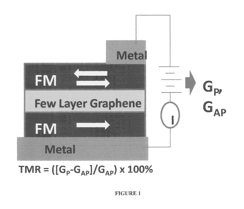
[0009] FIG. 1 is a schematic of an MTJ device of the invention. Orientation of
the
two FM anodes parallel (P) or antiparallel (AP) results in corresponding
tunneling
conductances Gp,GAp. Definition of TMR (tunneling magnetoresistance) in terms
of Gp, GAP
is also shown.
3
SUBSTITUTE SHEET (RULE 26)
CA 02834891 2013-10-31
WO 2012/166562
PCT/US2012/039487
100101 FIG. 2 reflects evolution of C(KVV) Auger lineshape upon annealing a
cobalt
film of ¨ 40 A deposited on A1203(0001). Average graphene layer thickness
derived from
Auger intensities is ¨ 3.5 monolayers. Annealing conditions: 600 K in UHV, 70
min.
[0011] FIG. 3 reflects corresponding LEED image data showing a graphene
lattice in
an R30 position relative to Co. The relatively narrow nature of the graphene
spots indicates a
high degree of azimuthal ordering of the graphene layers.
[0012] FIG. 4 presents graphically predicted Gp and GAp values for a FM/few
layer
graphene/FM MTJ as a function of the number of graphene layers, from ref. [1].
[0013] FIG. 5 is a LEED image of few-layer graphene on ordered Co film grown
by
CVD (CH4 + H2) at ¨ 1200 K. Note the streaky nature of graphene spots
corresponding to the
graphene lattice, indicative of azimuthal randomization. This figure is a
reference figure
taken from ref. [9].
DETAILED DESCRIPTION OF THE INVENTION
Procedures and Results
[0014] The FM/few layer graphene/FM stack based MTJ of the invention was made
by first using electron beam evaporation to deposit ¨ 40 A of (disordered)
cobalt on a A1203
(0001) substrate, at a background pressure of ¨ 1 x 10⁻⁸TOIT, resulting in
some carbon being
dissolved in the cobalt film. Annealing of the film to ¨ 600 K in UHV results
in the
segregation of dissolved carbon to the surface of the cobalt film as it orders
to form a
Co(111) film with carbon overlayer.
[0015] Auger C(KVV) Auger data (FIG. 2) shows that the thickness of the carbon
overlayer grows to an average thickness of ¨ 3.5 monolayers during the
annealing process,
while transforming from sp3 to sp2 carbon chemical bonding¨the formation of
few layer
graphene.
4
SUBSTITUTE SHEET (RULE 26)
CA 02834891 2013-10-31
WO 2012/166562
PCT/US2012/039487
[0016] Corresponding LEED data (FIG. 3) obtained from the carbon segregation
event demonstrate that the graphene layers are highly ordered, displaying well-
defined
diffraction spots at 300 relative to the Co diffraction spots. The Auger data
(FIG. 2) also
show an absence of carbide formation, indicating a chemically abrupt Co/carbon
interface
which does not disrupt the graphene n network, and which should not depolarize
the Co
surface layer via oxidation [6]. Indeed, the presence of a uniform graphene
layer has been
demonstrated to inhibit oxidation of transition metal surfaces even upon
ambient exposure [7-
10] and can be an important factor in device processing under industrial
conditions.
[0017] Following annealing, a similar cobalt layer is deposited over the
graphene to a
thickness of approximately forty (40) angstroms, giving a high performance MTJ
which is
readily incorporated in an MRAM or other non-volatile memory device, during
fabrication.
Thus, at desired locations (crossover points) in the underlying array of
contact lines, the
cobalt or nickel or similar layer (other metals, such as iron, gadolinium
(Gd), and neodymium
(Nd) are potentially applicable, but less favored) is deposited by electron
beam evaporation,
and then annealed below 700 K. Following formation of the graphene
intermediate layer, a
top or "cap" of cobalt or nickel is applied, and the overlying array of
conductive lines is
formed ¨ forming the MRAM array as part of initial fabrication.
Impact and Potential Benefits
[0018] The completion of a Co/3.5 monolayer graphene/Co junction via the
deposition of a Co layer on few layer graphene, as per FIG. 1, would have a
predicted [1]
spin filtering effect of ¨ 75-80% (FIG. 1). Tunneling magnetoresistance (TMR)
is usually
defined [6] as:
(1) TMR = (Gp - GAp)/GAp
This predicted value, as set forth in Karpan et al, is set artificially low.
In the calculations set
forth in Figure 4, the denominator is G(parano instead of G(antiparallel) as
normally done. This was
SUBSTITUTE SHEET (RULE 26)
CA 02834891 2013-10-31
WO 2012/166562
PCT/US2012/039487
done since, in graphene, G(antiparallel) becomes vanishingly small.
Traditional calculations give
TMR values well in excess of one thousand percent (1000%) but are difficult to
calculate
with certainty.
[0019] The predicted [1]TMR values for a Co/3.5 monolayer graphene/Co
structure
are therefore ¨ 103. Further increases in the number of graphene layers, by
enhancing
segregation of carbon, longer annealing times, etc. could increase the TMR
value to ¨ 1012.
In contrast, the best reported existing TMR value, obtained for a MTJ based on
a Fe
alloy/Mg(100)/Fe(100) device[11] is only ¨ 240%. The high TMR values for the
Co/graphene/Co device (FIG. 1) allow much larger arrays, smaller devices, and
give an
on/off ratio approaching or exceeding that of existing Si CMOS devices.
Other Potential Benefits Include:
[0020] Co(111) films can be formed at room temperature on Cu(111) without Cu-
Co
alloying. Device formation at temperatures below ¨ 770 K inhibits interfacial
diffusion, and
a Co fcc4hcp phase transition. This allows for the formation of Co or Ni films
on Cu
without a diffusion barrier, greatly simplifying processing.
[0021] The process set forth above is self-developing and self-aligning:
graphene
films grow only where Co has been deposited, thus eliminating the need for
graphene
patterning to form device structures.
[0022] FM/graphene/FM MTJ's are predicted [1] to be highly tolerant of
disorder to
interfacial structure. Accordingly it is possible to form MTJ structures of
this type on
polycrystalline Cu interconnect lines using polycrystalline Co, thus allowing
such devices to
be made directly with current processing methods.
Comparison with Prior Art
[0023] The relative ordering of multilayer graphene films from the above-
described
process appears high (FIG. 3). In contrast, films grown by AgO, et al. [9]
appear to be
6
SUBSTITUTE SHEET (RULE 26)
CA 02834891 2013-10-31
WO 2012/166562
PCT/US2012/039487
azimuthally disordered (FIG. 5) as evidenced by the appearance of streaks,
rather than spots,
corresponding to the graphene lattice. Loss of optimum MTJ performance
parameters aside,
the processing temperatures involved for these and other graphene films formed
by CVD (>
750 K) pose significant problems for integration with Si CMOS at the
interconnect or
packaging levels. Applicant's invention permits the direct fabrication of
MTJ's in Si CMOS
devices using conventional technology, operating at high performance at
ambient conditions.
References
[0024] [1] V.M. Karpan, P.A. Khomyakov, A.A. Starikov, G. Giovarmetti, M.
Zwierzycki, M. Talarmana, G. Brocks, J. van den Brink, P.J. Kelly, Phys. Rev.
B. 78 (2008)
195419.
[0025] [2] R. Richter, L. Bar, J. Wecker, G. Reikss, Appl. Phys. Lett. 80
(2002)
1291.
[0026] [3] R. Richter, H. Boeve, L. Bar, J. Bangert, G. Rupp, G. Reiss, J.
Wecker,
Solid State Electronics 46 (2002) 639.
[0027] [4] J.R. Heath, P.J. Kuekes, G.S. Snider, R.S. Williams, Science 280
(1998)
1716.
[0028] [5] W.C. Black Jr. and B. Das, J. Appl. Phys. 87 (2000) 6674.
[0029] [6] J.P. Velev, P.A. Dowben, E.Y. Tsymbal, S.J. Jenkins, A.N. Caruso,
Surf.
Sci. Rept. 63 (2008) 400.
[0030] [7] Y.S. Dedkov, M. Fonin, U. Rudiger, C. Laubschat, Phys. Rev. Lett.
100
(2008) 107602.
[0031] [8] M. Weser, Y. Rehder, K. Horn, M. Sicot, M. Fonin, A.B.
Preobrajenski,
E.N. Voloshina, E. Goering, Y.S. Dedkov, Appl.Phys. Lett. 96 (2010) 012504.
[0032] [9] H. Ago, Y. Ito, N. Mizuta, K. Yoshida, B. Hu, C.M. Orofeo, M.
Tsuji, K.
Ikeda, S. Mizuno, ACS Nano 4 (2010) 7407.
7
SUBSTITUTE SHEET (RULE 26)
CA 02834891 2013-10-31
WO 2012/166562
PCT/US2012/039487
[0033] [10] L. Kong, C. Bjelkevig, S. Gaddam, M. Zhou, Y.H. Lee, G.H. Han,
H.K.
Jeong, N. Wu, Z. Zhang, J. Xiao, P.A. Dowben, J.A. Kelber, J. Phys. Chem. C.
114 (2010)
21618.
[0034] [11] F. Bone11, S. Andrieu, F. Bertran, P. Lefever, A.T. Ibrahimi, E.
Snoeck,
C. Tiusan, F. Montaigne, IEEE Trans. Mag. 45 (2009) 3467.
[0035] [12] A. Varykhalov and O. Rader, Phys. Rev. B. 80 (2009) 035437.
[0036] While the current invention has been disclosed with references to
certain
embodiments, numerous modification, alterations, and changes to the described
embodiments
are possible without departing from the sphere and scope of the present
invention, as defined
in the appended claims. Accordingly, it is intended that the present invention
not be limited
to the described embodiments, but that it has the full scope defmed by the
language of the
following claims, and equivalents thereof.
8
SUBSTITUTE SHEET (RULE 26)