Note: Descriptions are shown in the official language in which they were submitted.
1
Device for signature adaptation and object provided with such a device
TECHNICAL FIELD
The present invention pertains to a device for signature adaptation. The
present
invention also pertains to an object such as a vehicle.
BACKGROUND
Military vehicles/crafts are subjected to threats, e.g. in a situation of war,
constituting targets for attack from land, air and sea. It is therefore
desired that the
vehicle is as difficult as possible to detect and identify. For this purpose
military
vehicles are often camouflaged to the background such that they are difficult
to
detect and identify with the bare eye. Further, they are hard to detect in
darkness
with different types of image intensifiers. A problem is that attacking crafts
such as
combat vehicles and aircrafts often are equipped with a combination of one or
more active and/or passive sensor systems comprising radar and electro-
optic/infrared (E0/IR) sensors wherein the vehicles/crafts become relatively
easy
targets to detect, classify and indentify. Users of such sensor systems search
for a
certain type of thermal/reflecting contour normally not occurring in nature,
usually
different edge geometries, and/or large evenly heated surfaces and/or even
reflecting surfaces.
In order to protect against such systems different types of techniques are at
present used in the area of signature adaptation. Signature adaptation
techniques
comprises constructional actions and are often combined with advanced material
techniques in order to provide a specific emitting and/or reflecting surface
of the
vehicles/crafts in all wave length areas wherein such sensor systems operate.
CA 2835160 2018-05-23
CA 02835160 2013-11-05
WO 2012/169958
PCT/SE2012/050601
2
US2010/0112316 Al describe a visual camouflage system that provides at
least thermal suppression or radar suppression. The system comprises a
vinyl layer having a camouflage pattern on a front surface of the vinyl layer.
The camouflage pattern comprises a location specific camouflage pattern. A
laminate layer is attached over the front surface of the vinyl layer to
provide a
protection over the camouflage pattern and a reinforcement of the vinyl layer.
One or more nano material is applied to at least one of the vinyl layer, the
camouflage pattern or the laminate to provide at least one of a thermal or
radar suppression. This solution only enables static signature adaptation.
WO/2010/093323 Al describe a device for thermal adaptation, comprising at
least one surface element arranged to assume a determined thermal
distribution, said surface element comprising a first heat conducting layer, a
second heat conducting layer, said first and second heat conducting layers
being mutually thermally isolated by means of an intermediate insulation
layer, wherein at least one thermoelectric element is arranged to generate a
predetermined temperature gradient to a portion of said first layer. The
invention also relates to an object such as a craft. This solution only
enables
thermal signature adaptation.
OBEJCTIVE OF THE INVENTION
An object of the present invention is to provide a device for signature
adaptation that handles both radar and thermal signature adaptation.
An additional object of the present invention is to provide a device for
thermal
and radar signature adaptation which facilitates thermal and radar
camouflage with desired thermal and radar cross section (RCS).
An additional object of the present invention is to provide a device for
thermal
and radar camouflage which facilitates automatic thermal adaptation of
surrounding and passive radar adaptation of surrounding and which
facilitates providing a un-even thermal structure.
3
Another object of the present invention is to provide a device for thermally
and in
terms of radar imitating e.g. other vehicles/crafts in order to provide
thermal and
radar identification of own troops or to facilitate thermal and radar
infiltration in or
around e.g. enemy troops during suitable circumstances.
SUMMARY OF THE INVENTION
These and other objects, apparent from the following description, are achieved
by
a device, a method for signature adaptation and an object, which is of the
type
stated by way of introduction.
According to the invention the objects are achieved by a device for signature
adaptation, comprising at least one surface element arranged to assume a
determined thermal distribution, wherein the surface element comprises at
least
one thermoelectric element for generating at least one predetermined
temperature
gradient to a portion of a first heat conducting layer of the at least one
surface
element, wherein the at least one surface element comprises at least one radar
suppressing element, wherein the at least one radar suppressing element is
configured to suppress reflections of incident radio waves, and comprises one
or
more radar absorbing materials or surface layers, wherein the radar
suppressing
element is arranged interiorly relative to the first heat conducting layer and
wherein
the first heat conducting layer is provided with a frequency selective surface
structure so that incident radio waves are filtered and passed through the
first heat
conducting layer whereby incident radio waves are absorbed by the radar
suppressing element.
Hereby is facilitated an efficient thermal and adaptation and radar
suppression. A
certain application of the present invention is thermal and radar signature
adaptation for camouflaging of e.g. military vehicles, wherein said at least
one
temperature generating element facilitates efficient thermal adaptation and
wherein
CA 2835160 2018-05-23
3a
said at least one radar suppressing element facilitates adaptation of radar
signature, so that dynamic thermal signature adaptation with maintained low
observability within the radar area may be kept during motion of the vehicle.
CA 2835160 2018-05-23
CA 02835160 2013-11-05
WO 2012/169958
PCT/SE2012/050601
4
According to an embodiment of the device said at least one temperature
generating element is thermally arranged to a sub surface area of said
portion of said at least one surface element for generation of said at least
one
temperature gradient to said portion.
According to an embodiment of the device said portion constitutes at least
one outer layer of said at least one surface element.
According to an embodiment of the device wherein said at least one outer
layer is arranged to provide a frequency selective sub surface area, wherein
said frequency selective sub surface area is arranged to pass through radio
waves within a predetermined frequency range and wherein said frequency
selective sub surface area have heat conducting properties. By providing an
outer layer that is frequency selective and that has heat conducting
properties it is facilitated to quickly reach a desired temperature of said at
least one outer layer and further that incident radio waves within a frequency
range typically associated to radar systems is transmitted through said outer
layer in order to subsequently be absorbed by said at least one radar
suppressing element. Further is facilitated to provide an outer layer that is
robust and durable such as for example a metallic outer layer.
According to an embodiment of the device said frequency selective sub
surface is arranged to surround said sub surface area of said portion.
According to an embodiment of the device said frequency selective sub
surface and said sub surface area to which said at least one temperature
generating element is thermally applied, are mutually arranged so that the
permeability for radio waves substantially do not impair the heat
conductibility
of said portion.
According to an embodiment of the device said at least one surface element
comprises at least one display surface having thermal permeability and
arranged to radiate at least one predetermined spectrum. Hereby is
facilitated also visual signature adaptation apart from radar signature
CA 02835160 2013-11-05
WO 2012/169958
PCT/SE2012/050601
adaptation and thermal signature adaptation. Thereby is facilitated also
radar, thermal and visual adaptation for camouflage of e.g. military vehicles,
wherein the combination of said radar suppressing element said at least one
display surface and said at least one temperature generating element
5 facilitates efficient dynamic adaptation of visual signature (colour,
pattern)
and thermal signature with maintained low radar cross section occurring for
stationary vehicles and during motion of the vehicle. By providing a display
surface having a thermal permeability, within which said predetermined
temperature gradient falls, is further facilitated a de-coupled solution that
allows to individually adapt thermal and visual signature independently of
each other.
According to an embodiment of the device said at least one display surface is
arranged to permit said at least one predetermined temperature gradient to
be maintained of said at least one surface element. Hereby is facilitated
efficient thermal signature adaptation together with visual signature
adaptation without affecting each other.
According to an embodiment of the device said at least one display surface is
of emitting type. This provide a cost efficient device.
According to an embodiment of the device said at least one display surface is
of reflecting type. Using a display surface of reflecting type facilitates
reproducing a more lifelike image of the surrounding environment since
display surfaces of reflective type uses natural incident light to radiate
said at
least one spectrum instead of using one or more active light sources in order
to radiate said at least one spectrum.
According to an embodiment of the device said at least one display surface is
arranged to radiate at least one predetermined spectrum comprising at least
one component within the visual area and at least one component within the
infrared area. By radiating one or more spectrum comprising components
falling within the infrared area and one or more components falling within the
CA 02835160 2013-11-05
WO 2012/169958
PCT/SE2012/050601
6
visual area it is facilitated using the components falling within the infrared
area to control also the thermal signature apart from the visual signature.
This means that thermal signature adaptation can be achieved quicker as
compared to only using the temperature generating element.
According to an embodiment of the device said at least one display surface is
arranged to radiate at least one predetermined spectrum in a plurality of
directions, wherein said at least one predetermined spectrum is directionally
dependent. By radiating at least one predetermined spectrum in a plurality of
directions it is facilitated to correctly re-creating perspectives of visual
.. background objects by reproducing different spectrums (pattern, colour) in
different direction whereby a viewer independently of relative position views
a
correct perspective of said visual background object. According to an
embodiment of the device said at least one display surface comprises a
plurality of display sub surfaces, wherein said display sub surfaces are
arranged to radiate at least one predetermined spectrum in at least one
predetermined direction, wherein said at least one predetermined direction
for each display sub surface is individually displaced relative an orthogonal
axis of said display surface. By providing a plurality of display sub-surfaces
it
is facilitated to reproduce a plurality of directionally dependent spectrums
using a single display surface since each display sub surface is individually
controllable.
According to an embodiment of the device said at least one display surface
comprises an obstructing layer arranged to obstruct incident light and a
underlying curved reflecting layer arranged to reflect incident light. By
.. providing an obstructing layer it is facilitated to reproduce a plurality
of
directionally dependent spectrums using a single display surface in a cost
efficient fashion. As an example said obstructing layer may be formed by thin
film.
Furthermore it is facilitated that spectrums adapted to be reproduced in a
.. certain angle or angular range are not visible in viewing angles falling
outside
CA 02835160 2013-11-05
WO 2012/169958
PCT/SE2012/050601
7
of said certain angle of angular range, as a result of using said obstructing
layer.
According to an embodiment of the device said the device comprises at least
one additional element arranged to provide armour. By providing at least one
additional element arranged to provide armour it is facilitated apart from
increasing the robustness to provide a device forming a modular armour
system wherein individual forfeited surface elements of crafts easily can and
cost efficiently can be replaced.
According to an embodiment the device further comprises at least one
framework or support structure, wherein said at least one framework or
support structure is arranged to supply current and control
signals/communication. As a result of the framework per se being arranged
to deliver current, the number of cables may be reduced.
According to an embodiment the device comprises a first heat conducting
layer, a second heat conducting layer, said first and second heat conducting
layer being mutually thermally isolated by means of an intermediate
insulation layer, wherein at least one thermoelectric element is arranged to
generate a predetermined temperature gradient to a portion of said first layer
and wherein said first layer and said second layer have anisotropic heat
conduction such that heat conduction mainly occurs in the main direction of
propagation of the respective layer. By means of the anisotropic layers a
quick and efficient transport of heat is facilitated and consequently quick
and
efficient adaptation. By increasing ratio between heat conduction in the main
direction of propagation of the layer and heat conduction crosswise to the
layer it is facilitated to arrange the thermoelectric elements at a larger
distance from each other in a device with e.g. several interconnected surface
elements, which results in a cost efficient composition of surface elements.
By increasing the ratio between the heat conductibility along the layer and
the heat conductibility crosswise to the layer the layers may be made thinner
and still achieve the same efficiency, alternatively make the layer and thus
CA 02835160 2013-11-05
WO 2012/169958
PCT/SE2012/050601
8
the surface element quicker. If the layers become thinner with retained
efficiency, they also become cheaper and lighter. Furthermore it is
facilitated
a more even distribution of heat in layers arranged directly underneath the
display surface which heavily reduces the possibility that potential hot-spots
of underlying layers affects the ability of said display surface to correctly
reproduce spectrums.
According to an embodiment of the device further comprises an intermediate
heat conducting element arranged in the insulation layer between the
thermoelectric element and the second heat conducting layer, and has
anisotropic heat conduction such that heat conduction mainly occurs
crosswise to the main direction of propagation of the second heat conducting
layer.
According to an embodiment of the device the surface element has a
hexagonal shape. This facilitates simple and general adaption and assembly
during composition of surface elements to a module system. Further an even
temperature may be generated on the entire hexagonal surface, wherein
local temperature differences which may occur in corners of e.g. a squarely
shaped module element are avoided.
According to an embodiment the device further comprises a visual sensing
means arranged to sense the surrounding visual background e.g. visual
structure. This provides information for adaptation of radiated at least one
spectrum from said at least one display surface of surface elements. A visual
sensing means such as a video camera provides an almost perfect
adaptation of the background, wherein the visual structure of a background
(colour, pattern) may be reproduced representable on e.g. a vehicle arranged
with several interconnected surface elements.
According to an embodiment of the device said device further comprises
thermal sensing means arranged to sense surrounding temperature, such as
for example thermal background. This provides information for adaptation
CA 02835160 2013-11-05
WO 2012/169958
PCT/SE2012/050601
9
surface temperature of surface elements. A thermal sensing means such as
an IR-camera provides an almost perfect adaptation of the thermal structure
of the background, temperature variations may be reproduced representable
on e.g. a vehicle arranged with several interconnected surface elements. The
.. resolution of the IR-camera may be arranged to correspond to the resolution
being representable by the interconnected surface elements, i.e. that each
surface element corresponds to a number of grouped camera pixels. Hereby
a very good representation of the background temperature is achieved such
that e.g. heating of the sun, spots of snow, pools of water, different
properties
of emission etc. of the background often having another temperature than the
air may be represented correctly. This efficiently counteracts that clear
contours and evenly heated surfaces are created such that when the device
is arranged on a vehicle a very good thermal camouflaging of the vehicle is
facilitated.
According to an embodiment of the device the surface element has a
thickness in the range of 5-60 mm, preferably 10-25 mm. This facilitates a
light and efficient device.
BRIEF DESCRIPTION OF THE DRAWINGS
A better understanding of the present invention will be had upon the
reference to the following detailed description when read in conjunction with
the accompanying drawings, wherein like reference characters refer to like
parts throughout the several views, and in which:
Fig. la schematically illustrates an exploded three dimensional view of
different layers of a part of the device according to an embodiment of the
.. present invention;
Fig. lb schematically illustrates an exploded side view of different layers of
a
part of the device in fig la;
CA 02835160 2013-11-05
WO 2012/169958
PCT/SE2012/050601
Fig. 2 schematically illustrates a device for signature adaptation according
to
an embodiment of the present invention;
Fig. 3a schematically illustrates the device for signature adaptation arranged
on an object such as a vehicle, according to an embodiment of the present
5 invention;
Fig. 3b schematically illustrates an object such as a vehicle where the
thermal and/or visual structure of the background using the device according
to the present invention is reproduced on two parts of the vehicle;
Fig. 4a schematically illustrates an exploded three dimensional view of
10 different layers of a part of the device according to an embodiment of
the
present invention;
Fig. 4b schematically illustrates flows in a device according to an
embodiment of the present invention;
Fig. 5 schematically illustrates an exploded side view of a part of the device
for thermal adaptation according to an embodiment of the present invention;
Fig. 6a schematically illustrates an exploded three dimensional view of
different layers of a part of the device according to an embodiment of the
present invention;
Fig. 6b schematically illustrates an exploded side view of different layer of
a
part of the device in fig 6a;
Fig. 7a schematically illustrates a side view a type of display layer of a
part of
the device according to an embodiment of the present invention;
Fig. 7b schematically illustrates a side view a type of display layer of a
part of
the device according to an embodiment of the present invention;
Fig. 7c schematically illustrates a plan view of a part of a display layer of
a
part of the device according to an embodiment of the present invention;
CA 02835160 2013-11-05
WO 2012/169958
PCT/SE2012/050601
11
Fig. 7d schematically illustrates a side view of a display layer according to
an
embodiment of the present invention;
Fig. 7e schematically illustrates a plan view of a display layer according to
an
embodiment of the present invention;
Fig. 8a schematically illustrates a plan view of different layers of a part of
the
device according to an embodiment of the present invention;
Fig. 8b schematically illustrates a plan view of flows of different layers of
a
part of the device according to an embodiment of the present invention;
Fig. 9 schematically illustrates an exploded three dimensional view of
different layers of a part of the device according to an embodiment of the
present invention;
Fig. 10 schematically illustrates a plan view of a device according to an
embodiment of the present invention;
Fig. 11 schematically illustrates a device for signature adaptation according
to an embodiment of the present invention;
Fig. 12a schematically illustrates a plan view of a module system comprising
elements for recreating thermal background or similar;
Fig. 12b schematically illustrates an enlarged part of the module system in
fig. 12a;
Fig. 12c schematically illustrates an enlarged part of the part in fig. 12b,
Fig. 12d schematically illustrates a plan view of a module system comprising
elements for recreating thermal and/or visual background or similar according
to an embodiment of the present invention;
Fig. 12e schematically illustrates a side view of the module system in fig.
12d;
CA 02835160 2013-11-05
WO 2012/169958
PCT/SE2012/050601
12
Fig. 12f schematically illustrates a side view of a module system comprising
elements for recreating thermal and/or visual background or similar according
to an embodiment of the present invention;
Fig. 12g schematically illustrates an exploded three dimensional view the
module system in fig. 12f,
Fig. 13 schematically illustrates an object such as a vehicle subjected to a
threat in a direction of threat, the background of the thermal and/or visual
structure being recreated on the side of the vehicle facing in the direction
of
threat;
Fig. 14 schematically illustrating different potential directions of threat
for an
object such as a vehicle equipped with a device for recreating of the thermal
and/or visual structure of a desired background.
DETAILED DESCRIPTION OF THE INVENTION
Herein the term "link" is referred to as a communication link which may be a
physical line, such as an opto-electronic communication line, or a non-
physical line, such as a wireless connection, e.g. a radio link or microwave
link.
By radio waves in the electromagnetic spectrum in the embodiments
according to the present invention described below is intended radio waves
typically used by radar systems. Radio waves may also refer to pulses of
radio waves or micro waves as above.
By temperature generating element in the embodiments according to the
present invention described below is intended an element by means of which
a temperature may be generated.
By thermoelectric element in the embodiments according to the present
invention described below is intended an element by means of which Peltier
effect is provided when voltage/current is applied thereon.
CA 02835160 2013-11-05
WO 2012/169958
PCT/SE2012/050601
13
The terms temperature generating element and thermoelectric element are
used interchangeably in the embodiments according to the present invention
to describe an element by means of which a temperature may be generated.
Said thermoelectric element is intended to refer to an exemplary temperature
generating element.
By spectrum in the embodiments according to the present invention
described below is intended one or more frequencies or wavelengths of
radiation produced by one or more light sources. Thus, the term spectrum is
intended to refer to frequencies or wavelengths not only in the visual area
both also within the infrared, ultra-violet or other areas of the total
electromagnetic spectrum. Further a given spectrum may be of a narrow-
band or wide-band type e.g. comprises a relatively small number of
frequency/wavelength components or comprises a relatively large number of
frequency/wavelength components. A given spectrum may also be the result
of a mix of a plurality of different spectrums i.e. comprises a plurality of
spectrum radiated from a plurality of light sources.
By colour in the embodiments according to the present invention described
below is intended a property of radiated light in terms of how an observer
perceive the radiated light. Thus, different colours implicitly refer to
different
spectrums cornprising different frequency/wavelength components.
Fig. la schematically illustrates an exploded three dimensional view of a part
I of a device for signature adaptation according to an embodiment of the
present invention.
Fig. lb schematically illustrates an exploded side view of the part I of the
device for signature adaptation according to an embodiment of the present
invention.
Surface element 100 comprises at least one temperature generating element
150 arranged to generate at least one predetermined temperature gradient.
Said at least one temperature generating element 150 is arranged to
CA 02835160 2013-11-05
WO 2012/169958
PCT/SE2012/050601
14
generate said predetermined temperature gradient to a portion of said
surface element 100. The surface element further comprises a underlying
radar suppressing element 190 arranged to absorb incident radio waves and
consequently suppress reflection of incident radio waves such as radio
waves generating from a radar system. Said radar suppressing element is
constituted by one or more layers, each comprising one or more radar
absorbing material (RAM) or surface layer such as described with reference
to figure 8a.
According to an embodiment said surface element comprises at least one
outer layer 80 arranged to be thermally conducting and frequency selective
such as exemplified with reference to figure 8a-b. According to this
embodiment said outer layer 80 is arranged to be frequency selective so that
incident radio waves are filtered out and passed through said frequency
selective outer layer 80. This provides that filtered incident radio waves are
absorbed by said underlying radar suppressive element 190. According to
this embodiment said at least one temperature generating element 150 is
arranged on a first sub surface 81 on the underside of said at least one outer
layer 80. According to this embodiment said at least one outer layer 80 is
arranged to provide an outer frequency selective sub surface 80 that
substantially surround said first sub surface 81. By providing an application
surface to which said at least one temperature generating element 150 rests
that is free of frequency selective sub surface is facilitated a more
efficient
and quicker heat conduction of said at least one outer layer 80.
The temperature generating element 150 is constituted by at least one
thermoelectric element according to an embodiment of the present invention.
According to an embodiment said surface element 100 further comprises a
display surface, such as exemplified with reference to figure 6a or 7a-e,
arranged to radiate at least one predetermined spectrum. The display surface
is arranged on said surface element so that said at least one predetermined
spectrum is radiated in a direction facing a viewer. The display surface is
CA 02835160 2013-11-05
WO 2012/169958
PCT/SE2012/050601
arranged to have thermal permeability i.e. arranged to pass through said
temperature gradient from said temperature generating element 150 without
substantially affecting said predetermined tern perature gradient.
Fig. 2 schematically illustrates a device II for signature adaptation
according
5 to an embodiment of the present invention.
The device comprises a control circuit 200 or control unit 200 arranged on a
surface element 100, such as exemplified with reference to fig. 1, wherein the
control circuit 200 is connected to the surface element 100. The surface
element 100 comprises at least one temperature generating element 150
10 such as for example a thermoelectric element. Said thermoelectric
element
150 is arranged to receive voltage/current from the control circuit 200, the
thermoelectric element 150 according to above being configured in such a
way that when a voltage is connected, heat from one side of the
thermoelectric element 150 transcends to the other side of the thermoelectric
15 element 150.
The control circuit 200 is connected to the thermoelectric element via links
203, 204 for electric connection of the thermoelectric element 150.
In the cases wherein the surface element comprises at least one display
surface, said at least one display surface is according to an embodiment
arranged to receive voltage/current from the control circuit 200, according to
above being configured in such a way that when a voltage is connected,
radiate at least one spectrum from one side of the display surface. According
to this embodiment the control circuit 200 is connected to the display surface
via links for electric connection of the display surface.
According to an embodiment the device comprises a temperature sensing
means 210, dashed line in fig. 2, arranged to sense the current physical
temperature of the surface element 100. The temperature is according to a
variant arranged to be compared to temperature information, preferably
continuous temperature, from a thermal sensing means of the control circuit
CA 02835160 2013-11-05
WO 2012/169958
PCT/SE2012/050601
16
200. Hereby, the temperature sensing means is connected to the control
circuit 200 via a link 205. The control circuit is arranged to receive a
signal
via the link representing temperature data, whereby the control circuit is
arranged to compare temperature data to temperature data from the thermal
sensing means.
The temperature sensing means 210 is arranged on or in connection to the
outer surface of the thermoelectric element 150 such that the sensed
temperature is the surface temperature of the surface element 100. When the
sensed temperature using the temperature sensing means 210 in
comparison to temperature information from the thermal sensing means of
the control circuit 200 deviates the voltage provided to the thermoelectric
element 150 is according to an embodiment arranged to be controlled such
that actual- and reference values match, whereby the surface temperature of
the surface element 100 by means of the thermoelectric element 150 is
adapted accordingly.
The design of the control circuit 200 depends on application. According to a
variant the control circuit 200 comprises a switch, wherein in such a case
voltage over the thermoelectric element 150 is arranged to be switched on or
off for providing of cooling (or heating) of the surface of the surface
element.
Fig. 11 shows the control circuit according to an embodiment of the invention,
the device according to the invention being intended to be used for signature
adaptation relating to thermal and visual camouflage of e.g. a vehicle.
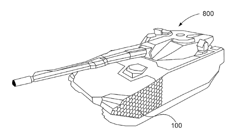
Fig. 3a schematically illustrates a three dimensional view of a number of
surface elements arranged on a platform according to an embodiment of the
present invention.
With reference to fig. 3a it is shown an exploded side view of a platform 800.
The platform is provided with a number of said surface elements, such as
exemplified with reference to fig. 1, externally arranged on a portion of the
platform 800. Said surface element may be arranged in several different
CA 02835160 2013-11-05
WO 2012/169958
PCT/SE2012/050601
17
configurations that differ from the surface elements as exemplified with
reference to fig. 3a. As an example more or fewer surface element may be
part of the configuration and these surface elements may be arranged on
more and/or larger portions of the platform. The exemplified platform 800 is a
military vehicle, such as a motorized combat vehicle. According to this
example the platform is a tank or combat vehicle. According to a preferred
embodiment the vehicle 800 is a military craft. The platform 800 may be a
wheeled vehicle, such as for example a four wheeled, six wheeled or eight
wheeled motor vehicle. The platform 800 may be a tracked vehicle, such as
for example a tank. The platform 800 may be a terrain vehicle of arbitrary
type.
According to an alternative embodiment the platform 800 is a stationary
military unit. Herein the platform 800 is described as a tank or combat
vehicle, it should however be pointed out that is possible to realize and
implement in a naval vessel, such as for example in a surface combat ship.
According to one embodiment the vehicle is a ship such as a combat ship.
According to an alternative embodiment the platform is an airborne vehicle
such as for example an helicopter. According to an alternative embodiment
the platform is a civilian vehicle or other unit according to any of the above
described types.
Fig. 3b schematically illustrates a three dimensional view of functions of a
number of surface elements arranged on a platform according to an
embodiment of the present invention.
With reference to fig. 3b it is shown an exploded side view of a platform 800.
The platform is provided with a number of said surface elements 100, such
as exemplified with reference to fig. la, arranged externally on two portions
of the platform 800 such as a side of a body and a turret of a motorized
combat vehicle 800. Said surface elements may be arranged, in different
configurations differing as compared to the configuration of the exemplified
surface element with reference to fig. 3b. As an example more or fewer
CA 02835160 2013-11-05
WO 2012/169958
PCT/SE2012/050601
18
surface elements may be part of the configuration and these surface
elements may be arranged on more and/or larger portions of the platform.
The vehicle 800 is located in a surrounding that in a perspective of an
observer comprises three background structure BA1-BA3 such as a sky BA1,
a mountain BA2, and a ground-level plan BA3. Said surface elements is
arranged to reproduce said background structures (visually/thermally) BA1-
BA3 by means of utilizing the display surface 50 and/or the temperature
generating element 150 such as described with reference to fig. la.
Fig. 4a schematically illustrates an exploded three dimensional view of a part
II of a part of the device for signature adaptation according to an embodiment
of the present invention.
The device comprises a surface element 300 comprising a control circuit 200,
a housing 510, 520, a first and a second heat conducting layer, an
intermediate heat conducting element 160, a radar suppressing element 190
and a display surface 50 arranged to radiate at least one predetermined
spectrum. The surface element 300 further comprises at least one
temperature generating element 150 arranged to generate at least one
predetermined temperature gradient. The temperature generating element
150, such as formed by a thermoelectric element 150, is arranged to
generate said predetermined temperature gradient to a portion of said first
heat conducting layer 110. The display surface 50 is arranged on said
surface element 300 so that said at least one predetermined spectrum is
radiated in a direction facing an observer.
According to one embodiment the display surface 50 such as for as
described with reference to figure 7a-e is connected to a first housing
element 510 of the surface element 300 using a fastening means such as
glue, screw or other type of suitable fastening means.
The control circuit 200, such as exemplified with reference to fig. 2, is
arranged to be electrically/communicatively connected to at least one of the
CA 02835160 2013-11-05
WO 2012/169958
PCT/SE2012/050601
19
display surface 50 and the temperature generating element 150, wherein the
control circuit 200 is arranged to provide control signal relating to said at
least
one predetermined spectrum and said at least one predetermined
temperature gradient. The surface element 300 according to this embodiment
comprises a housing, wherein said housing comprises a first housing
element 510 and a second housing element 520. The first housing element is
arranged as an upper protective housing. The second housing element 520
is arranged as a base plate and is arranged to be applied using fastening
means to one or more structures and/or elements of a platform or an object
that is desired to be hidden by means of the visual and thermal adaptation
enabled by the system. The first and the second housing elements together
form a substantially impermeable casing of the first heat conducting layer
110, the intermediate insulation layer 130, the control circuit 200 and the
thermoelectric element 150.
The first heat conducting layer 110, which according to a preferred
embodiment is constituted by graphite, is arranged underneath the first
housing element 510. The second heat conducting layer 120 or inner heat
conducting layer 120 is according to a preferred embodiment constituted by
graphite.
The first housing element 510 and the first heat conducting element 110 are
arranged with a frequency selective surface structure, also referred to as a
frequency selective subsurface area 510B, 110B. Said frequency selective
subsurface area 510B, 110B is arranged to surround a subsurface area
510A, 110A of said first housing element 510 and the first heat conducting
element 110. Said subsurface area 510A, 110A is further arranged to be free
of frequency selective surface structure.
According to an embodiment said subsurface area 510A, 110A of said first
housing element 510 and the first heat conducting element 110 is arranged
on a surface opposite to the surface to which said at least one thermoelectric
CA 02835160 2013-11-05
WO 2012/169958
PCT/SE2012/050601
element 150 is arranged. The extension of said subsurface area 510A, 110A
corresponds to the extension of said at least one thermoelectric element 150.
By providing a frequency selective subsurface area transmission of incident
radio waves from radar system is enabled i.e. wherein said radio waves are
5
transmitted/filtered through said first housing element 510 and said first
heat
conducting element 110.
The first heat conducting layer 110 and the second heat conducting layer 120
have anisotropic heat conductibility such that the heat conductibility in the
main direction of propagation, i.e. along the layer 110, 120, is considerably
10 higher than
the heat conductibility crosswise to the layer 110, 120. Hereby
heat or cold may be dispersed quickly on a large surface with relatively few
thermoelectric elements, wherein temperature gradients and hot spots are
reduced. The first heat conducting layer 110 and the second heat conducting
layer 120 are according to an embodiment constituted by graphite.
15 One of the
first heat conducting layer 110 and the second heat conducting
layer 120 is arranged to be a cold layer and another one of the first heat
conducting layer 110 and the second heat conducting layer 120 is arranged
to be a hot layer.
The insulation layer 130 is configured such that heat from the hot heat
20 conducting
layer does not affect the cold heat conducting layer and vice
versa. According to a preferred embodiment the insulation layer 130 a
vacuum based layer. Thereby both radiant heat and convection heat is
reduced.
The thermoelectric element 150 is according to an embodiment arranged in
the insulation layer 130. The thermoelectric element 150 is configured in
such a way that when a voltage is applied, i.e. a current is supplied to the
thermoelectric element 150, heat from one side of the thermoelectric element
150 transcends to the other side of the thermoelectric element 150. The
thermoelectric element 150 is consequently arranged between two heat
CA 02835160 2013-11-05
WO 2012/169958
PCT/SE2012/050601
21
conducting layers 110, 120, e.g. two graphite layers, with asymmetric heat
conductibility in order to efficiently disperse and evenly distribute heat or
cold.
Due to the combination of the two heat conducting layers 110, 120 with
anisotropic heat conductibility and the insulation layer 130 the surface of
the
surface element 100, which according to this embodiment is constituted by
the surface of the first heat conducting layer 110, may by application of
voltage on the thermoelectric element a surface 102 of the surface element
100 be quickly and efficiently adapted. The thermoelectric element 150 is in
thermal contact with the first heat conducting layer 110.
According to an embodiment said intermediate insulation layer 130 is
constituted by a material that enables transmission of incident radio waves
from a radar system.
According to an embodiment the device comprises an intermediate heat
conducting element 160 arranged in the insulation layer 130, the control
circuit 200 and the second housing element 520 inside of the thermoelectric
element 150 for filling the space between the thermoelectric element 150 and
the second heat conducting element 120. This in order to facilitate more
efficient heat conduction between the thermoelectric element 150 and the
second heat conducting element 120. The intermediate heat conducting layer
has anisotropic heat conductibility where the heat conduction is considerably
better crosswise to the element than along the element, i.e. it is conducting
heat considerably better crosswise to the layers of the surface element 100.
This is apparent from fig. 4b. According to an embodiment the intermediate
heat conducting element 160 is constituted by graphite with the
corresponding properties as the first and second heat conducting layer 110,
120 but with anisotropic heat conduction in a direction perpendicular to the
heat conduction of the first and second heat conducting layer 110, 120.
According to one embodiment the intermediate heat conducting element 160
is arranged in an aperture arranged to receive said intermediate heat
conducting element 160. Said aperture is arranged to extend through the
CA 02835160 2013-11-05
WO 2012/169958
PCT/SE2012/050601
22
intermediate insulation layer 130, the control circuit 200 and the second
housing element 520.
Further the insulation layer 130 could be adapted in thickness for the
thermoelectric element 150 such that there is no space between the
thermoelectric element 150 and the second heat conducting element 120.
According to an embodiment the first heat conducting layer 110 has a
thickness in the range of 0.1-2 mm, e.g. 0.4-0.8 mm, the thickness depending
among others depending on application and desired heat conduction and
efficiency. According to an embodiment the second heat conducting layer
120 has a thickness in the range of 0.1-2 mm, e.g. 0.4-0.8 mm, the thickness
depending among others on application and desired heat conduction and
efficiency.
According to an embodiment the insulation layer 130 has a thickness in the
range of 1-30 mm, e.g. 10-20 mm, the thickness depending among others on
application and desired efficiency.
According to an embodiment the thermoelectric element 150 has a thickness
in the range of 1-20 mm, e.g. 2-8 mm, according to a variant about 4 mm, the
thickness depending among others on the application and desired heat
conduction and efficiency. The thermoelectric element has according to an
embodiment a surface in the range of 0.01 mm2- 200 cm2.
The thermoelectric element 150 has according to an embodiment a squared
or other arbitrary geometric shape, such for example hexagonal shape.
The intermediate heat conducting element 160 has a thickness being
adapted such that it fills the space in the space between the thermoelectric
element 150 and the heat conducting layer 120.
The first and second housing element has according to an embodiment a
thickness in the range of 0,2-4 mm, e.g. 0,5-1 mm and depends among
others on the application and efficiency.
CA 02835160 2013-11-05
WO 2012/169958
PCT/SE2012/050601
23
According to an embodiment the surface of the surface element 100 is in the
range of 25-8000 cm2, e.g. 75-1000 cm2. The thickness of the surface
element is according to an embodiment in the range of 5-60 mm, e.g. 10-25
mm, the thickness depending among others on the application and desired
heat conduction and efficiency.
Fig. 4b. schematically illustrate an exploded side view flows of the part III
of a
device for signature adaptation according to an embodiment of the present
invention.
The device comprises a surface element 300 arranged to assume a
determined thermal distribution, wherein said surface element comprises a
housing, wherein said housing comprises a first housing element 510 and a
second housing element 520, a first heat conducting layer 110, a second
heat conducting layer 120, wherein said first and second heat conducting
layers are mutually isolated by means of an intermediate insulation layer 130,
and a thermoelectric element 150 arranged to generate a predetermined
temperature gradient of a portion of said first heat conducting layer 110. The
device further comprises at least one display surface 50 arranged to radiate
at least one predetermined spectrum. The device also comprises an
intermediate heat conducting element 160, such as for example described
with reference to fig. 4a.
The surface element 300 according to certain embodiments, see e.g. fig. 6a,
comprises additional layers for e.g. applying of a surface element 300 to a
vehicle. Here a third layer 310 and a fourth layer 320 are arranged for
further
diversion of heat and/or thermal contact to surface of e.g. vehicles.
As apparent from fig. 4b the heat is transported from one side of the
thermoelectric element 150 and transcends to the other side of the
thermoelectric element and further through the intermediate heat conducting
layer 160, heat transport being illustrated with white arrows A or non-filled
arrows A and transport of cold is illustrated with black arrows B or filled
CA 02835160 2013-11-05
WO 2012/169958
PCT/SE2012/050601
24
arrows B, transport of cold physically implies diversion of heat having the
opposite direction to the direction for transport of cold. Here it is apparent
that
the first and second heat conducting layer 110, 120, which according to an
embodiment are constituted by graphite, have anisotropic heat conductibility
such that the heat conductibility in the main direction of propagation, i.e.
along the layer 110, 120, is considerably higher than the heat conductibility
crosswise to the layer. Hereby heat or cold may be dispersed quickly on a
large surface with relatively few thermoelectric elements and relatively low
supplied power, whereby temperature gradients and hot spots are reduced.
Further an even and constant desired temperature may be kept during a
longer time.
Heat is transported further through the third layer 310 and the fourth layer
320 for diversion of heat.
As further apparent from fig. 4b at least one spectrum comprising light of one
or more wavelengths/frequencies is radiated from said at least one display
surface 50, wherein said radiated light is illustrated with dashed arrows D.
Heat is transported from the first heat conducting layer 110 up into the first
housing element and through said at least one display surface 50, which is
arranged to have a thermal permeability. Hereby is facilitated a decoupling
between the thermal and visual signature that is generated i.e. the thermal
signature do not substantially affect the visual signature and vice versa.
With further reference to fig. 4b incident radio within a predetermined
frequency range are transmitted through the frequency selective surface that
is formed in the first housing element 510 and in the first heat conducting
layer 110 and through the intermediate insulation layer 130 in order to
subsequently substantially be absorbed by the radar suppressing element
190.
CA 02835160 2013-11-05
WO 2012/169958
PCT/SE2012/050601
Fig. 5 schematically illustrates an exploded side view of a part IV of a
device
for signature adaptation according to an embodiment of the present
invention.
The device according to this embodiment differs from the embodiment
5 according to fig. 4a only in that it comprises a housing, a first heat
conducting
layer, a second heat conducting layer, an intermediate insulation layer, a
radar suppressing element, a display surface and three thermoelectric
elements arranged on top of each other instead of that it comprises a
housing, a first heat conducting layer, a second heat conducting layer, an
10 intermediate insulation layer, a radar suppressing element a temperature
generating element and a display surface.
The device comprises a surface element 400 arranged to assume a
determined thermal distribution and to radiate at least one predetermined
spectrum, wherein said surface element 400 comprises a first housing
15 element 510 and a second housing element 520, a display surface 50, a
first
heat conducting layer 110, a second heat conducting layer 120, wherein said
first and second heat conducting layers 110, 120 are mutually isolated by
means of an intermediate insulation layer 130, and a thermoelectric element
configuration 450 arranged to generate a predetermined temperature
20 gradient to a portion of said first heat conducting layer 110.
According to an embodiment the device comprises an intermediate heat
conducting layer 160 arranged in the insulation layer 130 inside of the
thermoelectric element 150 to fill possible space between the thermoelectric
element configuration 450 and the second heat conducting element 120. This
25 in order for that heat conduction may occur more efficiently between the
thermoelectric element configuration 450 and the second heat conducting
element 120. The intermediate heat conducting element 160 has anisotropic
heat conductibility, the heat conduction being considerably better crosswise
to than along the element, i.e. conducts heat considerably better crosswise to
CA 02835160 2013-11-05
WO 2012/169958
PCT/SE2012/050601
26
the layers of the surface element 100, in accordance with what is illustrated
in fig. 4a.
The thermoelectric element configuration 450 comprises three thermoelectric
elements 450a, 450b, 450c arranged on top of each other. A first
thermoelectric element 450a being arranged outermost in the insulation layer
of the surface element 400, a second thermoelectric element 450b, and a
third thermoelectric element 450c being arranged innermost, wherein the
second thermoelectric element 450b is arranged between the first and the
third thermoelectric element.
When voltage is applied as the outer surface 402 of the surface element 400
is intended to be cooled such that heat is transported by means of the first
thermoelectric element 450a from the surface and toward the second
thermoelectric element 450b. The second thermoelectric element 450b is
arranged to transport heat from its outer surface towards the third
thermoelectric element 450c such that the second thermoelectric element
450b contributes to transporting excessive heat away from the first
thermoelectric element 450a. The third thermoelectric element 450c is
arranged to transport heat from its outer surface towards the second heat
conducting layer 120, via the intermediate heat conducting element 160,
such that the third thermoelectric element 450c contributes in transporting
excessive heat away from the first and second thermoelectric elements.
Hereby a voltage is applied over the respective thermoelectric element 450a,
450b, 450c.
Here an intermediate heat conducting element is arranged between the
thermoelectric element configuration 450 and the second heat conducting
element 120. Alternatively the thermoelectric element configuration 450 is
arranged to fill the entire insulation layer such that no intermediate heat
conducting element is required.
CA 02835160 2013-11-05
WO 2012/169958
PCT/SE2012/050601
27
The respective thermoelectric element 450a, 450b, 450c has according to an
embodiment a thickness in the range of 1-20 mm, e.g. 2-8 mm, according to
a variant about 4 mm, the thickness depending among others on application
and desired heat conduction and efficiency.
The insulation layer 130 according to an embodiment has a thickness in the
range of 4-30 mm, e.g. 10-20 mm, the thickness depending among other on
application and desired efficiency.
By using three thermoelectric elements arranged on top of each other as in
this example, the net efficiency of heat transported away becomes higher
than by using only on thermoelectric element. Hereby diversion of heat is
rendered more efficient. This may e.g. be required during intense heat from
the sun in order to efficiently divert heat.
Alternatively two thermoelectric elements arranged on top of each other may
be used, or more than three thermoelectric elements arranged on top of each
other.
Fig. 6a schematically illustrated in an exploded three dimensional view a part
V of a device for signature adaptation according to an embodiment of the
present invention.
Fig. 6b schematically illustrated in an exploded side view a part V of a
device
for signature adaptation according to an embodiment of the present invention
suitable for use on for example a military vehicle for signature adaptation
The device comprises a surface element 500 arranged to assume a
determined thermal distribution, wherein said surface element 500 comprises
a housing, wherein said housing comprises a first housing element 510 and a
second housing element 520, a first and second heat conducting layer 110,
120 wherein said first and second heat conducting layers 110, 120 are
mutually heat insulated by means of a first intermediate insulation layer 131
and a second intermediate insulation layer 132, a control circuit 200, an
CA 02835160 2013-11-05
WO 2012/169958
PCT/SE2012/050601
28
interface material 195, an armouring element 180, a radar suppressing
element 190, a thermoelectric element 150 arranged to generate a
predetermined temperature gradient to a portion of said first heat conducting
layer 110 and a display surface 50 arranged to radiate at least one
predetermined spectrum.
The module element 500 constitutes according to a variant a part of the
device which is interconnected by module elements, the module elements
according to an embodiment being constituted by module elements
according to fig. 6a-b, wherein the module element forms a module system
as shown in fig. 12a-c for application on e.g. a vehicle.
The module element 500 according to this embodiment comprises a housing,
wherein said housing comprises a first housing element 510 and a second
housing element 520. The first housing element 510 is arranged as an upper
protective casing. The second housing element is arranged as a base plate
and is arranged to be applied, such as for example as described with
reference to fig. 12a-g, by means of fastening means to one or more
structures and/or elements of a platform such as an object desired to be
hidden by means of the visual and thermal adaptation enabled by the
system. The first and second housing element together for a substantially
impermeable casing of the first heat conducting layer 110, the first
intermediate insulation layer 131 and the second intermediate insulation layer
132, the control circuit 200, the interface material 195, the armouring
element
180, the radar suppressing element 190 and the thermoelectric element 150.
The housing is composed of a material with efficient heat conductibility for
conducting heat or cold from an underlying layer in order to facilitate
representing the thermal structure, which according to an embodiment is a
copy of the thermal background temperature. According to an embodiment
the first housing element 510 and the second housing element 520 is made
of aluminium, which has an efficient thermal conductibility and is robust and
CA 02835160 2013-11-05
WO 2012/169958
PCT/SE2012/050601
29
durable which results in a good outer protection and consequently renders
suitable for cross country vehicles.
The module element 500 according to this embodiment comprises at least
one display surface 50, such as exemplified with reference to fig. 7a-e. Said
at least one display surface is arranged on the upper side of the first
housing
element 510 such as for example arranged on the upper side of the first
housing element by means of fastening means such as fastened by glue or
screws.
The first heat conducting layer 110, which according to a preferred
embodiment is constituted by graphite, is arranged under the outer layer 510.
The second heat conducting layer 120 or inner heat conducting layer 120 is
according to a preferred embodiment constituted by graphite.
The first heat conducting layer 110 and the second heat conducting layer 120
have anisotropic heat conductibility. Thus, the first and the second heat
conducting layers respectively has such a composition and such properties
that the longitudinal heat conductibility, i.e. heat conductibility in the
main
direction of propagation along the layer is considerably higher than the
transversal heat conductibility, i.e. the heat conductibility crosswise to the
layer, the heat conductibility along the layer being good. These properties
are
facilitated by means of graphite layers with layers of pure carbon, which is
achieved by refinement such that higher anisotropy of the graphite layers is
achieved. Hereby heat may be dispersed quickly on a large surface with
relatively few thermoelectric elements, whereby temperature gradients and
hot spots are reduced.
According to a preferred embodiment the ratio between longitudinal heat
conductibility and transversal heat conductibility of the layer 110, 120 is
greater than hundred. With increasing ratio it is facilitated to having the
thermoelectric elements arranged on a larger distance from each other,
which results in a cost efficient composition of module elements. By
CA 02835160 2013-11-05
WO 2012/169958
PCT/SE2012/050601
increasing the ratio between the heat conductibility along the layer 110, 120
and heat conductibility crosswise to the layers 110, 120 the layers may be
made thinner and still obtain the same efficiency, alternatively make the
layer
and thus the module element 500 quicker.
5 One of the
first and second heat conducting layers 110, 120 is arranged to be
a cold layer and another of the first and second heat conducting layers 110,
120 is arranged to be a hot layer. According to an application e.g. for
camouflaging of vehicles, the first heat conducting layer 110, i.e. the outer
of
the heat conducting layers, is the cold layer.
10 The graphite
layers 110, 120 has according to a variant a composition such
that the heat conductibility along the graphite layer is in the range of 300-
1500 W/mK and the heat conductibility crosswise to the graphite layer is in
the range of 1-10 W/mK.
According to an embodiment the module element 500 comprises an
15 intermediate
heat conducting element 160 arranged inside the housing.
Where said intermediate heat conducting element 160 further is arranged to
extend through an aperture centrally positioned in underlying
layers/elements, said aperture arranged to receive the intermediate heat
conducting element 160. Said aperture is arranged to partially or fully extend
20 through the
first insulation layer 131, the second insulation layer 132, the
radar suppressing layer 190, the armouring element 180, the control circuit
200, the interface material 195 and the second housing element 520 to fill
possible space between the thermoelectric element 150 and the second heat
conducting element 120. This so that heat conducting may occur more
25 efficiently
between the thermoelectric element 150 and the second heat
conducting element 120. The intermediate heat conducting element has
anisotropic heat conductibility wherein the heat conduction is considerably
better along the layers than crosswise to the layers of the surface element
300. This is apparent from fig. 4b. According to an embodiment the
30 intermediate
heat conducting element 160 is constituted by graphite with
CA 02835160 2013-11-05
WO 2012/169958
PCT/SE2012/050601
31
corresponding properties as of the first and second heat conducting layer
110, 120 but with anisotropic heat conduction in a direction perpendicular to
the heat conduction of the first and second heat conducting layers 110, 120.
The first and second insulation layers for thermal isolation is arranged
.. between the first heat conducting layer 110 and the second heat conducting
layer 120. The insulation layers are configured such that heat from the hot
heat conducting layer 110, 120 minimally affects the cold heat conducting
layer 120, 110 and vice versa. The insulation layers 131, 132 considerably
improves performance of the module element 500/device. The first heat
conducting layer 110 and the second heat conducting layer 120 are mutually
thermally isolated by means of the intermediate insulation layers 131, 132.
The thermoelectric element 150 is in thermal contact with the first heat
conducting layer 110.
The first housing element 510 and the first heat conducting element 110 are
arranged with a frequency selective surface structure, also referred to as a
frequency selective subsurface area 510B, 110B. Said frequency selective
subsurface area 510B, 110B is arranged to surround a subsurface area
510A, 110A of said first housing element 510 and the first heat conducting
element 110. Said subsurface area 510A, 110A is further arranged to be free
of frequency selective surface structure.
According to an embodiment said subsurface area 510A, 110A of said first
housing element 510 and the first heat conducting element 110 is arranged
on a surface opposite to the surface to which said at least one thermoelectric
element 150 is arranged. The extension of said subsurface area 510A, 110A
corresponds to the extension of said at least one thermoelectric element 150.
According to an embodiment said subsurface area 510A, 110A of said first
housing element 510 and the first heat conducting element 110 is arranged
on a surface opposite to the surface to which said at least one thermoelectric
CA 02835160 2013-11-05
WO 2012/169958
PCT/SE2012/050601
32
element 150 is arranged. The extension of said subsurface area 510A, 110A
corresponds to the extension of said at least one thermoelectric element 150.
According to an embodiment said radar suppressing element 190 is
integrated in said first heat conducting layer 110. According to this
embodiment the surface element 500 does not comprise any separate radar
suppressing element 190. According to this embodiment said first heat
conducting layer 110 further does not comprise any frequency selective
surface structure. According to this embodiment said first heat conducting
layer 110 is formed of a material that enables both good heat transmission
properties and radar absorbing properties such as for example graphite.
According to this embodiment the entire surface of said first housing element
510 is provided with frequency selective surface structure so that incident
radio waves are filtered and where the filtered radio waves that are
transmitted through the first housing element are suppressed by the
underlying heat conducting layer 110. According to this embodiment said
control circuit may further be arranged to provide control signals to said at
least one thermoelectric element 150 to compensate for possible heating that
may occur in said first heat conducting layer 110 due to absorption of
incident
filtered radio waves. This may for example be achieved by utilizing
information from the temperature sensing means 210. By providing radar
suppressive functionality in said first heat conducting layer 110 it is
achieved
that the surface element 500 efficiently may absorb incident radio waves over
its entire surface and not only the surface surrounding said at least one
thermoelectric element. Furthermore it is facilitated to construct the surface
element so it becomes thinner and lighter since need for a separate radar
suppressing element is rendered un-necessary.
According to an embodiment the first insulation layer 131 is arranged
between the first heat conducting element 110 and the radar suppressing
element 190.
CA 02835160 2013-11-05
WO 2012/169958
PCT/SE2012/050601
33
According to an embodiment said first intermediate insulation layer 131 is
constituted by a material that enables transmission of incident radio waves
from a radar system.
According to an embodiment the second insulation layer 132 is arranged
between the armouring element 180 and the control circuit 200.
According to an embodiment at least one of the first and second insulation
layers 131, 131, such as for example the first insulation layer 131, is a
vacuum based element 530 or a vacuum based layer 530. Hereby both
radiant heat and convection heat are reduced due to interaction between
material, which is relatively high in conventional insulation materials having
a
high degree of confined air, i.e. porous materials such as foam, glass fibre
fabric, or the like, occurs to a very low degree, the air pressure being in
the
range of hundred thousand times lower than conventional insulation
materials.
According to an embodiment the vacuum based element 530 is covered with
high reflection membranes 532. Thereby transport of heat in the form of
electromagnetic radiation, which does not need to interact with material for
heat transportation, is counteracted.
The vacuum based element 530 consequently results in very good isolation,
and further has a flexible configuration for different applications, and
thereby
fulfils many valuable aspects where volume and weight are important.
According to an embodiment the pressure in the vacuum based element lies
in the range of 0.005 and 0.01 torr.
According to an embodiment at least one of the first and second insulation
layers 131, 132, such as for example the first insulation layer 131, comprises
screens 534 or layers 534 with low emission arranged to considerably reduce
the part of the heat transport occurring through radiation. According to an
embodiment at least one of the first and second insulation layers 131, 132,
such as for example the first insulation layer 131, comprises a combination of
CA 02835160 2013-11-05
WO 2012/169958
PCT/SE2012/050601
34
vacuum based element 530 and low emissive layers 534 in a sandwich
construction. This gives a very efficient heat isolator and may give k-values
as good as 0.004 W/mK.
According to an embodiment at least one of the first and second insulation
layers 131, 132 is formed of a thermally isolating foam material or other
suitable thermally insulating material.
According to an embodiment the first housing element 510 and the first heat
conducting layer 110 are each arranged to provide a frequency selective
surface 535, 536 such as exemplified with reference to fig. 8.
The radar suppressing element 190 is according to an embodiment arranged
between the first insulation layer 131 and the armouring element 180.
The armouring element 180 such as exemplified with reference to fig. 9 is
according to an embodiment arranged between the radar suppressing
element and the second insulation layer 132.
The control circuit 200 is according to an embodiment arranged between the
second insulation layer 132 and the interface material 195. Where the control
circuit is arranged to provide control signals/voltage/current to said at
least
one display surface and said thermoelectric element 150.
The interface material 195 is according to an embodiment arranged between
the control circuit 200 and the second housing element 520. The interface
material 195 is arranged to provide means for fastening the control circuit
200 to the second housing element 520 and to conduct heat from the control
circuit 200 to the second housing element 520. By providing an interface
material 195 as described above it is facilitated to efficiently conduct heat
away from the control circuit so that the control circuit is prevented from
overheating and so that it do not affect the upper layers when these are
intended to be cooled.
CA 02835160 2013-11-05
WO 2012/169958
PCT/SE2012/050601
The module element 500 further comprises a temperature sensing means
210, which according to an embodiment is constituted by a thermal sensor.
The temperature sensing means 210 is arranged to sense the present
temperature. According to a variant the temperature sensing means 210 is
5 arranged to measure a voltage drop through a material being arranged
outermost on the sensor, said material having such properties that it changes
resistance depending on temperature. According to an embodiment the
thermal sensor comprises two types of metals which in their boundary layers
generate a weak voltage depending on temperature. This voltage arises from
10 the Seebeck-effect. The magnitude of the voltage is directly
proportional to
the magnitude of this temperature gradient. Depending on which temperature
range measurements are to be performed different types of sensors are more
suitable than others, where different types of metals generating different
voltages may be used. The temperature is then arranged to be compared to
15 continuous information from a thermal sensing means arranged to
sense/copy the thermal background, i.e. the temperature of the background.
The temperature sensing means 210, e.g. a thermal sensor, is fixed on the
upper side of the first heat conducting layer 110 and the temperature sensing
means in the form of e.g. a thermal sensor may be made very thin and may
20 according to an embodiment be arranged in the first heat conducting
layer,
e.g. the graphite layer, in which a recess for countersinking of the sensor
according to an embodiment is arranged.
The module element 500 further comprises the thermoelectric element 150.
The thermoelectric element 150 is according to an embodiment arranged in
25 the first insulation layer 131. The temperature sensing means 210 is
according to an embodiment arranged in layer 110 and in close connection to
the outer surface of the thermoelectric element 150. A voltage is applied to
the thermoelectric element 150 wherein the thermoelectric element 150 is
configured in such a way that when a voltage is applied, heat from one side
30 of the thermoelectric element 150 transcends into the other side of
the
thermoelectric element 150. When the by means of the sensing means 210
CA 02835160 2013-11-05
WO 2012/169958
PCT/SE2012/050601
36
sensed temperature when compared to the temperature information from the
thermal sensing means differs from the temperature information, the voltage
to the thermoelectric element 150 is arranged to be regulated such that
actual values correspond to reference values, wherein the temperature of the
module element 500 is adapted accordingly by means of the thermoelectric
element 150.
The thermoelectric element is according to an embodiment a semiconductor
functioning according to the Peltier effect. The Peltier effect is a
thermoelectric phenomena arising when a dead current is allowed to float
over different metals or semiconductors. In this way a heat pump cooling one
side of the element and heating the other side may be created. The
thermoelectric element comprises two ceramic plates with high thermal
conductivity. The thermoelectric element according to this variant further
comprises semiconductor rods which are positively doped in one end and
negatively doped in the other end such that when a current is flowing though
the semiconductor, electrons are forced to stream such that one side
becomes hotter and the other side colder (deficiency of electrons). During
change of direction of current, i.e. by changed polarity of the applied
voltage,
the effect is the opposite, i.e. the other side becomes hot and the first
cold.
This is the so called Peltier effect, which consequently is being utilized in
the
present invention.
According to an embodiment the module element 500 further comprises a
third heat conducting layer (not shown) in the form of a heat pipe layer or
heat plate layer arranged beneath the second heat conducting layer 120 for
dispersing heat for efficiently divert excessive heat. The third heat
conducting
layer, i.e. the heat pipe layer/heat plate layer comprises according to a
variant sealed aluminium or copper with internal capillary surfaces in the
shape of wicks, the wicks according to a variant being constituted by sintered
copper powder. The wick is according to a variant saturated with liquid which
under different processes either is vaporized or condensed. Type of liquid
CA 02835160 2013-11-05
WO 2012/169958
PCT/SE2012/050601
37
and wick is determined by the intended temperature range and determines
the heat conductibility.
The pressure in the third heat conducting layer, i.e. the heat pipe layer/
heat
plate layer is relatively low, wherefore the specific steam pressure makes the
liquid in the wick vaporizing in the point in which heat is applied. The steam
in
this position has a considerably higher pressure than its surrounding which
results in it dispersing quickly to all areas with lower pressure, in which
areas
it condenses into the wick and emits its energy in the form of heat. This
process is continuous until an equilibrium pressure has arisen. This process
is at the same time reversible such that even cold, i.e. lack of heat can be
transported with the same principle.
The advantage of using layers of heat pipes/ heat plate is that they have very
efficient heat conductibility, substantially higher than e.g. conventional
copper. The ability to transport heat, so called Axial Power Rating (APC), is
impaired with the length of the pipe and increases with its diameter. The heat
pipe/ heat plate together with the heat conducting layers facilitate quick
dispersal of excessive heat from the underside of the module elements 500
to underlying material due to their good ability to distribute heat on large
surfaces. By means of heat pipe/heat plate quick diversion of excessive heat
which e.g. is required during certain sunny situations is facilitated. Due to
the
quick diversion of excessive heat efficient work of the thermoelectric element
150 is facilitated, which facilitates efficient thermal adaptation of the
surrounding continuously.
According to this embodiment the first heat conducting layer and the second
heat conducting layer are constituted by graphite layers such as described
above and the third heat conducting layer is constituted by heat pipe
layers/heat plate layers. According to a variant of the invention the third
heat
conducting layer may be omitted, which results in a slightly reduced
efficiency but at the same time reduces costs. According to an additional
variant the first and/or the second heat conducting layer may be constituted
CA 02835160 2013-11-05
WO 2012/169958
PCT/SE2012/050601
38
by heat pipe layer/ heat plate layer, which increase the efficiency but at the
same time increases the costs. In case the second heat conducting layer is
constituted by heat pipe layer / heat plate layer the third heat conducting
layer may be omitted.
According to an embodiment the module element 500 further comprises a
thermal membrane (not shown). According to this embodiment the thermal
membrane is arranged underneath the third heat conducting layer. The
thermal membrane facilitates good thermal contact on surfaces with small
irregularities such as body of motor vehicles which irregularities otherwise
may result in impaired thermal contact. Hereby the possibility to divert
excessive heat and thus efficient work of the thermoelectric element 150 is
improved. According to an embodiment the thermal membrane is constituted
by a soft layer with high thermal conductivity which results in the module
element 500 obtaining good thermal contact against e.g. the body of the
vehicle, which facilitates good diversion of excessive heat.
Above, the module element 500 and its layers have been described as flat.
Other alternative shapes/configurations are also conceivable. Further other
configurations than those that have been described relating to relative
placement of the elements/layers of the module element are conceivable.
Further other configurations than those that have been described relating to
number of element/layers and their respective function are conceivable.
The first heat conducting layer 110 has according to an embodiment a
thickness in the range of 0.1-2 mm, e.g. 0.4-0.8 mm, the thickness among
others depending on application and desired heat conduction and efficiency.
The second heat conducting layer 120 has according to an embodiment a
thickness in the range of 0.1-2 mm, e.g. 0.4-0.8 mm, the thickness among
others depending on application and desired heat conduction and efficiency.
CA 02835160 2013-11-05
WO 2012/169958
PCT/SE2012/050601
39
The first and second insulation layers 131, 132 have according to an
embodiment a thickness in the range of 1-30 mm, e.g. 2-6 mm, the thickness
among others depending on application and desired efficiency.
The thermoelectric element 150 has according to an embodiment a thickness
in the range of 1-20 mm, e.g. 2-8 mm, according to a variant about 4 mm, the
thickness among other depending on application and desired heat
conduction and efficiency. The thermoelectric element according to an
embodiment has a surface in the range of 0.01 mm2-200 cm2.
The intermediate heat conducting element 160 has a thickness being
adapted such that it fills the space between the thermoelectric element 150
and the second heat conducting layer 120. According to an embodiment the
intermediate heat conducting element has a thickness in the range of 5-30
mm, e.g. 10-20 mm, according to a variant 15 mm, the thickness among
others depending on application and desired heat conduction and efficiency.
The first and second housing element according to an embodiment have a
thickness in the range of 0.2-4 mm, e.g. 0,5-1 mm and depends among
others on application and efficiency.
The thermal membrane according to an embodiment has a thickness in the
range of 0.05-1 mm, e.g. about 0.4 mm and depends among others on
application.
The third heat conducting layer in the shape of a heat pipe/ heat plate
according to above has according to an embodiment a thickness in the range
of 2-8 mm, e.g. about 4 mm, the thickness among others depending on
application, desired efficiency and heat conduction.
The surface of the module element/ surface element 500 is according to an
embodiment in the range of 25-2000 cm2, e.g. 75-1000 cm2. The thickness of
the surface element is according to an embodiment in the range of 5-60 mm,
CA 02835160 2013-11-05
WO 2012/169958
PCT/SE2012/050601
e.g. 10-25 mm, the thickness among others depending on desired heat
conduction and efficiency, and materials of the different layers.
Fig. 7a schematically illustrates a side view of the display surface according
to an embodiment of the present invention.
5 According to an embodiment the display surface 50 is of emitting type. By
display surface of emitting type is intended a display surface that actively
generates and radiates light LE. Examples of display elements of emitting
type is for example a display surface that uses any of the following
techniques: LCD ("Liquid Crystal Display"), LED ("Light Emitting Diode"),
10 OLED ("Organic Light emitting Diode") or other suitable emitting
technology
that is based on both organic or non-organic electro-chrome technology or
technology similar thereto.
Fig. 7b schematically illustrates a side view of the display surface according
to an embodiment of the present invention.
15 According to a preferred embodiment the display surface 50 is of reflecting
type. By display surface of reflecting type is intended a display surface
arranged to receive incident light LI and radiate reflected light LR by means
of using said incident light LI. Examples of display elements of emitting type
is for example a display surface that uses any of the following techniques:
20 ECI ("Electrically Controllable Organic Electro chromes"), ECO
("Electrically
Controllable Inorganic Electro chromes"), or other suitable reflecting
technology such as "E-ink", electrophoretic, cholesteric, MEMS (Micro
Electro-Mechanical System) coupled to one or more optical films, or electro
fluidic. By utilizing a display surface 50 of reflecting type it is enabled to
25 produce at least one spectrum that realistically reflects
structures/colours
since this type uses naturally incident light instead of self producing light
such
as for example display surfaces of emitting type such an LCD do. Common
for a display surface of a reflecting type is that an applied voltage enables
modification of reflection properties for each individual picture element Pl-
CA 02835160 2013-11-05
WO 2012/169958
PCT/SE2012/050601
41
P4. By controlling the applied voltage for each picture element each picture
element is thereby enabled to reproduce a certain colour upon reflection of
incident light that is dependent on the applied voltage.
According to an alternative embodiment the display surface 50 is of reflecting
and emitting type such as multi-modal liquid crystal (Multimode LCD). Where
said display surface 50 according to this embodiment is arranged to both
emit at least one spectrum and reflect at least one spectrum.
Fig. 7c schematically illustrates a top view of the display surface according
to
an embodiment of the present invention.
The display surface 50 comprises a plurality of picture elements ("pixels") P1-
P4, wherein said picture elements P1-P4 each comprises a plurality of sub
elements ("sub-pixels") S1-S4. Said picture elements P1-P4 have an
extension in height H and an extension in width W.
According to an embodiment the picture elements each have an extension in
height H in the range of 0.01-100 mm, e.g. 5-30 mm.
According to an embodiment the picture elements each have an extension in
width W in the range of 0.01-100 mm, e.g. 5-30 mm.
According to an embodiment each picture element P1-P4 comprises at least
three sub elements S1-54. Where each of said at least three sub elements is
arranged to radiate one of the primary colours red, green or blue (RGB) or
the secondary colours cyan, magenta, yellow or black (CMYK). By controlling
the light intensity that is radiated from the respective sub element using
control signals each picture element may radiate any colour/spectrum such
as for example black or white.
According to an embodiment each picture element P1-P4 comprises at least
four sub elements S1-S4. Where each of said four sub elements is arranged
to radiate one of the primary colours red, green or blue (RGB) or the
secondary colours cyan, magenta, yellow or black (CMYK) and wherein one
CA 02835160 2013-11-05
WO 2012/169958
PCT/SE2012/050601
42
of said four sub elements is arranged to radiate one or more spectrums that
comprises components falling outside of the visual wave lengths such as for
example arranged to radiate one or more spectrums that comprises
components within the infrared wave lengths. By radiating one or more
spectrum comprising components falling within the infrared area and one or
more components falling within the visual area it is enabled to apart from
controlling the visual signature to also control the thermal signature using
the
components falling within the infrared area. This facilitates shortening the
response time associated to adapting the thermal signature using said
thermoelectric element 150.
Said display surface may be arranged according to several different
configurations differing as compared to the exemplified display surface with
reference to fig. 7c. As an example more or fewer picture elements may be
part of the configurations and these picture elements may comprise more or
fewer sub elements.
The display surface is according to one embodiment constituted by thin film,
such as for example thin film substantially constituted by polymer material.
Said thin film may comprise one or more active and/or passive layers/thin
layers and one or more components such as electrically responsive
components/layers or passive/active filters.
The display surface 50 is according to one embodiment constituted by
flexible thin film.
The display surface 50 according to an embodiment has a thickness in the
range of 0.01-5 mm, e.g. 0.1-0.5 mm and depends among others on
application and desired efficiency.
According to an embodiment the picture elements P1-P4 of the display
surface 50 has a width in the range of 1-5 mm, e.g. 0.5-1.5 mm and a height
in the range of 1-5 mm, e.g. 0.5-1.5 mm, wherein the dimensioning among
others depending on application and desired efficiency.
CA 02835160 2013-11-05
WO 2012/169958
PCT/SE2012/050601
43
According to an embodiment the display surface 50 has a thickness in the
range of 0.05-15 mm, e.g. 0.1-0.5 mm, according to a variant about 0.3 mm,
wherein the thickness among others depending on application and thermal
permeability, colour reproduction and efficiency.
According to an embodiment the display surface 50 is configured to have an
operating temperature range that comprises the temperature range in which
thermal adaptation is desired to be performed, such as for example within -
20-150 C. This facilitates that reproduction of at least one predetermined
spectrum for desired visual adaptation is substantially un-affected by desired
temperature for thermal adaptation from underlying layers.
According to an embodiment the display surface 50 is of emitting type and
arranged to provide directionally dependent reflection. As an example each
picture element of the display surface 50 may be arranged to alternately
provide at least two different spectrums. This may be accomplished by
providing at least two of each other independent control signals such that
each picture element reproduces at least two different spectrums at least two
different points in time, defined by one or more update frequencies.
Fig. 7d schematically illustrates a side view of a display surface according
to
an embodiment of the present invention.
According to an embodiment the display surface 50 is of reflecting type and
arranged to provide directionally dependent reflection. According to this
embodiment the display surface comprises at least one first underlying
display layer 51 and a second upper display layer 52. Said first display layer
51 is arranged as a reflective layer comprising at least one curved reflective
surface 53. According to this embodiment the profile of said at least one
curved reflective surface is formed as a number of trapezoids. Said second
display layer 52 is arranged as an obstructing layer comprising at least one
optical filter structure, 55, 56, wherein said at least one filter structure
is
arranged to obstruct incident light of selected angles of incidence and
CA 02835160 2013-11-05
WO 2012/169958
PCT/SE2012/050601
44
thereby obstruct reflection from the first display layer 51. Said curved
reflective surface 53 comprises a plurality of sub surfaces 51A-F, each
arranged to reflect incident light within a predetermined angular range or in
a
predetermined angle. According to this embodiment the curved reflective
surface 53 comprises a first sub surface 51B and a second sub surface 51E
arranged substantially parallel to the plane constituted by the display
surface.
Said first and second subsurface are arranged to reflect light, substantially
incident orthogonally to the display surface 50. The curved reflective surface
53 further comprises a third sub surface 51A, a fourth sub surface 510, a
fifth
sub surface 51D and a sixth sub surface 51F. Said fourth and sixth sub
surfaces 51C, 51F are arranged to reflect light, incident within a
predetermined angular range, that is displaced in a first predetermined angle
01, relative the orthogonal axis. Said third and fifth sub surfaces 51A, 51D
are arranged to reflect light, incident within a predetermined angular range,
that is displaced in a second predetermined angle 02, relative the orthogonal
axis, wherein said first predetermined angle falls on an opposite side of the
orthogonal axis relative said second predetermined angle.
According to an embodiment the obstructing layer comprises at least one first
filter structure 55. Where said at least one first filter structure 55 is
arranged
as a triangle having an extension along a vertical direction of the display
surface i.e. shaped as a triangular prism.
According to an embodiment the obstructing layer comprises at least one
second filter structure 56, wherein said at least one second filter structure
56
is arranged as a plurality of taps/rods having an extension along an
orthogonal direction of the display surface, wherein the length of said at
least
one second filter structure 56 is configured so as to avoid obstructing light,
incident within said predetermined angular range, that is displaced in a first
predetermined angle relative the orthogonal axis and light, incident within
said predetermined angular range, that is displaced in a second
predetermined angle relative the orthogonal axis. This facilitates limiting
the
CA 02835160 2013-11-05
WO 2012/169958
PCT/SE2012/050601
angular range within which reflection of light, incident substantially
orthogonal
towards the display surface takes place.
Fig. 7e schematically illustrates a plan view of parts of the display surface
according to an embodiment of the present invention.
5 According to
an embodiment said curved reflective surface 53 is arranged to
form a three dimensional pattern, wherein said three dimension pattern
comprises a number of columns and a number of rows of truncated
pyramids, i.e. a matrix of pyramids where an upper structure of the pyramids
have been cut in a plane, parallel to the bottom surface of the pyramid.
10 According to
this embodiment said at least one first filter structure 55 of the
obstructing layer 52 is formed as a central pyramid surrounded by truncated
pyramids, whose tapered direction of extensions are opposite to the
truncated pyramids of the reflecting layer. A centre point of the obstructing
layer that is defined by the position of the top of the centrally positioned
15 pyramid with
associated truncated pyramids arranged along the sides of the
centrally positioned is arranged to be centered above the intersection point
that is formed between the rows and the columns of truncated pyramids of
the reflection layer 53, such as illustrated by the dashed arrow in figure 7e.
By means of arranging the curved reflecting surface 53 and the filter
20 structures 55 as described above, slits orthogonal to the respective
subsurface of said reflecting surface are formed that are free of obstruction,
whereby directionally dependent reflection is enabled, where reflection of the
incident light that falls within said slits is enabled. According to this
embodiment each subsurface 51G-51K formed by the front surfaces of the
25 truncated
pyramids of the curved reflecting layer is arranged to provide at
least one picture element each. This facilitates individually adapted
reflection
of incident light, falling within five different angles of incidence or five
different
ranges of angles of incidence.
By providing a directionally dependent display surface 50 according to figure
30 7d-e is facilitated to reproduce at least one spectrum such as one or more
CA 02835160 2013-11-05
WO 2012/169958
PCT/SE2012/050601
46
patterns and colours in different viewing angles relative an orthogonal axis
of
the display surface. Hereby is also facilitated to radiate different patterns
and
colours in different viewing angles.
The configuration of the display surface 50 may differ from the configuration
described with reference to fig. 7d-e. Placement and configuration of filter
structures of said obstructing layer may as an example be configured
differently. Also the number of filter structures may differ. Said first
display
layer 51 may be arranged as an emitting layer. The display surface 50 may
comprise more or fewer layers. Further interference phenomena's together
with one of more reflection layers, optical retardation layers and one or more
circular polarized or one or more linearly polarized layers in combination
with
one or more quarter wave retardation layers may be utilized to provide
directionally dependent reflection.
According to an embodiment the display surface 50 comprise at least one
barrier layer, wherein said at least one barrier layer is arranged to have
thermal and visual permeability and to be substantially impermeable to
moisture and liquid. By applying the at least one barrier layer to the display
surface robustness and endurance are improved in terms of external
environmental influence.
Fig. 8a schematically illustrates a plan view of a structure of the device for
signature adaptation according to an embodiment of the present invention.
With reference to fig. 8a it is shown a frequency selective display surface
FSS arranged in at least one element/layer of the device.
According to this embodiment the frequency selective surface FSS such
exemplified in figure 6b is integrated in the first housing element 510 and
the
first heat conducting layer 110.
The frequency selective surface FSS may for example be provided by
formation of a plurality of resonant slit elements such as "patches" arranged
CA 02835160 2013-11-05
WO 2012/169958
PCT/SE2012/050601
47
in the first housing element 510 and the first heat conducting element 110 or
arranged as trough structures STR extending through the first housing
element and the first heat conducting layer 110, wherein each of the through
structures SIR for example is formed as crossed dipoles. Said resonant slit
elements are formed in a suitable geometrical pattern, for example in a
periodic metallic pattern so that suitable electrical properties are reached.
By
configuring the form of respective plurality of resonant elements and the
geometrical pattern formed by said plurality of resonant elements it is
facilitated that incident radio waves (RF, "radio frequencies") generated by
radar systems are filtered/transmitted through said frequency selective
surface. As an example the frequency selective surface may be arranged to
pass through radio waves of one or more frequencies, wherein said one or
more frequencies is related to a frequency range, typically associated to
radar systems such as of a frequency within the range of 0.1-100 GHz, e.g.
10-30 GHz.
According to this embodiment said plurality of resonant elements are formed
as through structures arranged peripherally from the centre of said first heat
conducting element 110 and said first housing element 510, so that these do
not overlap underlying temperature generating element 150, whereby the
heat conductibility from underlying temperature generating element 150 to
upper structures of surface elements substantially is un-affected.
According to this embodiment the device comprises a radar suppressing
element 190 also referred to as a radar absorbing element 190. Said radar
absorbing element 190 is arranged to absorb incident radio waves generated
by radar systems.
According to an embodiment said plurality of resonant slit elements are
shaped according to any of the following alternatives quadratic, rectangular,
circular, Jerusalem cross, dipoles, wires, crossed wires, two-periodic strips
or
other suitable frequency selective structure..
CA 02835160 2013-11-05
WO 2012/169958
PCT/SE2012/050601
48
According to an embodiment said frequency selective surface FSS is
arranged to be combined with at least one layer constituted by electrically
controllable conductive polymers, whereby the frequency range or the
frequency that the frequency selective surface is arranged to pass through
can be controlled by means of application of a voltage to said at least one
layer of said electrically controllable conductive polymers.
According to an alternative embodiment one or more micro electro-
mechanical system structures (MEMS) may be integrated into said frequency
selective surface and wherein said one or more MEMS structure are
arranged to control permeability of said frequency selective surface for radio
waves within different frequency ranges.
According to an embodiment the radar absorbing element 190 has a
thickness in the range of 0.1-5 mm, e.g. 0.5-1.5 mm, wherein the thickness
among others depending on application and desired efficiency.
According to an embodiment said radar absorbing layer is formed by a layer
covered with a paint layer comprising iron balls ("Iron ball paint"),
comprising
small spheres covered with carbonyl iron or ferrite. Alternatively said paint
layer comprises both ferrofluidic and non-magnetic substances.
According to an embodiment said radar absorbing element is formed by a
material comprising a neoprene polymeric layer with ferrite granules or
"carbon black" particles comprising a percentage portion of crystalline
graphite embedded in the polymer matrix formed by said polymeric layer.
The percentage portion of crystalline graphite may for example be in the
range of 20-40 % such as for example 30 %.
According to an embodiment said radar absorbing element is formed by a
foam material. As an example said foam material may be formed by urethane
foam with "carbon black".
CA 02835160 2013-11-05
WO 2012/169958
PCT/SE2012/050601
49
According to an embodiment said radar absorbing element is formed by a
nano material.
Fig. 8b schematically illustrates a plan view of temperature flows in a
structure of the device for signature adaptation according to an embodiment
of the present invention.
With reference to fig. 8b it is shown a frequency selective surface FSS
arranged in at least one element/layer of the device.
According to this embodiment the frequency selective surface FSS, such
exemplified in figure 6b, is integrated into the first housing element 510 and
the first heat conducting element 110. The resonant elements according to
this embodiment are formed in a geometrical metallic pattern surrounding the
application area 510A or 110A to which said at least one thermoelectric
element 150 is arranged so that a plurality of slits free of said plurality of
resonant elements. Said plurality of slits are arranged to extend along
substantially straight lines in the plane of the first heat conducting surface
and the first housing element, wherein said plurality of slits extend from a
central point of said application area. This facilitates efficient transport
of heat
along said plurality of slits out to the peripheral portions of said first
heat
conducting layer 110 and said first housing element 510, wherein heat
transport is illustrated with arrows E.
Fig. 9 schematically illustrates an exploded three dimensional view of an
armouring element of the device for signature adaptation according to an
embodiment of the present invention.
According to an embodiment of the invention of the device, the surface
element comprises at least one armouring element 180, such as exemplified
according to fig. 6a-b, arranged to protect at least one of the surface
element
underlying structure against direct fire, explosions and/or bursting
fragments.
By providing at least one armouring element of the surface element is
CA 02835160 2013-11-05
WO 2012/169958
PCT/SE2012/050601
facilitated modular armour of objects clad with a plurality of surface
element,
wherein individual forfeited surface elements easily may be exchanged.
According to an embodiment the armouring element 180 is constituted by
aluminium oxide such as for example AL203 or other similar material with
5 good properties in terms of ballistic protection.
According to an embodiment the armouring element 180 has a thickness in
the range of 4-30 mm, e.g. 8-20 mm, wherein the thickness among others
depending on application and desired efficiency.
According to an embodiment of the device according to the invention the heat
10 conducting element 160 is formed of a material with good properties
relating
to heat conductibility and ballistic protection such as for example silicon
carbide SiC.
According to an embodiment at least one of said heat conducting element
and the armouring element 180 is formed by nano material.
15 The armouring element 180 and/or the heat conducting element 160 may be
arranged to provide ballistic protection at least according to the protection
class as defined by NATO-standard, 7.62 AP WC ("STANAG Level 3").
According to an embodiment of the device according to the invention, the
surface element, such as exemplified with reference to fig. 4a or fig. 6a-b,
20 comprises at least one electro-magnetic protection structure (not shown)
arranged to provide protection against electro-magnetic pulses (EMP), which
may be generated by weapon systems that aims to disable electronic
systems. Said at least one electro-magnetic protection structure may for
example be formed by a thin layer that absorbs/reflects electro-magnetic
25 radiation such as for example a thin layer of aluminium foil or other
suitable
material.
According to an alternative embodiment one or more sub structures are
arranged to provide a screening cage that enclose at least the control
circuit.
CA 02835160 2013-11-05
WO 2012/169958
PCT/SE2012/050601
51
According to an alternative embodiment the surface element is arranged to
provide a screening cage and at least one thin layer arranged to
absorb/reflect electro-magnetic radiation.
According to an embodiment of the device according to the invention the
housing of the surface element is arranged to be water proof to enable
marine application areas wherein the surface elements are mounted on
structures situated under and/or above water level of a naval vessel.
Fig. 10 schematically illustrates a plan view of a module element 500
according to an embodiment of the present invention.
According to this embodiment the module element 500 is hexagonally
shaped. This facilitates simple and general adaptation and assembly during
composition of module systems e.g. according to fig. 12a-c. Further an even
temperature may be generated on the entire hexagonal surface, wherein
local differences in temperature may arise in corners of e.g. a squarely
shaped module element may be avoided.
The module element 500 comprises a control circuit 200 connected to the
thermoelectric element 150 and said at least one display surface 50, wherein
the thermoelectric element 150 is arranged to generate a predetermined
temperature gradient to a portion of the first heat conducting layer 110 of
the
module element 500 according to fig. 5a, the predetermined temperature
gradient is provided by means of that voltage is applied to the thermoelectric
element 150 from the control circuit, the voltage being based upon
temperature data or temperature information from the control circuit 200.
The module element 500 comprises an interface 570 for electrically
connecting module elements for interconnection into a module system. The
interface comprises according to an embodiment a connector 570.
CA 02835160 2013-11-05
WO 2012/169958
PCT/SE2012/050601
52
The module element may be dimensioned as small as a surface of about 5
cm2, the size of the module element being limited by the size of the control
circuit.
Fig. 11 schematically illustrates a device VI for signature adaptation
according to an embodiment of the present invention.
The device comprises a control circuit 200 or control unit 200 and a surface
element 500 e.g. according to fig. 6a, 6b wherein the control circuit is
connected to surface elements 500. The device further comprises at least
one display surface 50 and a thermoelectric element 150. Said at least one
display surface 50 is arranged to receive voltage/current from the control
circuit 200, the display surface 150 according to above being configured in
such a way that when a voltage is applied, at least one spectrum is radiated
from one side of the display surface 50. Said thermoelectric element 150 is
arranged to receive voltage from the control circuit 200, the thermoelectric
.. element 150 according to above being configured in such a way that when a
voltage is applied, heat from one side of the thermoelectric element 150
transcends into the other side of the thermoelectric element.
The device according to this embodiment comprises a temperature sensing
means 210 arranged to sense the present temperature of the surface
element 500. The temperature sensing means 210 is according to an
embodiment as shown in e.g. fig. 6a arranged on or in connection to the
outer surface of the thermoelectric element 150 such that the temperature
being sensed is the outer temperature of the surface element 500.
The control circuit 200 comprises a thermal sensing means 610 arranged to
sense temperature such as background temperature. The control circuit 200
further comprises a software unit 620 arranged to receive and process
temperature data from the thermal sensing means 610. The thermal sensing
means 610 is consequently connected to the software unit 620 via a link 602
CA 02835160 2013-11-05
WO 2012/169958
PCT/SE2012/050601
53
wherein the software unit 620 is arranged to receive a signal representing
background data.
The control circuit 200 comprises a visual sensing means 615 arranged to
sense visual structure such as one or more visual structures descriptive of
objects in a surrounding of the device. Said software unit 620 is arranged to
receive and process visual structure data comprising one or more
images/image sequences. The visual sensing means 615 is consequently
connected to the software unit 620 via a link 599 wherein the software unit
620 is arranged to receive a signal representing background visual structure
data.
The software unit 620 is further arranged to receive instructions from a user
interface 630 with which it is arranged to communicate. The software unit 620
is connected to the user interface 630 via a link 603. The software unit 620
is
arranged to receive a signal from the user interface via the link 603, said
signal representing instruction data, i.e. information of how the software
unit
620 is to software-process temperature data from the thermal sensing means
610 and visual structure data from the visual sensing means 615. The user
interface 630 may e.g. when the device is arranged on e.g. a military vehicle
and intended for thermal and visual camouflaging and/or adaptation with a
specific thermal and/or visual pattern of said vehicle be configured such that
an operator, from an estimated direction of threat, may chose to focus
available power of the device to achieve the best imaginable signature to the
background. This is elucidated in more detail in fig. 14.
According to this embodiment the control circuit 200 further comprises an
analogue/digital converter 640 connected via a link 604 to the software unit
620. The software unit 620 is arranged to receive a signal via the link 604,
said signal representing information packages from the software unit 620 and
arranged to convert the information package, i.e. information communicated
from the user interface 630 and processed temperature data. The user
interface 630 is arranged to determine from that or from which direction of
CA 02835160 2013-11-05
WO 2012/169958
PCT/SE2012/050601
54
threat that has been chosen, which camera/video-camera/IR-camera/sensor
that shall deliver the information to the software unit 620. According to an
embodiment all the analogue information is converted in the analogue/digital
converter 640 to binary digital information via standard A/D-converters being
small integrated circuits. Hereby no cables are required. According to an
embodiment described in connection to fig. 12a-c the digital information is
arranged to be superposed on a current supplying framework of the vehicle.
The control circuit 200 further comprises a digital information receiver 650
connected to the digital/analogue converter 640 via a link 605. From the
software unit 620, information is sent analogue to the digital/analogue
converter 640 where information about which temperature (desired value)
each surface element shall have registered. All this is digitalized in the
digital/analogue converter 640 and sent according to standard procedure as
a digital sequence comprising unique digital identities for each surface
element 500 with associated information about desired value etc. This
sequence is read by the digital information receiver 650 and only the identity
corresponding to what is pre-programmed in the digital information receiver
650 is read. In each surface element 500 a digital information receiver 650
with a unique identity is arranged. When the digital information receiver 650
senses that a digital sequence is approaching with the correct digital
identity
it is arranged to register the associated information and remaining digital
information is not registered. This process takes place in each digital
information receiver 650 and unique information to each surface element 500
is achieved. This technique is referred to as CAN technique.
The control circuit further comprises a temperature control circuit 600
connected via a link 605 to the analogue/digital converter 640. The
temperature control circuit 600 is arranged to receive a digital signal in the
form of digital trains representing temperature data via the link 605.
The temperature sensing means 210 is connected to the temperature control
circuit via a feedback link 205, wherein the temperature control circuit 600
is
CA 02835160 2013-11-05
WO 2012/169958
PCT/SE2012/050601
arranged to receive a signal representing temperature data sensed by means
of the temperature sensing means 210 via the link 205.
The temperature control circuit 600 is connected to the thermoelectric
element via links 203, 204 for application of voltage to the thermoelectric
5 element 150. The temperature control circuit 600 is arranged to compare
temperature data from the temperature sensing means 210 with temperature
data from the thermal sensing means 610, wherein the control circuit 600 is
arranged to send a current to/apply a voltage, over the thermoelectric
element 150, that corresponds to the difference in temperature so that the
10 temperature of the surface element 500 is adapted to the background
temperature. The temperature sensed by means of the temperature sensing
means 210 is consequently arranged to be compared with continuous
temperature information from the thermal sensing means 610 of the control
circuit 200.
15 The temperature control circuit 600 according to this embodiment
comprises
the digital information receiver 650, a so called P ID-circuit 660 connected
to
the digital information receiver 650 via a link 606, and a regulator 670
connected via a link 607 to the PID-circuit. In the link 606 a signal
representing specific digital information is arranged to be sent in order for
20 each surface element 500 to be controllable such that desired value and
actual value correspond.
The regulator 670 is then connected to the thermoelectric 150 via the links
203, 204. The temperature sensing means 210 is connected to the PID-
circuit 660 via the link 205, wherein the PID-circuit is arranged via the link
25 205 to receive the signal representing temperature data sensed by means
of
the temperature sensing means 210. The regulator 670 is arranged via the
link 607 to receive a signal from PID-circuit 660 representing information to
increase or decrease current supply/voltage to the thermoelectric element
150.
CA 02835160 2013-11-05
WO 2012/169958
PCT/SE2012/050601
56
The control circuit 200 further comprises a digital information receiver 655
connected to the digital/analogue converter 640 via a link 598. From the
software unit 620, information is sent analogue to the digital/analogue
converter 640 where information about which visual structure each surface
element shall have registered. All this is digitalized in the digital/analogue
converter 640 and sent according to standard procedure as a digital
sequence comprising unique digital identities for each surface element 500.
This sequence is read by the digital information receiver 655 and only the
identity corresponding to what is pre-programmed in the digital information
receiver 655 is read. In each surface element 500 a digital information
receiver 655 with a unique identity is arranged. When the digital information
receiver 655 senses that a digital sequence is approaching with the correct
digital identity it is arranged to register the associated information and
remaining digital information is not registered. This process takes place in
each digital information receiver 655 and unique information to each surface
element 500 is achieved. This technique is referred to as CAN technique.
The control circuit 200 further comprises an image control circuit 601
connected to the digital/analogue converter 640 via a link 598. The image
control circuit 601 is arranged to receive a digital signal in the form of
digital
trains representing visual structure data such as data representing one or
more images/image sequences via the link 598.
The image control circuit 601 is connected to the display surface 50 via links
221, 222 for application of voltage to the display surface 50. The image
control circuit 601 is arranged to receive visual structure data from said
visual
sensing means and store said visual structure data in at least one memory
buffer, wherein the image control circuit 601 is arranged to continuously read
said memory buffer at a predetermined time interval and send at least one
signal/current to/apply at least one voltage over the display surface 50 that
correspond to desired light intensity/reflection property of each of the sub
elements S1-S4 of each picture element P1-P4 so that the at least one
CA 02835160 2013-11-05
WO 2012/169958
PCT/SE2012/050601
57
spectrum radiated of the surface of the surface element 500 is adapted to the
visual background structure that is described by said visual structure data.
The image control circuit 601 according to this embodiment comprises the
digital information receiver 655, a image control device 665 connected to the
digital information receiver 655 via a link 625 and a image regulator 675
connected to the image control device 665 via a link 626. The image control
device 665 comprises at least data processing means and a memory unit.
The image control device 665 is arrange to receive data from the digital
information receiver 655 and store this data in a memory buffer of said
memory unit. The image control device is further arranged to process data
stored in said memory buffer such as for example by means of in a
predetermined update frequency implementing a Look-Up-Table (LUT) or
other suitable algorithm that maps data stored in the memory buffer to
individual picture elements P1-P4 and/or sub elements S1-S4 of the display
surface 50 of the surface element 500. In the link 625 a signal representing
specific digital information is arranged to be sent in order for the display
surface 50 of surface element 500 to be controllable such that radiated at
least one spectrum from the display surface 50 and registered data from the
digital information receiver correspond. In the link 626 a signal representing
specific digital information is arranged to be sent in order for the
respective
picture element P1-P4 and/or sub elements S1-S4 of the display surface 50
of surface element 500 to be controllable such that radiated at least one
spectrum from the display surface 50 and registered data from the digital
information receiver correspond.
The image regulator 675 is then connected to the display surface 50 via the
links 221, 222. The image regulator 675 is arranged via the link 626 to
receive a signal from image control device 655 representing information to
increase or decrease current supply/voltage to the respective picture
elements P1-P4 and/or sub elements S1-S4 of the display surface 50. The
image regulator 675 is further arranged to send one or more signals to the
CA 02835160 2013-11-05
WO 2012/169958
PCT/SE2012/050601
58
display surface 50 via the links 221, 222 in dependence of the received
signal from the image control device 655. Said one or more signals arranged
to be sent to the display surface 50 from the image regulator may comprise
one or more of the following signals: pulse modulated signals, pulse
amplitude modulated signals, pulse width modulated signals, pulse code
modulated signals, pulse displacement modulated signals, analogue signals
(current, voltage), combinations and/or modulations of said one or more
signals.
The thermoelectric element 150 is configured in such a way that when the
voltage is applied, heat from one side of the thermoelectric element 150
transcends to the other side of the thermoelectric element 150. When the
temperature sensed by means of the temperature sensing means 210 by
comparison with the temperature information from the thermal sensing
means 150 differs from the temperature information from the thermal sensing
means 150 the voltage to the thermoelectric element 150 is arranged to be
regulated such that actual value and desired value correspond, wherein the
temperature of the surface of the surface element 500 is adapted accordingly
by means of the thermoelectric element.
According to an embodiment the thermal sensing means 150 comprises at
least one temperature sensor such as a thermometer arranged to measure
the temperature of the surrounding. According to another embodiment the
thermal sensing means 150 comprises at least one IR-sensor arranged to
measure the apparent temperature of the background, i.e. arranged to
measure an average value of the background temperature. According to yet
another embodiment the thermal sensing means 150 comprises at least one
IR-camera arranged to sense the thermal structure of the background. These
different variants of thermal sensing means described in more detail in
connection to fig. 12a-c.
According to an embodiment said temperature control circuit 600 is arranged
to send temperature information relating to actual and/or desired values to
CA 02835160 2013-11-05
WO 2012/169958
PCT/SE2012/050601
59
the software unit 620. According to this embodiment said software unit 620 is
arranged to process actual and/or desired values together with
characteristics descriptive of response times for temperature control in order
to provide temperature compensation information. Where said temperature
compensation information is sent to the image control circuit 601 that is
arranged to provide information causing said at least one display surface 50
to radiate at least one wave length component that falls within the infrared
spectrum apart from providing at least one spectrum corresponding to the
visual structure of the background. This facilitates improved response time
related to achieving thermal adaptation.
According to an embodiment the control circuit 200 comprise a distance
detection means (not shown) such as a laser range finder arranged to
measure distance and angle to one or more objects in the surroundings of
the device. Said software unit 620 is arranged to receive and process
distance data and angular data from the distance detection means. The
distance detection means is consequently connected to the software unit 620
via a link (not shown), wherein the software unit is arranged to receive a
signal representing distance data and angular data. Said software unit 620 is
arranged to process temperature data and visual structure data by relating
temperature data and visual structure data to distance data and angular data
such as associating distance and angle to objects in the background. Said
software unit 620 is further arranged to apply at least one transform such as
a perspective transform based on said temperature data and visual structure
data with associated related distance and angle in combination with data
describing characteristics of said thermal sensing means and said visual
sensing means. Hereby are enabled projections of at least one selected
object/structures of temperature and/or visual structure with a modified
perspective and/or distance. This may for example be used to generate a
fake signature such as described with reference to figure 14 so that
reproduction of the object desired to be resembled may be modified so that
distance to the object and the perspective of the object changes relative to
CA 02835160 2013-11-05
WO 2012/169958
PCT/SE2012/050601
the distance and perspective that the thermal sensing means and/or the
visual sensing means perceives.
According to this embodiment the user interface 630 may be arranged to
provide an interface that enables an operator to select at least one
5 object/structure that is desired to be reproduced visually and thermally.
In
order to enable modifications of perspectives the software unit 620 may
further be arranged to register and process data describing distance and
angle to objects/structures over a period of time, during which said device or
object/structures a are positioned so that at least of each other independent
10 different views of said objects/structures are perceived by said thermal
sensing means and/or said visual sensing means.
In the cases where the surface element 500 comprises a radar absorbing
element, such as for example according to figure 8a-b, the control circuit
according to an embodiment is arranged to communicate wirelessly. By
15 providing at least one wireless transmitter- and receiver-unit and by
utilizing
at least one resonant slit element STR of the frequency selective surface
structure as antenna wireless communication is enabled. According to this
embodiment the control circuit may be arranged to communicate on a short-
wave frequency range such as for example on a 30 GHz band. This
20 facilitates reducing the number of links associated to communication of
data/signals in said control circuit and/or in the support structure/framework
such described with reference to figure 12g.
The configuration of the control circuit may differ from the configuration
described with reference to fig. 11. The control circuit may for example
25 comprise more or fewer sub components/links. Further one or more parts
may be arranged externally of the control circuit 200, such as arranged in an
external central configuration where for example the user interface 630, the
software unit 620, the digital/analogue converter 640, the temperature
sensing means 610 and the visual sensing means 615 are arranged to
30 provide data and process data for at least one surface element 500,
CA 02835160 2013-11-05
WO 2012/169958
PCT/SE2012/050601
61
comprising a local control circuit, comprising said temperature control
circuit
600 and said image control circuit 601 communicatively connected to said
centrally configured digital/analogue converter.
Fig. 12a schematically illustrates parts Vi-a of a module system 700
comprising surface elements 500 or module elements 500 to represent
thermal background or corresponding; fig. 12b schematically illustrates an
enlarged part VII-b of the module system in fig. 12a, and fig. 12c
schematically illustrates an enlarged part VII-c of the part in fig. 12b.
The individual temperature regulation and/or visual control is arranged to
occur in each module element 500 individually by means of a control circuit,
e.g. the control circuit in fig. 11, arranged in each module element 500. Each
module element 500 is according to an embodiment constituted by the
module element in fig. 6a-b.
The respective module element 500 has according to this embodiment a
hexagonal shape. In fig. 12a-b the module elements 500 are illustrated with a
checked pattern. The module system 700 comprises according to this
embodiment a framework 710 arranged to receive respective module
element. The framework according to this embodiment has a honeycomb
configuration, i.e. is interconnected by means of a number of hexagonal
frames 712, the respective hexagonal frame 712 being arranged to receive a
respective module element 500.
The framework 710 is according to this embodiment arranged to supply
current. Each hexagonal frame 712 is provided with an interface 720
comprising a connector 720 by means of which the module element 500 is
arranged to be electrically engaged. Digital information representing
background temperature sensed by means of the thermal sensing means
according to e.g. fig. 11 is arranged to be superposed on the frame work 710.
As the framework itself is arranged to supply current the number of cables
may be reduced. In the framework current will be delivered to each module
CA 02835160 2013-11-05
WO 2012/169958
PCT/SE2012/050601
62
element 500 but at the same time also, superposed with the current, a digital
sequence containing unique information for each module element 500. In this
way no cables will be needed in the framework.
The framework is dimensioned for in height and surface receiving module
elements 500.
A digital information receiver of respective module element such as
described in connection to fig. 11 is then arranged to receive the digital
information, wherein a temperature control circuit and a image control circuit
according to fig. 11 is arranged to regulate according to described in
connection to fig. 11.
According to an embodiment the device is arranged on a craft such as a
military vehicle. The framework 710 is then arranged to be fixed on e.g. the
vehicle wherein the framework 710 is arranged to supply both current and
digital signals. By arranging the framework 710 on the body of the vehicle the
framework 710 at the same time provides fastening to the body of the
craft/vehicle, i.e. the framework 710 is arranged to support the module
system 700. By using the module element 500 the advantage is among
others achieved that if one module element 500 would fail for some reason
only the failed module element needs to be replaced. Further the module
element 500 facilitates adaptation depending on application. A module
element 500 may fail depending on electrical malfunctions such as short-
circuits, outer affection and due to damages of shatter and miscellaneous
ammunition.
Electronics of respective module element is preferably encapsulated in
respective module element 500 such that induction of electrical signals in
e.g.
antennas is minimized.
The body of e.g. the vehicle is arranged to function as ground plane 730
while the framework 710, preferably the upper part of the framework is
arranged to constitute phase. In fig. 12b-c I is the current in the framework,
Ti
CA 02835160 2013-11-05
WO 2012/169958
PCT/SE2012/050601
63
a digital information containing temperatures and visual structures to the
module element I, and D is deviation, i.e. a digital signal telling how big
difference it is between desired value and actual value for each module
element. This information is sent in the opposite direction since this
information should be shown in the user interface 630 according to e.g. fig.
11 such that the user knows how good the temperature adaptation of the
system is for the moment.
A temperature sensing means 210 according to e.g. fig. 11 is arranged in
connection to the thermoelectric element 150 of respective module element
500 to sense the outer temperature of that module element 500. The outer
temperature is then arranged to be continuously compared with background
temperature sensed by means of the thermal sensing means such as
described above in connection to fig. 10 and fig 11. When these differ, means
such as a temperature control circuit described in connection to fig. 11, is
arranged to regulate the voltage to the thermoelectric element of the module
element such that actual values and desired values correspond. The degree
of signature efficiency of the system, i.e. the degree of thermal adaptation
that may be achieved, depends on which thermal sensing means, i.e. which
temperature reference, that is used ¨ temperature sensor, IR-sensor or IR-
camera.
As a result of the thermal sensing means according to an embodiment being
constituted by at least one temperature sensor such as a thermometer
arranged to measure the temperature of the surrounding, a less precise
representation of the background temperature, but a temperature sensor has
the advantage that it is cost efficient. In application with vehicles or the
like
temperature sensor is preferably arranged in air intake of the vehicle in
order
to minimize influence of heated areas of the vehicle.
As a result of the thermal sensing means according to an embodiment being
constituted by at least one IR-sensor arranged to measure the apparent
temperature of the background, i.e. arranged to measure an average value of
CA 02835160 2013-11-05
WO 2012/169958
PCT/SE2012/050601
64
the background temperature a more correct value of the background
temperature is achieved. IR-sensor is preferably placed on all sides of a
vehicle in order to cover different directions of threat.
As a result of the thermal sensing means according to an embodiment being
constituted by an IR-camera arranged to sense the thermal structure of the
background, an almost perfect adaptation to the background may be
achieved, the temperature variations of a background being representable on
e.g. a vehicle. Here, a module element 500 will correspond to the
temperature which the set of pixels occupied by the background at the
distance in question. These IR-camera pixels are arranged to be grouped
such that the resolution of the IR-camera corresponds to the resolution being
representable by the resolution of the module system, i.e. that each module
element correspond to a pixel. Hereby a very good representation of the
background temperature is achieved such that e.g. heating of the sun, snow
stains, water pools, different emission properties etc. of the background
often
having another temperature than the air may be correctly represented. This
efficiently counteracts that clear contours and large evenly heated surfaces
are created such that a very good thermal camouflaging of the vehicle is
facilitated and that temperature variations on small surfaces may be
represented.
As a result of the visual sensing means according to an embodiment being
constituted by a camera, such as a video camera, arranged to sense the
visual structure (colour, pattern) of the background, an almost perfect
adaptation to the background may be achieved, the visual structure of a
background being representable on e.g. a vehicle. Here, a module element
500 will correspond to the visual structure which the set of pixels occupied
by
the background at the distance in question. These video camera pixels are
arranged to be grouped such that the resolution of the video camera
corresponds to the resolution being representable by the resolution of the
module system, i.e. that each respective module element correspond to a
CA 02835160 2013-11-05
WO 2012/169958
PCT/SE2012/050601
number of pixels (picture elements) defined by the number of picture element
that are arranged on the display surface of respective module elements.
Hereby a very good representation of the background structure is achieved
so that for example even relatively small visual structures that are picked up
5 by the video camera are reproduced correctly. One or more video cameras
are preferably positioned on one or more sides of a vehicle in order to cover
reproduction seen from several different threat directions. In the cases where
the display surface is configured to be directionally dependent, such as for
example according to figure 7d-e, the visual structure sensed by the visual
10 sensing means at different angles may be used to individually
control picture
elements adapted for image reproduction in different observation angles so
that these reproduce the visual structure that correspond to the direction in
which it is sensed by the visual sensing means.
Fig. 12d schematically illustrates a plan view of a module system VII or part
15 of a module system VII comprising surface elements for signature
adaptation
according to an embodiment of the present invention, and fig. 12e
schematically illustrates a side view of the module system VII in fig. 12d.
The module system VII according to this embodiment differs from the module
element 700 according to the embodiment illustrated in fig. 12a-c in that
20 instead of a support structure constituted by a framework 710, a
support
structure 750 constituted by one or more support members 750 or support
plates 750 for supporting interconnected module elements 500 is provided.
The support structure may thus be formed by one support member 750 as
illustrated in fig. 12a-c, or a plurality of interconnected support members
750.
25 The
support member is made of any material fulfilling thermal demands and
demands concerning robustness and durability. The support member 750 is
according to an embodiment made of aluminium, which has the advantage
that it is light and is robust and durable. Alternatively the support member
750 is made of steel, which also is robust and durable.
CA 02835160 2013-11-05
WO 2012/169958
PCT/SE2012/050601
66
The support member 750 having a sheet configuration has according to this
embodiment an essentially flat surface and a square shape. The support
member 750 could alternatively have any suitable shape such as rectangular,
hexagonal, etc.
The thickness of the support member 750 is in the range of 5-30 mm, e.g.
10-20 mm.
Interconnected module elements 500 comprising temperature generating
elements 150 and display surface 50 as described above are arranged on
the support member 750. The support member 750 is arranged to supply
current. The support member 750 comprises links 761, 762, 771, 772, 773,
774 for communication to and from each single module element, said links
being integrated into the support member 750.
According to this embodiment the module system comprises a support
member 750 and seven interconnected hexagonal module elements 500
arranged on top of the support member 750 in such a way that a left column
of two module elements 500, an intermediate column of three module
elements 500 and a right column of two module elements 500 is formed. One
hexagonal module element is thus arranged in the middle and the other six
are arranged around the middle module element on the support member 750.
According to this embodiment current supply signals and communication
signals are separated and not superposed, which results in the
communication bandwidth being increased, thus speeding up the
communication rate. This simplifies change in signature patterns due to the
increased bandwidth increasing the signal speed of the communication
signals. Hereby also thermal and visual adaptation during movement is
improved.
By having current signals and communication signals separated
interconnection of a large number of module elements 500 without affecting
the communication speed is facilitated. Each support member 750 comprises
CA 02835160 2013-11-05
WO 2012/169958
PCT/SE2012/050601
67
several links 771 , 772, 773, 774 for digital and/or analogue signals in
combination with two or more links 761 , 762 for current supply.
According to this embodiment said integrated links comprises a first link 761
and a second link 762 for supply of current to each column of module
elements 500. Said integrated links further comprises third and fourth links
771 , 772 for information/communication signals to the module elements 500,
said signals being digital and/or analogue, and fifth and sixth links 773, 774
for information/diagnostic signals from the module elements 500, said signals
being digital and/or analogue.
By having two links, third and fourth links 771 , 772, for providing
information
signals to the module elements 500 and two links, fifth and sixth links 773,
774, for providing information signals from the module elements 500 the
communication speed becomes essentially unlimited, i.e. occurs
momentarily.
Fig. 12f schematically illustrates a plan view of a module system VIII or part
of a module system VIII comprising surface elements for signature adaptation
according to an embodiment of the present invention, and fig. 12g
schematically illustrates an exploded three dimensional view of the module
system VIII in fig. 12f.
The module system VIII according to this embodiment differs from the
module element 750 according to the embodiment illustrated in fig. 12d-e in
that instead of that the support structure is provided by a support structure
750, the support structure 755 is constituted by one or more support
elements 755 or support plates 755, wherein each support element
comprises two electrically conducting planes arranged to provide current
supply to interconnected module elements 500.
According to this embodiment the support element 755 comprises two joined
electrically conducting planes 751-752, wherein said two electrically
conducting planes are isolated from each other. Said two electrically
CA 02835160 2013-11-05
WO 2012/169958
PCT/SE2012/050601
68
conducting planes 751-752 are arranged to provide power supply to said
module element 500.
A first 751 of said two electrically isolated planes is arranged to be applied
with a negative voltage and a second 752 of said electrically isolated planes
is arranged to be applied with a positive voltage, whereby power supply to
module elements 500 connected to the support element 755 is enabled
without using links dedicated to power supply. The support element 755 may
thereby be constructed using a reduced number of links and therefore also
becomes more robust since power supply independent on individual links.
According to this embodiment the module system comprises a support
element 755 and eighteen fastening points for interconnection of hexagonal
module elements arranged on top of support element 755 in such a way that
a left column of five module elements 500, two intermediate columns of four
and five module elements 500 and a right column of five module elements
.. 500 is formed.
By applying each of the two electric planes 751-752 with a layer or surface
coating, such as for example an electrically isolating paint, it is
facilitated that
the two electrically conducting planes 751-752 becomes mutually isolated.
The support element 755 comprises a plurality of integrated links 780,
wherein each integrated link comprises a plurality of links for
information/diagnostic/communication signals of digital/analogue type to and
from connected module elements 500. Each of said plurality of links is
arranged to provide communication to and from a column of module
elements 500. Said plurality of integrated links may be constituted by thin
film, wherein said thin film is arranged at the support element 755.
The support element 755 comprises a plurality of recesses 781-785 arranged
to provide fastening points and electrical contact surfaces for connected
module elements 500. At least one of said recesses is arranged to place
CA 02835160 2013-11-05
WO 2012/169958
PCT/SE2012/050601
69
contact means of module element 500 in contact to said first and second
electrically conducting planes.
The support element 755 comprises a plurality of recesses and/or through
apertures 790 arranged to receive at least one sub structure of connected
module elements 500. The support element 755 according to fig. 12g
comprises through holes arranged to receive heat conducting element 160,
such as exemplified with reference to fig. 4a or 5a-b, of hexagonal shape to
enable heat transport to underlying structures and to reduce thickness of the
module system.
According to an embodiment the support element 755 has a thickness in the
range of 1-30 mm, e.g. 2-10 mm. According to an embodiment each of the
joined electrically conducting planes 751-752 has a thickness in the range of
1-5 mm, e.g. 1 mm.
According to an embodiment the support element 755 comprises a
underlying heat conducting element (not shown), arranged on the underside
of the support element 755. Thereby is enabled a configuration of a module
element 500 without the second heat conducting layer 120, whose function
taken over by said underlying heat conducting element. By providing the
underlying heat conducting element arranged on the support element 755 the
heat conductibility is improved since a larger heat conducting surface, i.e. a
surface corresponding to the dimension of the support element 755 is made
available for respective module elements.
Support element according to fig. 12d or fig. 12f are connectable to other
support elements of these types, wherein the support elements are
interconnected via attachment points (not shown), for example via
attachment points, according to fig. 11a, for electric connection of the
support
elements via the links. Whereby the number of connection points are
minimized.
CA 02835160 2013-11-05
WO 2012/169958
PCT/SE2012/050601
Module elements 500 are connected to support elements, for example
according fig. 12d or fig. 12f, by the use of a suitable fastening means.
Interconnected support elements, such as for example according to fig. 12d
or fig. 12f, forming a support structure are intended to be arranged on a
5 structure of a craft such as for example a vehicle, a ship or similar.
Fig. 13 schematically illustrates an object 800 such as a vehicle 800
subjected to threat in a direction of threat, the visual structure and thermal
structure 812 of the background 810 being recreated on the side of the
vehicle facing the direction of threat by means of a device according to the
10 present invention. The device according to an embodiment comprises the
module system according to fig. 12a-c, the module system being arranged on
the vehicle 800.
The estimated direction of threat is illustrated by means of the arrow C. The
object 800, e.g. a vehicle 800, constitute a target. The threat may e.g. be
15 constituted by a thermal/visual/radar reconnaissance and surveillance
system, a heat seeking missile or the corresponding arranged to lock on the
target.
Seen in the direction of threat a thermal and/or visual background 810 is
present in the extension of the direction C of threat. The part 814 of this
20 thermal and/or visual background 810 of the vehicle 800 being viewed
from
the threat is arranged to be copied by means of a thermal sensing means
610 and/or the visual sensing means 615 according to the invention such that
a copy 814' of that part of the thermal and/or visual background, according to
a variant the thermal and/or visual structure 814', is viewed by the threat.
As
25 described in connection to fig. lithe thermal sensing means 610
according
to a variant comprises an IR-camera, according to a variant an IR- sensor
and a variant a temperature sensor, where IR-camera provides the best
thermal representation of the background. As described in connection to fig.
CA 02835160 2013-11-05
WO 2012/169958
PCT/SE2012/050601
71
11 the visual sensing means 615 according to a variant comprises a video
camera.
The thermal and/or visual background 814', thermal and/or visual structure of
the background sensed/copied by means of the thermal sensing means, is
arranged to be interactively recreated on the side of the target, here vehicle
800, facing the threat, by means of the device, such that the vehicle 800
thermally melt into the background. Hereby the possibility for detection and
identification from threats, e.g. in the form of binoculars/image
intensifiers/cameras/IR-cameras or a heat seeking missile locking at the
target/vehicle 800 is rendered more difficult since it thermally and visually
blends into the background.
As the vehicle moves the copied thermal structure 814' of the background will
continuously be adapted to changes in the thermal background due to the
combination of heat conducting layers with anisotropic heat conductibility,
insulation layer, thermoelectric element and continuously registered
difference between thermal sensing means for sensing of thermal
background and temperature sensing means according to any of the
embodiments of the device according to the present invention.
As the vehicle moves the copied visual structure 814' of the background will
continuously be adapted to changes in the visual structure of the background
due to the combination of a display surface and visual sensing means for
registering visual structure according to any of the embodiments of the
device according to the present invention.
The device according to the present invention consequently facilitates
automatic thermal and visual adaptation and lower contrast to temperature
varying and visual backgrounds, which renders detection, identification and
recognition more difficult and reduces threat from potential target seekers or
corresponding.
CA 02835160 2013-11-05
WO 2012/169958
PCT/SE2012/050601
72
The device according to the present invention facilitates a small radar cross
section (RCS) of a vehicle i.e. an adaptation of radar signature by means of
utilizing frequency selective and radar suppressive functionality. Where said
adaptation can be maintained both when a vehicle is stationary and during
motion.
The device according to the present invention facilitates a low signature of a
vehicle, i.e. low contrast, such that the contours of the vehicle, placement
of
exhaust outlet, placement and size of outlet of cooling air, track stand or
wheels, canon, etc., i.e. the signature of the vehicle may be thermally and
visually minimized such that a lower thermal and visual signature against a
background is provided by means of the device according to the present
invention.
The device according to the present invention with a module system
according to e.g. fig. 12a-c offers an efficient layer of thermal isolation,
which
lowers the power consumption of e.g. AC-systems with lower affection of
solar heating, i.e. when the device is not active the module system provides a
good thermal isolation to solar heating of the vehicle and thereby improves
the internal climate.
Fig. 14 schematically illustrates different potential directions of threat for
an
object 800 such as a vehicle 800 equipped with a device according to an
embodiment of the invention for recreation of the thermal and visual structure
of desired background and for maintaining a low radar cross section.
According to an embodiment of the device according to the invention the
device comprises means for selecting different direction of threats. The
means according to an embodiment comprises a user interface e.g. as
described in connection to fig. 11. Depending on the expected direction of
threat, the IR-signature and the visual signature will need to be adapted to
different backgrounds. The user interface 630 in figure 11 according to an
embodiment constitute graphically a way for the user to easily be able to
CA 02835160 2013-11-05
WO 2012/169958
PCT/SE2012/050601
73
select from an estimated direction of threat which part or parts of the
vehicle
that needs/need to be active in order to keep a low signature to the
background.
By means of the user interface the operator may choose to focus available
power of the device to achieve the best conceivable thermal/visual
structure/signature, which e.g. may be required when the background is
complicated and demanding much power of the device for an optimal thermal
and visual adaptation.
Fig. 14 shows different directions of threat for the object 800/vehicle 800,
the
directions of threat being illustrated by having the object/vehicle drawn in a
semi-sphere divided into sections. The threat may be constituted by e.g.
threat from above such as target seeking missile 920, helicopter 930, or the
like or from the ground such as from soldier 940, tank 950 or the like. If the
threat comes from above the temperature of the vehicle and the visual
structure should coincide with the temperature and visual structure of the
ground, while it should be adapted to the background behind the vehicle
should the threat be coming straight from the front in horizontal level.
According to a variant of the invention a number of threat sectors 910a-f
defined, e.g. twelve threat sectors, of which six 910a-f are referred to in
fig.
14 and an additional six are opposite of the semi-sphere, which may be
selected by means of the user interface.
Above the device according to the present invention has been described
where the device is utilized for adaptive thermal and visual camouflaging
such that e.g. a vehicle during movement continuously by means of the
device according to the invention quickly adapts itself thermally and visually
to the background, the thermal structure of the background being copied by
means of a thermal sensing means such as an IR-camera or an IR-sensor
and the visual structure of the background being copied by means of a visual
sensing means such as an camera/video camera.
CA 02835160 2013-11-05
WO 2012/169958
PCT/SE2012/050601
74
The device according to the present invention may advantageously be used
for generating directionally dependent visual structure for example by means
of utilizing a display surface according to fig. 7d-e, i.e. using a display
surface
that is capable of generating a reproduction of the visual structure of the
background that is representative of the background observed from different
observation angles, that falls outside an observation angle that is
substantially orthogonal to the respective display surface of the module
elements. As an example the device may reproduce a first visual structure
that is representative of the background seen from a first observation angle,
formed between a position of the helicopter 930 and a position of the vehicle
800 and a second visual structure that is representative of the background
viewed from an observation angle, formed between a position of a soldier
940 or tank and a position of the vehicle 950. This enables to reproduce
background structure more life-like from correct perspectives viewed from
different observation angles.
The device according to the present invention may advantageously be used
for generating specific thermal and/or visual patterns. This is achieved
according to a variant by regulating each thermoelectric element and/or at
least one display surface of a module system built up of module elements
e.g. as illustrated in fig. 12a-c such that the module elements receives
desired, e.g. different, temperature and/or radiates desired spectrum, any
desired thermal and/or visual pattern may be provided. Hereby for example a
pattern which only may be recognized by the one knowing its appearance
may be provided such that in a war situation identification of own vehicles or
corresponding is facilitated while the enemy are unable to identify the
vehicle.
Alternatively a pattern known by anyone may be provided by means of the
device according to the invention, such as a cross so that everybody may
identify an ambulance vehicle in the dark. Said specific pattern may for
example be constituted by a unique fractal pattern. Said specific pattern may
further be super positioned in the pattern that is desired to be generated for
purpose of signature adaptation so that said specific pattern only is made
CA 02835160 2013-11-05
WO 2012/169958
PCT/SE2012/050601
visible for units of own forces that are provided with sensor means/decoding
means.
By using the device according to the present invention to generate specific
patterns efficient IFF system functionality ("Identification-Friend-or-Foe")
is
5 facilitated. Information relating to specific patterns may for example be
stored
in storage units associated to firing units of own forces so that sensor
means/decoding means of said firing units perceives and decodes/indentifies
objects applied with said specific patterns and thereby are enabled to
generate information that prevents firing.
10 According to yet another variant the device according to the present
invention
may be used for generating a fake signature of other vehicles for e.g.
infiltration of the enemy. This is achieved by regulating each thermoelectric
element and/or at least one display surface of a module system built up of
module elements e.g. as illustrated in fig. 12a-c such that the right contours
15 of a vehicle, visual structures, evenly heated surfaces, cooling air
outlet or
other types of hot areas being unique for the vehicle in question are
provided.
Hereby information regarding this appearance is required.
According to yet a variant the device according to the present invention may
be used for remote communication. This is achieved by that said specific
20 patterns are associated to specific information that may be decoded
using
access to a decoding table/decoding means. This facilitates "silent"
communication of information between units wherein radio waves that may
be intercepted by opposing forces are rendered un-necessary for
communication. For example status information relating to one or more of the
25 following entities fuel supply, position of own forces, position of
opposing
forces, ammunition supply, etc. may be communicated.
Further, thermal patterns in the form of e.g. a collection of stones, grass
and
stone, different types of forest, city environment (edgy and straight
transitions) could be provided by means of the device according to the
CA 02835160 2013-11-05
WO 2012/169958
PCT/SE2012/050601
76
invention, which patterns could look like patterns being in the visible area.
Such thermal patterns are independent of direction of threat and are
relatively cheap and simple to integrate.
For the above mentioned integration of specific patterns according to a
variant no thermal sensing means and/or visual sensing means is required,
but is sufficient to regulate the thermoelectric elements and/or said display
surfaces, i.e. apply voltage corresponding to desired temperature/spectrum
for desired thermal/visual pattern of respective module.
By means of using the efficient signature adaptation a number of application
areas are enabled for a device according to the present invention. As an
example the device according to the present invention may advantageously
be used in for example articles of clothing, such as for example protection
vests or uniforms, where a device according to the invention efficiently could
hide the heat and visual structure that is generated by a human body,
wherein power supply preferably is arranged by means of a battery and
wherein desired thermal and/or visual camouflage is performed in
dependence of data from a data base descriptive of objects/environments
and/or data from one or more sensors (IR, camera) such as for example
helmet cameras.
The foregoing description of the preferred embodiments of the present
invention has been provided for the purposes of illustration and description.
It
is not intended to be exhaustive or to limit the invention to the precise
forms
disclosed. Obviously, many modifications and variations will be apparent to
practitioners skilled in the art. The embodiments were chosen and described
in order to best explain the principles of the invention and its practical
applications, thereby enabling others skilled in the art to understand the
invention for various embodiments and with the various modifications as are
suited to the particular use contemplated.