Note: Descriptions are shown in the official language in which they were submitted.
1
Assembly of a plug connector and a circuit board
The invention relates to an assembly of a plug connector and a circuit board,
with the plug connector being arranged on an edge of the circuit board.
Description of the prior art
Plug connectors that are arranged at an edge of a circuit board have long
been known in the prior art.
For example, DE 296 01 655 U1 proposes a circuit board module with a plug
connector where the circuit board consists of two multilayers pressed together
with an intermediate insulating film with bilateral adhesive surfaces for
galvanic
isolation purposes and where a connection zone for the plug connectors is
predrilled and plated-through accordingly. Plug connectors with shortened
terminal pins are pressed into the multilayer circuit on both sides of the
circuit
board. In this way, the plug connector contacts are arranged symmetrically
with
respect to the central axis of the circuit board. The arrangement of a
bipartite
plug connector on both sides of a multilayer circuit board is complex and
involves many manufacturing steps.
DE 88 11 877 U1 makes known a plug connector for a printed circuit module
loaded on both sides with components, where one embodiment has the plug
CA 2835296 2018-01-17
CA 02835296 2013-11-07
2
connectors developed as two shells and in another embodiment the contact
pins of the plug connector are located on both sides of the printed circuit
module.
The contact pins are embedded in the plastic housing of the plug connector.
DE 89 05 434 U1 discloses a circuit board connector for surface mounting,
which is also arranged on an edge of a circuit board, with the plug-in
contacts,
i.e. the so-called "plug face", arranged symmetrically with respect to the cen-
tral axis of the circuit board. Provision is made for each of the contact ele-
ments to be arranged above and below the plane of the circuit board and for
additional contact elements to be arranged in an intermediate region at ap-
proximately the height of the front surface of the circuit board. The contact
pins of the plug make contact by means of flexible conductor elements, which
are connected at one end to the contact element and with their other end to
the contact surfaces on the circuit board. The third contact elements have
rigid solder tails as a means for connection, which are fastened to other con-
tact surfaces on the upper side of the circuit board. The manufacturing costs
and in particular the effort required to mount these circuit board plug connec-
tors are not insubstantial.
EP 0 410 427 Al discloses a plug connector for circuit boards, with a multi-
layer flexible conductor foil providing alternate levels for signal conductors
and potential conductors to achieve a defined characteristic impedance,
where the conductors on the individual layers are located in a fixed geometri-
cal configuration with respect to each other in order to achieve each given
characteristic impedance value. The connection is also achieved in this case
with the aid of conduction foil.
DE 20 2009 008 182 U1 discloses an electrical connector that is inserted into
apertures on a circuit board arranged accordingly for mounting purposes.
These contacts are angled at right angles. The plug connector is mounted on
the circuit board. Mounting on an edge is not possible without further work.
3
The aforegoing plug connectors cannot simply be mounted using an SMT
(surface mount technology) process. In particular, mounting a plug connector
arranged on an edge of a circuit board is not readily possible, as circuit
boards
loaded on both sides must first be loaded on one side and then on the other
side, with the individual sides passing through automatic soldering processes.
Generally, the SMT connections must be very accurately aligned on the
soldering plane with components that can be mounted on the surface such as
plug connectors to enable soldering without interruption of contact.
The object of the invention is to provide an assembly consisting of plug
connectors and a circuit board, wherein the connector is arranged on an edge
of
the circuit board, which can be mounted in a simple manner, and also allows
for
surface mounting. The assembly consisting of connectors and circuit board is
also to be designed such that the connector is affixed as stably as possible
on
the circuit board.
Disclosure of the invention
According to the present invention, there is provided an assembly of a plug
connector and a circuit board, wherein the plug connector is arranged on an
edge of the circuit board, having contact elements arranged in, below and
above
a circuit board plane, wherein at least the contact elements arranged below
and
above the circuit board are bent on their side facing the circuit board in
such a
way that they lead from both sides of the circuit board into openings in the
circuit
board adapted to the contact elements and are able to be soldered there,
characterised in that a housing of the plug connector receiving the contact
elements has diagonally running surfaces for guiding and supporting contact
elements running diagonally.
Preferred embodiments are described hereunder.
CA 2835296 2018-01-17
3a
Advantages of the invention
The object for an assembly consisting of a plug connector and a circuit board,
with the plug connector positioned at an edge of the circuit board, is
achieved by
means of contact elements arranged in, below and above the plane of the
circuit
board, where at the least the contact elements above and below the plane of
the
circuit board on their side facing the circuit board are bent in such a way
that
they terminate in the openings in the circuit board that are adapted to fit
the
diagonally extending contact elements and can be soldered there. By virtue of
the fact that the contact elements of the plug connector lie above, below and
in
the plane of the circuit board and interact with the openings adapted to fit
them,
it is possible to mount the plug connector easily, including surface mounting
(fully automated loading process). In addition, such an as-
CA 2835296 2018-01-17
CA 02835296 2013-11-07
,
,
4
sembly of the contact elements provides increased stability of the plug con-
nector on the circuit board.
Advantageous developments and improvements of the devices specified in
the independent claim are possible by means of the measures specified in the
dependent claims.
Consequently, an advantageous design for the arrangement of the plug con-
nector and circuit board can make provision for not only the contact elements
above and below the circuit board to be bent, but also for the contact ele-
ments arranged in the circuit board to be bent, in particular bent once and
extending obliquely. In this way, the density of contact elements can be in-
creased.
Consequently, an advantageous embodiment makes provision for a plug
connector insulator to have inclined surfaces for guiding and supporting the
oblique contact elements. As a result, not only are the contact elements stabi-
lized, particular during the soldering process, but the stability of the whole
assembly consisting of connector and printed circuit board is increased.
Provision is also made advantageously for the housing to have lateral open-
ings, with the boundary surface facing the circuit board extending in steps to
accommodate different circuit board thicknesses that come to be positioned
on the upper side of the circuit board. In this way the plug connector cannot
follow its centre of gravity and flip over towards the underside of the
circuit
board during the fabrication process (loading and soldering). In addition, the
plug connector is also fixed laterally through the interaction between the lat-
eral openings and the circuit board. This arrangement allows one to dispense
with additional holding devices during fabrication and the plug connector is
located in a precisely replicable position (position and angle) that is
necessary
for further processing.
These steps correspond to the steps in the aforementioned boundary sur-
faces of the lateral opening of the plug connector housing facing the circuit
CA 02835296 2013-11-07
board. In this way, a very stable two-point bearing is created for the plug
con-
nector on the circuit board.
Advantageous provision can also be made for the housing to be provided with
shielding. Preferably, this shielding encompasses the outside of the housing
and has resilient contact blades, which serve to mount and contact the plug
connector.
In addition, advantageous provision is made for the side of the housing facing
the printed circuit board to have a projection, with its boundary surface
facing
the circuit board extending in steps, each of which come to rest on the upper
side of a circuit board.
Highly preferable provision is made for the steps arranged in the projection
to
correspond with the steps arranged in the boundary surface of the opening in
such a way that they each rest on a pair of matching steps on the upper side
of the circuit board in the assembled state of the plug connector. In this
case,
a two point bearing of the plug connector housing on the upper side of the
circuit board can be achieved, thus significantly reducing any tendency for
the
plug connector housing to roll over, not only during the manufacturing proc-
ess, i.e. during the soldering process, but also in the finished soldered
state,
thus effectively counteracting damage to the soldered connection by means
of leveraging during its production and subsequent plugging in.
The steps are developed advantageously in a way that allows the plug con-
nector to be positioned off centre or centred in relation to the circuit board
subject to the design.
The openings, which are adapted to the inclined contact elements, can in
principle be designed in any way. An advantageous embodiment provides for
these openings to be elongated openings. Provision is preferably made for
these elongated openings to be only partially plated through, in particular at
their ends. Provision can also be made for the elongated openings to have
plated through holes at their ends, which are inserted into the circuit board
perpendicular to the plane of the circuit board. Such a design can be manu-
CA 02835296 2013-11-07
,
6
factured particularly simply. The plug connector itself can be designed in any
manner. In particular, the plug connector can have a plurality of contact ele-
ments on a plurality of overlapping planes. Provision is made in one advanta-
geous embodiment of the arrangement consisting of both connectors and
circuit board for the contact elements located on the plane of the circuit
board,
which are not to be bent and to be developed such that they can be soldered
in the elongated openings.
Prior to soldering, a soldering paste is applied into these through-plated
areas
at the end of the elongated opening using screen printing from known assem-
bly processes. In particular, the oblique nature of the contact elements ar-
ranged under the circuit board prevents the soldering paste from being
"dragged along" during dipping of the contact element. In this way, only the
tip
of the contact elements that is to be soldered is dipped into the paste. This
results in a replicable soldering point with a constant soldering paste
volume.
The plug connection itself can assume any form, for example round, polygo-
nal, oval, trapeze-shaped or rectangular.
Brief description of the drawings
Embodiments of the invention are shown in the drawings and are described in
more detail below.
In the drawing
Fig. 1 shows a front view of an embodiment of an
assembly con-
sisting of plugs and plug connectors according to the inven-
tion;
Fig. 2 shows a cutaway view of the plug connector
illustrated in Fig.
1 along the line II-11;
Fig. 3 schematically shows the arrangement of the
contact ele-
ments in a circuit board;
Fig. 4a shows a further embodiment of an assembly
according to the
invention consisting of plug connectors and circuit board;
CA 02835296 2013-11-07
7
Fig. 4b shows a cutaway view of the assembly illustrated in Fig. 4a
along the line V-V;
Fig. 5 shows different views of an embodiment of a plug connector
according to the invention
Fig. 5a shows an oblique isometric frontal view of a further embodi-
ment of a plug connector according to the invention with
shielding;
Fig. 5b shows an oblique isometric rear view of the plug connector
illustrated in Fig. 5a;
Fig. 5c - 5e show side views of a plug connector assembly according to
the invention on circuit boards of differing thicknesses;
Fig. 6 shows a schematic section of a circuit board for fastening a
plug connector illustrated in Fig. 4 and Fig. 5.
Fig. 7a, b shows the arrangement of the contact elements on and out-
side the plane of the circuit board;
Fig. 8 shows a further embodiment of just a plug connector on a
circuit board according to the invention;
Fig. 9 shows a cross-section of the assembly illustrated in Fig. 8,
and
Fig. 10 schematically shows the arrangement of the contact ele-
ments in a circuit board.
Description of the embodiments
One assembly consisting of plug connector and circuit board shown in Fig. 1
to Fig. 3 comprises a plug connector 100, which can for instance have the
shape of a so-called D-Sub plug connector, with an essentially trapezoidal
metallic housing in which contact elements 110, 120 are arranged on two
planes, one above and one below a circuit board 200. The circuit board 200
CA 02835296 2013-11-07
,
8
itself has openings 210, 220 adjacent to an edge 202 onto which the plug
connector 100 is arranged, with the openings 210 being through-plated bore-
holes, while the openings 220 are elongated openings that are only contacted
at their ends 222. The contact elements 110 arranged on the upper plane are
essentially bent at right angles, the end of the contact element 112 being in-
serted into the openings 210.
The contact elements 120 arranged on the lower plane are also bent, with the
angle being about 135 , so that the ends of the contact elements 122 enter
the circuit board 200 at an angle of about 45 . For this purpose, the
elongated
openings 220 have a frontal area 224 facing the edge 202 that is wider than
at their end 222, where the diameter of the openings, that can for example be
developed as plated through boreholes, corresponds essentially to the width
of the end 122 of the contact element.
The contact elements can be provided with tapers 113, 123 so that they can
be bent easily at the defined points.
A distinctive feature of the assembly consisting of circuit board 200 and plug
connector 100 is that the contact elements 110, 120 of the plug connector
100 are arranged on both sides of circuit board, i.e. not only above, but also
below the circuit board. This makes it possible in a particularly advantageous
manner to arrange the plug connector on the edge. The ends of the contact
elements bent at different angles which makes it possible to adapt to the cor-
responding contact elements 210, 220 of the circuit board 200 optimally, also
making the automated loading process and the use of different widths of cir-
cuit boards possible.
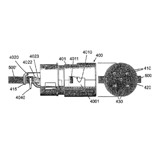
Fig. 4 to 7 show further embodiments of an assembly consisting of plug con-
nector 400 and circuit board 500 according to the invention, with Fig. 7 di-
vided into two separate drawings Fig. 7a, Fig. 7b. Fig. 7a shows the arrange-
ment of the contact elements outside the plane of the circuit board, that is
above and below the plane of the circuit board and Fig. 7b shows the ar-
rangement of the contact elements on the plane of the circuit board. The divi-
= CA 02835296 2013-11-07
,
9
sion has only been selected to provide a better overview. In this case the
plug
connector 400 is round in shape, with the housing 401 made of plastic. Con-
tact elements are arranged on the three planes in the plug connector 400 it-
self. A first plane above a circuit board 500 is provided with contact
elements
410. A contact element 420 is arranged at the level of the circuit board 500
and further contact elements 430 are arranged below plane of the circuit
board 500. The contact elements 410 arranged above the plane of the circuit
board are bent at right angles to the circuit board 500 and have contact ele-
ment ends 415. The contact elements 430 arranged below the planes of the
circuit board are angled at approximately 135 with respect to the circuit
board 500 and have contact element ends 435. The central contact element
420 extends linearly without bending and has a contact element 425. This
central contact element 420 extends into an opening 520 in the circuit board
500 in the form of an elongated hole with an entry opening 524 with a larger
cross-section than the contact area 522. Similarly, the openings 530 for the
1350 angled contact element ends 435 are also developed as elongated hole-
like openings with an entry area 534 that has a larger cross-section then the
contact area 532 accordingly. The openings 510 for the contact elements
bent at right angles are for example plated-through boreholes.
Inclined surfaces 441, 442 are arranged in the housing 401 of the plug con-
nector 400, these surfaces guiding and supporting the contact element ends
435 that extend obliquely. Similarly, the bent, right-angled contact elements
410 can also run along in corresponding housing sections 407, 405 (Fig. 4b).
Fig. 5a and 5b show isometric views of a plug connector, with the same ele-
ments as those in Figures 4a and 4b having the same reference symbols as
in those drawings. In contrast to the plug connectors illustrated
schematically
in Fig. 4a and Fig 4b, the plug connector shown in Fig. 5a and 5b is provided
on its outer perimeter and in the rear area facing the circuit board 500 with
shielding 490, that encompasses the housing 401 of the plug connector in an
annular fashion and encompasses resilient contact blades 491 bent outwards,
which for example are used in a metal housing to create an electrically con-
CA 02835296 2013-11-07
=
ductive connection (not shown), as well as the blades 492 bent inwards that
latch into the plug connector housing such that the shielding can be fastened
to the housing 401 in this way.
Furthermore, the shielding is provided with at least one wedge-shaped re-
bate, into which a corresponding rib 409 of the plug connector engages. This
prevents the pipe from rotating if torque is conducted into the plug housing
via
the inserted cable plug.
The arrangement of the contact elements on both sides of the circuit boards
200, 500 and therefore the arrangement of the central axis of the plug con-
nector on the same plane as the central axis of the circuit board, results in
an
even distribution of the forces generated during for example the plugging in
the process. The distribution of forces is considerably better than for a plug
connector that is only arranged on one side of the circuit board. As that type
of plug connector is arranged on one side of a circuit board outside the plane
of the circuit board, a certain plug connector "top heaviness" occurs as its
centre of gravity lies outside the circuit board. To counteract this top heavi-
ness, provision is made for openings 4001 in the housing 400 of the plug
connector according to the invention, with its one boundary surface 4010 fac-
ing the circuit board 500 having steps 4011, 4012, 4013 for adapting to differ-
ent circuit board thicknesses. This is shown schematically in Figure 5c to 5e,
where the arrangement of the plug connector is shown schematically on cir-
cuit boards of differing thicknesses 500', 500" and 500". The boundary sur-
face 4010 is provided with three steps 4011, 4012, 4013 in this embodiment,
with the step 4011 lying on a circuit board 500' with a thickness of for
example
2.0 measurement units, whereas the stepped surface 4012 lies on a circuit
board 500" with a thickness of 1.6 measurement units and the stepped sur-
face 4013 lies on a circuit board 500" with a thickness of 1.0 measurement
units. In order to make provision for a particularly good bearing for the plug
connector housing 400 on the circuit boards 500', 500", 500-, provision is
made additionally for a housing projection 4020 at the rear end of the housing
400 respectively facing the circuit board, with this projection also having a
CA 02835296 2013-11-07
11
stepped boundary surface facing the circuit board 500, 500", 500. The first
step 4021 forms a bearing surface that lies on the circuit board 500' with a
thickness of 2.0 measurement units. This step corresponds to the step 4011
of the collateral opening 4001 of the plug housing. Similarly, the bearing sur-
face formed by the step 4022 corresponds with the bearing surface 4012 of
the opening 4001 and the bearing surface formed by the step 4023 corre-
sponds with the bearing surface 4013 of the opening 4001. In this manner,
provision can be made for one and the same plug connector for mounting on
circuit boards of differing thicknesses, with it located on the circuit boards
with
no risk of turning over due to these bearing surfaces, which means that the
fabrication process (loading and soldering) is simplified immensely as one
can dispense with additional holding devices during the fabrication process
accordingly.
Fig. 8 schematically shows another embodiment of an assembly according to
the invention, where the plug connector 800 has a plurality of levels of con-
tacts 805 located above and adjacent to each other. Through-plated openings
810 are arranged in a circuit board 801 for these contact elements, as are
elongated openings 830 for linearly extending contact elements that are ter-
minated by through-plated boreholes at their ends, as well as elongated
openings 840, 850 that are also terminated at their ends for example by
through-plated boreholes 841, 851. However, in contrast to the embodiments
described above, some of the contact elements on the plane of the circuit
board are also bent, i.e. not bent towards the plane of the circuit board
below
and above the plane of the circuit board, but bent in the plane of the circuit
board itself, such as shown for example by the bends 8051 and 8052 of the
contact elements 805 lying on the plane of the circuit board. Provision can
also be made for the contact elements to be bent at the same time not only
on the plane of the circuit board, but also perpendicular to the plane of the
circuit board, such as for example the bend 8053 of the contact elements 805.
In any case the bends are developed to ensure that the contact elements are
CA 02835296 2013-11-07
,
,
12
arranged as optimally as possible on the circuit board, even for circuit
boards
of different thicknesses.
A particular advantage of such plug connectors is that they can be mounted
on circuit boards of differing thicknesses. The plugs are not bound to a fixed
circuit board thickness.
In a certain sense, the plug connector is "insensitive" to tolerances
involving
the thickness of the circuit board as a result of the bent contact elements on
both sides of the circuit board. Furthermore, it can be adapted to different
cir-
cuit board thicknesses easily. A further advantage is that such a plug connec-
tor can be made in a simple manner, particularly as the bent contact elements
can be produced in a simple manner.