Note: Descriptions are shown in the official language in which they were submitted.
CA 02835502 2013-11-08
WO 2012/152949
PCT/EP2012/058938
- 1 -
ION DETECTION
Technical Field of the Invention
The present invention concerns ion detection for a mass
analyser in which ions are caused to form ion packets that
oscillate with a period, including a ion detector and a
method of ion detection. Such a mass analyser may include an
Fourier Transform Ion Cyclotron Resonance (FTICR) mass
analyser, an electrostatic orbital trapping mass analyser or
any other ion trap with image current detection.
Background to the Invention
For Fourier Transform Mass Spectrometry (FTMS), the
detection limit of mass-to-charge (m/z) ratio analysis has
been defined in Marshall, A.G., Hendrickson C.L., "Fourier
Transform Ion Cyclotron Resonance Detection: Principles and
Experimental Configurations", Int. J. Mass Spectrom. 2002,
215, 59-75. There, the detection limit is considered the
minimum number of ions, M, of charge q detected with signal-
to-noise ratio 3:1. This detection limit has been shown as
proportional to the voltage noise of an input transistor of
the pre-amplifier (V,), the capacitance of the detection
circuit (Cdet) and inversely proportional to the relative
amplitude of detected oscillations, A. In other words,
Cdet Vn
M =const
qA
The voltage noise is determined by the process of
semiconductor manufacturing and improvement here is limited.
Also, the relative amplitude of detected oscillations is
limited by the quality of the trapping field and improvement
here is also difficult (for example, in practical
electrostatic orbital trapping analyzers, A is close to 60-
CA 02835502 2016-05-20
20086-2410
- 2 -
70%). Therefore, an improvement to the detection limit is
likely to be achieved by reducing the capacitance of the
detection circuit, Cdet.
WO-2008/103970 shows a wideband pre-amplifier for FTMS.
However, in this design, it is suggested that the signal-to-
noise ratio is optimised when the input capacitance of the JFET
transistor in the pre-amplifier is equal to the sum of the
wiring capacitance and the capacitance of the detection plate.
This is a different approach than the reduction in capacitance
suggested above.
Reduction of the parasitic capacitance in mass analysers is
typically implemented via passive measures, for instance by
separating detection electrodes, reducing their size or making
wires as short and thin as possible. All these methods provide
only an incremental improvement. It is desirable to provide a
significant reduction of multiple sources of capacitance using
another method.
Summary of the Invention
According to an aspect of the present invention, there is
provided an ion detector for a mass analyser in which ions are
caused to form ion packets that oscillate with a period, the
ion detector comprising: a detection arrangement, comprising: a
plurality of detection electrodes configured to detect a
plurality of image current signals from ions in the mass
analyser; and a preamplifier, wherein the preamplifier is
arranged to provide an output signal based on the plurality of
detected image current signals, the output signal having a
signal-to-noise ratio; and compensation circuitry, arranged to
CA 2835502 2017-05-31
81775361
- 2a -
provide at least one compensation signal, each compensation
signal being provided to a respective shielding conductor of
the detection arrangement and being based on one or more of the
plurality of detected image current signals; and wherein there
is a capacitance between each of the shielding conductors of
the detection arrangement and a respective signal-carrying part
of the detection arrangement, affecting the signal-to-noise
ratio of the preamplifier output signal, the compensatory
circuitry being arranged to cause a reduction in each
capacitance and an improvement in the signal-to-noise ratio
thereby.
According to another aspect of the present invention, there
is provided a method of ion detection for a mass analyser in
which ions are caused to form ion packets that oscillate with a
period, the method comprising: detecting a plurality of image
current signals using a plurality of detection electrodes that
form part of a detection arrangement, the detection arrangement
further comprising a preamplifier, wherein the preamplifier is
arranged to provide an output signal based on the plurality of
detected image current signals, the output signal having a
signal-to-noise ratio; providing at least one compensation
signal, each compensation signal being provided to a respective
shielding conductor of the detection arrangement and being
based on one or more of the plurality of detected image current
signals; and wherein there is a capacitance between each of the
shielding conductors of the detection arrangement and a
respective signal-carrying part of the detection arrangement,
affecting the signal-to-noise ratio of the preamplifier output
signal, and wherein the providing each compensation signal
CA 2835502 2017-05-31
81775361
- 2b -
causes a reduction in each capacitance and an improvement in
the signal-to-noise ratio thereby.
According to another aspect, there is provided an ion
detector for a mass analyser in which ions are caused to form
ion packets that oscillate with a period. The ion detector
comprises: a detection arrangement, comprising: a plurality of
detection electrodes configured to detect a plurality of image
current signals from ions in the mass analyser; and a
preamplifier, wherein the preamplifier is arranged to provide
an output signal based on the plurality of detected image
current signals, the output signal having a signal-to-noise
ratio; and compensation circuitry, arranged to provide at least
one compensation signal, each compensation signal being
provided to a respective compensatory part of the detection
arrangement and being
CA 02835502 2016-05-20
20086-2410
- 3 -
based on one or more of the plurality of detected image
current signals. There is a capacitance between each of the
compensatory parts of the detection arrangement and a
respective signal-carrying part of the detection
arrangement, affecting the signal-to-noise ratio of the
preamplifier output signal.
The compensation circuitry thereby causes a reduction
in the capacitance between each compensatory part of the
detection arrangement and its respective signal carrying
part of the detection arrangement. This reduction is from
the value that it would otherwise be were the compensation
circuitry not present.
In other words, the capacitance between each of the
compensatory parts of the detection arrangement and the
respective signal-carrying part of the detection arrangement
is defined when the compensation signal is not applied.
However, when each compensation signal is applied, it
compensates for the respective capacitance of the detection
arrangement, affecting the signal-to-noise ratio of the
preamplifier output signal. The capacitance between each of
the compensatory parts of the detection arrangement and the
respective signal-carrying part of the detection arrangement
when the compensation signal is applied is reduced in
comparison with the capacitance when the compensation signal
is not applied. In fact, between a compensatory parts of the
detection arrangement and a signal-carrying part of the
detection arrangement when the compensation signal is
applied may be effectively or substantially zero.
Advantageously, the compensation signal applied to the
compensatory part of the detection arrangement is based on a
signal carried by the respective signal-carrying part of the
detection arrangement- In some embodiments, the difference in signal
CA 02835502 2016-05-20
20086-2410
- 4 -
amplitude between the ac part of the compensation signal and
the ac part of the signal carried by the respective signal-
carrying part is relatively small in comparison with the
signal amplitude of the ac part of the signal carried by the
respective signal-carrying part. Optionally, the difference
in signal amplitude of the ac part is no more than 10%, 5%,
2.5%, 1% or 0.5%. Beneficially, the difference in phase
between the compensation signal and the signal carried by
the respective signal-carrying part is small. Optionally,
the difference in phase is less than 90 degrees, 45 degrees,
30 degrees, 15 degrees, 10 degrees, 5 degrees or 1 degree.
In one embodiment, the signal-carrying part of the
detection arrangement comprises a detection electrode from
the plurality of detection electrodes and the respective
compensatory part of the detection arrangement comprises a
shield for the detection electrode. The respective
compensation signal may be provided to the shield to cause
effectively zero capacitance between the shield and the
detection electrode. Here, the shield may be adjacent to the
detection electrode. In some embodiments, the shield for the
detection electrode comprises a conductive surface around
the detection electrode, insulated from the detection
electrode. In some embodiments, the shield for the detection
electrode is made from a dielectric material, preferably
glass, with metallised outer and inner coatings, the
metallised inner coating being configured to detect the ion
signal and the metallised outer coating being configured to
receive the compensation signal. This arrangement is
particularly advantageous for electrostatic orbital
trapping-type mass analysers, for example of the type
described in US 5,886,346 and available under the trade name
Orbitrap.
CA 02835502 2016-05-20
20086-2410
- 5 -
Additionally or alternatively, a signal-carrying part
of the detection arrangement may comprise a connection, such
as a wire, between a detection electrode from the plurality
of detection electrodes and the preamplifier and the
respective compensatory part of the detection arrangement
may comprise a shield for the connection. The respective
compensation signal may be provided to the shield to cause
effectively zero capacitance between the shield and the
connection. The shield for the detection electrode and the
shield for the connection may be electrically connected.
Then, a single common compensation signal may be provided to
both the shield for the detection electrode and shield for
the connection.
In some embodiments, the preamplifier comprises
a first voltage buffer arranged to receive a first image
current signal from the plurality of image current signals.
In such an embodiment, the compensation circuitry may be
arranged to provide a first compensation signal, comprising
an output of the first voltage buffer. In this way, the
first compensation signal is based on the first image
current signal. The first voltage buffer may provide a low
output impedance. In some embodiments, the first voltage
buffer comprises a transistor, for example a low-noise JFET
with the lowest possible gate capacitance and the highest
possible transconductance..
In some embodiments, the compensation circuitry is
further arranged to provide a second compensation signal,
based on a second image current signal from the plurality of
detected image current signals. The second compensation
signal may be provided to a second compensatory part of the
detection arrangement, there being a capacitance between the
second compensatory part of the detection arrangement and a
CA 02835502 2016-05-20
20086-2410
- 6 -
respective, second signal-carrying part of the detection
arrangement affecting the signal-to-noise ratio of the
preamplifier output signal. Here, the preamplifier may
further comprise a second voltage buffer, arranged to
receive the second image current signal, the second
compensation signal comprising an output of the second
voltage buffer. Again, the second voltage buffer may provide
a low output impedance. In some embodiments, the second voltage buffer
comprises a transistor, and beneficially may comprise a low-noise
JFET with the lowest possible gate capacitance and the
highest possible transconductance. Optionally for this
arrangement, the first signal-carrying part of the detection
arrangement comprises a first detection electrode, the
respective compensatory part comprising a first shield for
the first detection electrode. This reduces the capacitance
between the first detection electrode and ground. Also, the
second signal-carrying part may comprise a second detection
electrode, the respective compensatory part comprising a
second shield for the second detection electrode. This
reduces the capacitance between the second detection
electrode and ground.
Optionally, the first voltage buffer may comprise a
transistor in a common drain configuration. Then, the
compensation circuitry may be further arranged to provide a
drain compensation signal to the drain of the transistor.
This may reduce the effective capacitance between the gate
and drain of the transistor. In some cases, the compensation
circuitry is arranged to provide a second compensation
signal to a second compensatory part of the detection
arrangement and the preamplifier comprises a second voltage
buffer, arranged to receive the second image current signal,
the second compensation signal comprising an output of the
CA 02835502 2016-05-20
20086-2410
- 7 -
second voltage buffer. In such cases, the preamplifier may
further comprise a differential amplifier arranged to
receive the output of the first voltage buffer and the
output of the second voltage buffer and to provide a
differential output, the differential amplifier, in some embodiments,
being further configured to provide the drain compensation
signal. Optionally, the drain compensation signal is based
on the second image current signal, especially in the case
of symmetrical differential input signals.
Optionally, the compensation signal could be provided
in a more conventional way, that is using a cascade
configuration of the input buffer. This means that an
additional transistor in the input buffer is connected in
series in common base (or gate) configuration with the drain
of the input follower, wherein base (or gate) of the common
base (or gate) transistor is DC-coupled or AC-coupled to the
output of the input buffer. Therefore, this may make the use
of the second signal output unnecessary for providing a
compensation signal.
In some embodiments, the differential amplifier comprises a
first amplifier transistor arranged to receive the output of
the first voltage buffer and a second amplifier transistor
arranged to receive the output of the second voltage buffer,
the first and second amplifier transistors being arranged as
a differential pair. The drain compensation signal may be
provided from a signal at the drain of the second amplifier
transistor. Optionally, the drain compensation signal is a
first drain compensation signal provided to the drain of the
transistor of the first voltage buffer and the second
voltage buffer may comprise a transistor in a common drain
configuration. Then, the at least one compensation signal
may further comprise a second drain compensation signal
CA 02835502 2016-05-20
20086-2410
- 8 -
provided to the drain of the transistor of the second
voltage buffer, the second drain compensation signal being
provided from a signal at the drain of the first amplifier
transistor. This may reduce the capacitance between the gate
and drain of the transistor.
In some embodiments, the compensation circuitry
is arranged to provide a first shield compensation signal to
a first shield compensatory part of the detection
arrangement and a second shield compensation signal to a
second shield compensatory part of the detection
arrangement. Then, the first shield compensation signal and
the second shield compensation signal may be the same.
Optionally, the first shield compensatory part may comprise
a shield for a first detection electrode from the plurality
of detection electrodes and the second shield compensatory
part may comprise a shield for a connection between the
first detection electrode and the preamplifier.
Alternatively, the first shield compensatory part may
comprise a shield for a second detection electrode from the
plurality of detection electrodes and the second shield
compensatory part may comprise a shield for a connection
between the second detection electrode and the preamplifier.
Advantageously, compensation signals for the shield for the
first detection electrode, the shield for the second
detection electrode, the shield for a connection between the
first detection electrode and the preamplifier and the
shield for a connection between the second detection
electrode and the preamplifier are provided.
A further advantageous feature of the ion detector of some
embodiments may be a shielding conductor, positioned between a first
detection electrode and a second detection electrode from
the plurality of detection electrodes and configured to be
CA 02835502 2013-11-08
WO 2012/152949 PCT/EP2012/058938
- 9 -
c onne ct ed to a voltage source, which is preferably external.
The voltage source optionally provides a fixed voltage. This
reduces the capacitance between the first detection
electrode and the second detection electrode. Optionally,
the voltage source is configured to provide a voltage to the
shielding conductor based on the image current detected by
at least one of the plurality of detection electrodes so as
to compensate for a change in frequency of oscillation for
ions confined in the ion trapping volume caused by space
charge.
Beneficially, the pre-amplifier may comprise a
differential amplifier comprising a plurality of amplifier
transistor pairs. Here, each amplifier transistor pair may
comprise: a respective first amplifier transistor arranged
to receive a signal based on a first image current signal;
and a respective second amplifier transistor arranged to
receive a signal based on a second image current signal.
Then, the respective first and second amplifier transistor
of each amplifier transistor pair may be arranged as a
differential pair and the plurality of amplifier transistor
pairs may be arranged in parallel. This reduces the overall
power spectral density of noise generated by the plurality
of amplifier transistor pairs in comparison with the case
where only one amplifier transistor pair is used.
The present invention also provides a mass spectrometer
comprising a mass analyser and the ion detector as described
herein.
There is provided, in an associated aspect of the
present invention a method of ion detection for a mass
analyser in which ions are caused to form ion packets that
oscillate with a period. The method comprises: detecting a
plurality of image current signals using a plurality of
CA 02835502 2013-11-08
WO 2012/152949 PCT/EP2012/058938
- 10 -
detection electrodes that form part of a detection
arrangement, the detection arrangement further comprising a
preamplifier, wherein the preamplifier is arranged to
provide an output signal based on the plurality of detected
image current signals, the output signal haying a signal-to-
noise ratio; and providing at least one compensation signal,
each compensation signal being provided to a respective
compensatory part of the detection arrangement and being
based on one or more of the plurality of detected image
current signals. There is a capacitance between each of the
compensatory parts of the detection arrangement and a
respective signal-carrying part of the detection
arrangement, affecting the signal-to-noise ratio of the
preamplifier output signal.
Alternatively, a method of ion detection for a mass
analyser in which ions are caused to form ion packets that
oscillate with a period can be described. The method
comprises: detecting a plurality of image current signals
using a plurality of detection electrodes that form part of
a detection arrangement, the detection arrangement further
comprising a preamplifier, wherein the preamplifier is
arranged to provide an output signal based on the plurality
of detected image current signals, the output signal having
a signal-to-noise ratio; and providing at least one
compensation signal, each compensation signal being provided
to a respective compensatory part of the detection
arrangement to compensate for a respective capacitance of
the detection arrangement, affecting the signal-to-noise
ratio of the preamplifier output signal. Preferably, each
compensation signal is based on one or more of the plurality
of detected image current signals.
CA 02835502 2016-05-20
20086-2410
- 11 -
In some embodiments, a signal-carrying part of the detection
arrangement comprises a detection electrode from the
plurality of detection electrodes and the respective
compensatory part of the detection arrangement comprises a
shield for the detection electrode. In some embodiments, the
shield for the detection electrode comprises a conductive
surface around the detection electrode, insulated from the
detection electrode.
Additionally or alternatively, a signal-carrying part
of the detection arrangement comprises a connection between
a detection electrode from the plurality of detection
electrodes and the preamplifier and the respective
compensatory part of the detection arrangement comprises a
shield for the connection.
In some embodiments, the preamplifier comprises a first
transistor voltage buffer arranged to receive a first image
current signal from the plurality of image current signals
and the at least one compensation signal comprises a first
compensation signal, comprising an output of the first
transistor voltage buffer. In this way, the first
compensation signal is based on the first image current
signal. Optionally, the at least one compensation signal
further comprises a second compensation signal, based on a
second image current signal from the plurality of detected
image current signals, the second compensation signal being
provided to a second compensatory part of the detection
arrangement, there being a capacitance between the second
compensatory part of the detection arrangement and a
respective, second signal-carrying part of the detection
arrangement affecting the signal-to-noise ratio of the
preamplifier output signal. Then, the preamplifier may
further comprise a second transistor voltage buffer,
CA 02835502 2016-05-20
20086-2410
- 12 -
arranged to receive the second image current signal, the
second compensation signal comprising an output of the
second transistor voltage buffer. In one embodiment, a first
signal-carrying part of the detection arrangement comprises
a first detection electrode, the respective compensatory
part comprising a first shield for the first detection
electrode and the second signal-carrying part comprises a
second detection electrode, the respective compensatory part
comprising a second shield for the second detection
electrode.
In some embodiments, the first voltage buffer comprises
a transistor in a common drain configuration and wherein the
at least one compensation signal further comprises a drain
compensation signal provided to the drain of the transistor.
Then, the method optionally further comprises:
receiving the output of the first transistor voltage buffer
and the output of the second transistor voltage buffer at a
differential amplifier in the pre-amplifier; and providing a
differential output from the differential amplifier. Then,
the step of providing at least one compensation signal may
comprise providing the drain compensation signal from the
differential amplifier. Here, the drain compensation signal
may be based on the second image current signal.
In some embodiments, the differential anpdifier comprises a
first amplifier transistor arranged to receive the output of
the first transistor voltage buffer and a second amplifier
transistor arranged to receive the output of the second
transistor voltage buffer, the first and second amplifier
transistors being arranged as a differential pair.
In some embodiments, the drain compensation signal is provided from a
signal at the drain of the second amplifier transistor.
Optionally, the drain compensation signal is a first drain
CA 02835502 2016-05-20
20086-2410
- 13 -
compensation signal, the second voltage buffer comprising a
transistor in a common drain configuration and the at least
one compensation signal further comprises a second drain
compensation signal provided to the drain of the transistor
of the second voltage buffer. Then, the second drain
compensation signal may be provided from a signal at the
drain of the first amplifier transistor. This may reduce the
capacitance between the gate and drain of the transistor.
In some embodiments, the at least one compensation
signal comprises: a first shield compensation signal
provided to a first shield compensatory part of the
detection arrangement; and a second shield compensation
signal provided to a second shield compensatory part of the
detection arrangement. Then, the first shield compensation
signal and the second shield compensation signal are
preferably the same. The first shield compensatory part may
comprise a shield for a first detection electrode from the
plurality of detection electrodes and the second shield
compensatory part may comprise a shield for a connection
between the first detection electrode and the preamplifier.
In some embodiments, the method further
comprises providing a shielding conductor coupled to a
voltage positioned between a first detection electrode and a
second detection electrode from the plurality of detection
electrodes.
Also in some embodiments, the pre-amplifier may
comprise a differential amplifier comprising a plurality of
amplifier transistor pairs, each amplifier transistor pair
comprising: a respective first amplifier transistor arranged
to receive a signal based on a first image current signal;
and a respective second amplifier transistor arranged to
receive a signal based on a second image current signal, the
= 81775361 CA 2835502 2017-05-31
- 14 -
respective first and second amplifier transistor of each
amplifier transistor pair being arranged as a differential
pair and wherein the plurality of amplifier transistor pairs
are arranged in parallel.
In another aspect, there is provided an
electrostatic ion trapping device comprising: a trapping
field generator, configured to provide a trapping'field
defining an ion trapping volume, in which ions are confined; a
detection arrangement, configured to detect an image current
from ions trapped in the ion trapping volume, using a
plurality of detection electrodes; a shielding conductor,
= positioned between a first detection electrode and a second
detection electrode from the plurality of detection
electrodes; and a controller, configured to apply a voltage
to the shielding conductor based on an image current
detected by at least one of the plurality of detection
electrodes.
This electrostatic ion trapping device (optionally, an
electrostatic orbital trapping-type device) advantageously
comprises a shielding conductor between a first detection
electrode and a second detection electrode, which reduces
the capacitance between these two electrodes.
In some embodiments, the ion trapping device defines an axis and
the shielding conductor is between the first and second detection
electrodes along this axis. In some embodiments, the trapping
field generator is configured to confine ions so as to cause
the ions to oscillate along the axis. The axis is optionally
longitudinal. Beneficially, the controller is configured to
apply an AC voltage to the shielding conductor.
Moreover, the shielding conductor provides a different
benefit from the compensation circuitry described above. At
large ion numbers, the oscillation frequency of the ions
CA 02835502 2016-05-20
20086-2410
- 15 -
shifts, due largely to image charges induced in all
electrodes by moving ions. By modulating the voltage induced
an electrode in-phase or out of phase with the detected
image current signal, this effect is cancelled out,
improving mass accuracy and dynamic range of analysis.
Advantageously, in some embodiments, the controller is configured
to apply the voltage to the shielding conductor based on the image
current detected by at least one of the plurality of
detection electrodes so as to compensate for a change in
frequency of oscillation for ions confined in the ion
trapping volume caused by space charge. It may be understood
that the ion trapping volume defines the axis and that the
frequency of oscillation relates to axial oscillation.
Optionally, the trapping field generator comprises an
inner electrode arranged along the axis and the
electrostatic ion trapping device further comprises first
and second outer electrodes, positioned along the axis
concentric with the inner electrode to enclose the inner
electrode and to define a space between the inner electrode
and outer electrodes, said space defining the ion trapping
volume. In embodiments, the plurality of detection
electrodes comprise one or more of: the inner electrode; the
first outer electrode; and the second outer electrode.
In some embodiments, the first detection electrode is the first
outer electrode and the second detection electrode is the
second outer electrode. Alternatively, one of the detection
electrodes may comprise the inner electrode. Also, more than
one inner electrode can optionally be provided. In some such
cases, the first detection electrode may be a first inner
electrode. Optionally, the second detection electrode may be
a second inner electrode.
CA 02835502 2016-05-20
20086-2410
- 16 -
In some embodiments, the shielding conductor comprises
a ring concentric with the inner electrode. Additionally or
alternatively, the shielding conductor may comprise a
segment formed at a central part (along the axis) of the
inner electrode.
In some embodiments, the shielding conductor is located to avoid
significant coupling of AC signal from the detection
electrodes. This avoids too great an attractive force
towards the shielding conductor.
In a further aspect, there is provided a method of
electrostatic ion trapping comprising: causing ions to be
trapped in an ion trapping volume; and detecting an image
current from ions trapped in the ion trapping volume using a
plurality of detection electrodes; providing a shielding
conductor, positioned between a first detection electrode
and a second detection electrode from the plurality of
detection electrodes; and applying a voltage to the
shielding conductor based on an image current detected by at
least one of the plurality of detection electrodes. This
method can optionally further comprise additional features
to mirror those defined in respect of the corresponding
electrostatic ion trapping device defined herein.
It will also be understood that the present invention
is not limited to the specific combinations of features
explicitly disclosed, but also any combination of features
that are described independently and which the skilled
person could implement together.
Brief Description of the Drawings
The invention may be put into practice in various ways,
one of which will now be described by way of example only
and with reference to the accompanying drawings in which:
CA 02835502 2013-11-08
WO 2012/152949
PCT/EP2012/058938
- 17 -
Figure 1 shows a schematic arrangement of an existing
mass spectrometer including an electrostatic trap mass
analyser and an external storage device;
Figure 2 shows the existing electrostatic trap mass
analyser of Figure 1 in more detail, together with existing
detection circuitry;
Figure 3 illustrates a first embodiment of an ion
detection arrangement according to the present invention;
Figure 4 shows a schematic illustration of the ion
detection arrangement embodiment shown in Figure 3 with
additional details;
Figure 5 illustrates a second embodiment of a pre-
amplifier according to the present invention for use with
the ion detection arrangement of Figure 4;
Figure 6 depicts an electrostatic trap mass analyzer
according to a third embodiment of the present invention;
Figure 7 shows a third embodiment of a pre-amplifier
according to the present invention for use with the ion
detection arrangement of Figure 4;
Figure 8 illustrates an ion detection arrangement
incorporating the electrostatic trap mass analyzer of Figure
6 and the third embodiment of the pre-amplifier of Figure 7;
Figure 9 illustrates variants of design solutions for
the differential input stage of Figures 7 and 8.
Detailed Description of Preferred Embodiments
Referring first to Figure 1, a schematic arrangement of
an existing mass spectrometer including an electrostatic
trap and an external storage device is shown. The
arrangement of Figure 1 is described in detail in commonly
assigned WO-A-02/078046 and WO-A-2006/129109 and will not be
described in detail here. More details regarding this
CA 02835502 2016-05-20
20086-2410
- 18 -
arrangement can be found in these two documents.
Figure 1 is included in order better to understand the
use and purpose of the electrostatic trap mass analyser.
Although the present invention is described in relation to
such an electrostatic trap mass analyser, it will be
appreciated that it can also be applied to other kinds of
electrostatic trap mass analyser, employing image current
detection or an electrostatic field causing ions to form ion
packets that oscillate with a period, such as a Fourier
Transform Ion Cyclotron Resonance (FTICR) mass analyser.
As seen in Figure 1, the mass spectrometer 10
comprises: a continuous or pulsed ion source 20; an ion
source block 30; an RF transmission device 40 for cooling
ions; a linear ion trap mass filter 50; a transfer octapole
device 55; a curved linear trap 60 for storing ions; a
deflection lens arrangement 70; the electrostatic trap 75,
which is the electrostatic orbital trapping-type of mass
analyser (as sold by Thermo Fisher Scientific under the
trade name Orbitrap) comprising a split outer electrode
(comprising first electrode 80 and second electrode 85) and
an inner electrode 90. There may also be an optional
secondary electron multiplier (not shown), on the optical
axis of the ion beam.
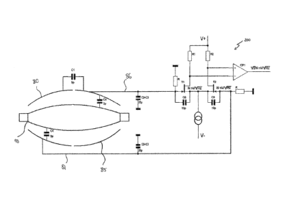
Referring now to Figure 2, there is shown the existing
electrostatic trap mass analyser of Figure 1 in more detail,
together with existing detection circuitry. An image current
is detected using a differential amplifier on the first
outer electrode 80 and second outer electrode 85 of the trap
as shown on Figure 2. The first outer electrode 80 and
second outer electrode 85 are referred to as detection
electrodes. First 'conductor 81 and second conductor 86 carry
CA 02835502 2013-11-08
WO 2012/152949 PCT/EP2012/058938
- 19 -
a first image current signal and a second image current
signal respectively to pre-amplifier 200.
The pre-amplifier 200 comprises: a first amplifier
transistor T2; and a second amplifier transistor Tl; first
resistor R1; second resistor R2; and an operational
amplifier OP1. The first amplifier transistor T2 and the
second amplifier transistor T1 are connected as a
differential pair, together with first resistor R1 and
second resistor R2 and a constant current source forming a
differential amplifier.
Figure 2 also schematically depicts a variety of
partial, parasitic capacitances, the interaction of which
causes an overall capacitance for the detection circuit.
Some parasitic resistances are also shown for completeness.
The overall capacitance for the detection circuit, 0dõ, is a
combination of the following partial capacitances (typical
values for a standard electrostatic orbital trapping
analyzer are presented in brackets):
1. capacitance between first outer electrode 80 and second
outer electrode 85 (C1=5 pF, estimated);
2. capacitance between each detection electrode and ground
(C2=20 pF);
3. capacitance between conductors (wires) leading from
each detection electrode to the pre-amplifier and
ground (C3=5 pF);
4. capacitance between each detection electrode and the
central electrode 90 (C4=3 pF);
5. capacitance between each detection electrode to other
electrodes, for example to deflection lens arrangement
70 (C5=3 pF); and
6. gate-drain capacitance of the first input transistor T2
of the pre-amplifier and gate-drain capacitance of the
CA 02835502 2013-11-08
WO 2012/152949 PCT/EP2012/058938
- 20 -
second input transistor T1 of the pre-amplifier (C6=10
pF).
For the exemplified capacitance values above, the
overall capacitance of the detection arrangement, including
the detector electrodes and pre-amplifier is given by
Cdet=C1+ 0.5*(C2+C3+C4+C5+C6).
Based on the typical, estimated values given above, Cdet
= 25.5 pF.
The first amplifier transistor T2 and second amplifier
transistor T1 are typically JFET transistors. A single JFET
transistor has a spectral noise density, N (normally
measured in nV/A/Hz) and a typical value is 0.85 nV/Nfliz. The
overall noise density of the differential input stage is
given by N'2*N. Thus, the signal-to-noise ratio (S/N) of the
arrangement shown in Figure 2 is proportional to
S/N oc 1/ (Cdet*1/2*N)
It will be appreciated that increasing the signal-to-
noise ratio by decreasing Cdct also results in an improvement
in the detection limit, M, identified above. If the signal-
to-noise ratio is increased by reducing Cdctr then
conversely, the number of ions needed to achieve the same
signal-to-noise ratio is reduced.
Referring next to Figure 3, a first embodiment of an
ion detection arrangement according to the present invention
is shown. The embodiment shown in Figure 3 is based on that
of Figure 2, but with a number of significant changes. This
embodiment exemplifies a way of detecting the image current
signals. Features that are the same as those shown in
CA 02835502 2013-11-08
WO 2012/152949
PCT/EP2012/058938
- 21 -
Figures 1 or 2 are identified by identical reference
numerals.
In this case, outer electrodes 80 and 85 are made
preferably from a clear or high-ohmic glass with a low
temperature expansion coefficient. It is metallised (that
is, metal coated) in such a way that the outer coating is
not connected to the inner coating forming electrodes 80 and
85 but forms a first conductive surface 100 and a second
conductive surface 105, each surrounding electrodes 80 and
85, correspondingly and thereby acting as shields. These
surfaces 100, 105 could have a gap between them or,
optionally, this gap could be covered by a high-ohmic
resistive layer 110 (total resistance preferably above 1
MOhm and more preferably above 10 MOhm). Preferably, these
surfaces also have a connection to the inner surface of the
glass form (not shown) and form a barrier between electrodes
80 and 85.
First conductor (wire) 81 and second conductor (wire)
86 from first detection electrode 80 and second detection
electrode 85 connect these electrodes to the first stage of
buffering or amplification formed by FET transistors 82 and
87 respectively. These wires are surrounded by first
conductive shield 101 and second conductive shield 106 which
are also electrically connected to conductive surfaces 100
and 105 respectively. However, the conductive shields 101
and 106 for the connections need not be electrically
connected to conductive surfaces 100 and 105 in cases where
the conductive surfaces 100 and 105 have their own
connections to the compensation signal.
As signals from electrodes 80 and 85 gets amplified by
FET transistors 82 and 87, they get de-coupled from the
incoming signals and could be used for differential
CA 02835502 2013-11-08
WO 2012/152949
PCT/EP2012/058938
- 22 -
amplification by amplifier 120, but also for active
compensation. For the latter, first repeater (buffer or
amplifier) 83 and second repeater (buffer or amplifier) 88
feed the signals back to shields 101 and 106 and conductive
surfaces 100 and 105. In this way, the total attenuation of
incoming signal is exactly (or close to) unity.
Thus, no voltage difference is formed between
electrodes 80, 85 and the corresponding conductive surfaces
(acting as shields) 100 and 105. This is because the
potential difference between the first electrode 80 and the
first conductive surface 100 is minimised, such that the
capacitance between them is effectively nullified. The same
applies to the second electrode 85 and the second conductive
surface 105. By extension, this also applies to first
conductor 81 and first shield 101 and second conductor 86
and second shield 106. This approach allows reduction in C2,
C3, C5 to substantially zero. In addition, C1 could be
decreased if a barrier between the first electrode 80 and
second electrode 85 is provided as described above.
WO-03/048789 provides some information on a general
capacitance compensation approach in some ways similar to
the compensation used here, as applied to electrodynamic
sensors for medical applications.
In practice, the finite response time of first FET 82,
second FET 87, first repeater 83 and second repeater 88
results in the appearance of a small phase shift between the
image current signals detected by the electrodes and the
active compensation signals. However, for the frequency
range typically of interest (200-2000 kHz), this phase shift
will be only a few degrees. This will not prevent a
reduction in C2, C3, C5 by at least a factor of 5 to 10.
CA 02835502 2013-11-08
WO 2012/152949 PCT/EP2012/058938
- 23 -
Referring next to Figure 4, there is shown a schematic
illustration of the embodiment shown in Figure 3 with
additional details. The parasitic capacitances and
resistances that were shown in Figure 2 are also shown in
this drawing. The capacitances between each of the detection
electrodes and ground and between the conductors (wires) and
ground (C2+C3) and the capacitance between input to the pre-
amplifier and ground (C6) now provide the greatest
contributions towards Cdet. In addition to the shields 100,
105 and 101, 106, further active shielding is implemented by
providing additional buffer amplifiers using a first buffer
transistor T4 as part of a first voltage follower 130 and a
second buffer transistor T3 as part of a second voltage
follower 135 (first buffer transistor T4 and second buffer
transistor T3 having the same noise spectral density, N).
The first voltage follower 130 drives first shield 101 and
first conductive surface 100 and the second voltage follower
135 drives the second shield 106 and the second conductive
surface 105.
This approach actually increases the overall noise
spectral density by factor of N'2, but the effective
capacitance value for the detection circuitry, CdeL, is
drastically reduced. By compensating for capacitances C2 and
C3 and decreasing capacitance C6 to about 1/5 of the
original value, the effective typical total capacitance
becomes
C - C1+ 0.5*(C2+C3+C4+C5+C6)
5 + 0.5*(0+0+3+0+2) = 7.5pF.
As noted above, the noise spectral density for the pre-
amplifier 120 is worsened by factor of -\j2, becoming equal to
2N nV/A/Hz. Nevertheless, the S/N for this circuit becomes
CA 02835502 2013-11-08
WO 2012/152949 PCT/EP2012/058938
- 24 -
S/N' -1/ (7.5*2*N) .
Comparing to 1/ (Cdet*112 *N) as given above for the
embodiment of Figure 2, an improvement of the S/N, G, is
approximately
G=(25.5*N12) / (7.5*2) =2.4.
Hence, the reduction in capacitance causes an
improvement in the S/N which is significantly greater than
the reduction in S/N due to the increase in noise power
spectral density of the pre-amplifier. However, further
improvements are also possible, particularly within the pre-
amplifier.
Referring now to Figure 5, there is shown a second
embodiment of a pre-amplifier according to the present
invention for use with the ion detection arrangement of
Figure 4. The pre-amplifier 300 is similar to the pre-
amplifier 120 shown in Figure 4. However, it also includes
additional features to compensate for the input capacitance
of the pre-amplifier.
A signal with the same amplitude and phase as the input
signal to the preamplifier from first detection electrode 80
is connected to the drain of the FET transistor T4 that is
part of the first voltage follower 130. Similarly, a signal
with the same amplitude and phase as the input signal to the
preamplifier from second detection electrode 85 is connected
to the drain of the FET transistor T3 that is part of the
second voltage follower 135. This means that all three
terminals of the transistor for each voltage follower have
the same AC voltage and virtually no input capacitance
between the terminals.
CA 02835502 2013-11-08
WO 2012/152949 PCT/EP2012/058938
- 25 -
This is achieved by taking the signal applied to the
drain of the FET transistor T4 of the first voltage follower
130 from the drain of the second amplifier transistor Tl
with an additional resistor, R4. Similarly, the signal
applied to the drain of the FET transistor T3 of the second
voltage follower 135 is taken from the drain of the first
amplifier transistor T2 with an additional resistor, R3. The
resistance values of R3 and R4 should be chosen from the
equation
R=2/Yfs.
where Yfs is the forward transfer admittance of a JFET
transistor. A typical value for Cdet is now reduced from
7.5 pF to 6.5 pF, since C6 is effectively reduced to
approximately zero. Then, the overall S/N improvement, G, in
this case becomes
G=(25.5*N12) / (6.5*2)= 2.77
The resistance values of R3 and R4 could be also chosen
to differ from the equation above. For example, they could
be chosen to over-compensate C6. However, over-compensation
of the entire total capacitance of the detection circuit is
not desirable, as it may lead to instability of the
preamplifier.
Further reductions in capacitance can be achieved by
means other than compensation. Referring next to Figure 6,
there is a shown an electrostatic trap mass analyzer
according to a third embodiment of the present invention.
This shows the electrostatic orbital trapping-type of the
mass analyzer shown in Figures 1 to 4, but with an
additional feature. A conductor, here formed as a metal ring
CA 02835502 2013-11-08
WO 2012/152949
PCT/EP2012/058938
- 26 -
140, is installed between the first detector electrode 80
and the second detector electrode 85. The gap between the
metal ring 140 to each of electrodes is the same and the
metal ring 140 is connected to voltage supply 145. The
voltage supply 145 is preferably external.
Typically, a few hundred volts are applied to the metal
ring 140 in order to get the field inside the mass analyser
correct. This voltage is desirably static during detection,
but could be switchable at other times. Preferably, this
voltage has a ripple below a few (1, 2 or 3) millivolts and
preferably within a frequency range below 100 to 200 kHz.
The voltage on the metal ring 140 is adjusted to provide
optimum performance of the instrument, for example minimum
transient decay for all m/z analysed.
This conductor splits the parasitic capacitance C1 into
two parts with the same value and allows reduction of that
capacitance by half. The voltage applied to this conductor,
preferably from an external source, could be used to adjust
ion frequencies as described in US-7,399,962 Fig. 11 or
US-7,714,283 Fig. 5. This metal ring electrode 140 is used
for fine optimisation of device performance, which is
preferably carried out during the calibration process for
different intensities of ions having different m/z ratios.
The criteria for optimisation is to provide a uniform decay
constant for ion transients of all intensities for a given
m/z as well as monotonous dependence of this decay constant
-1
on m/z (preferably (m/z)/2 ).
In this case, a typical value for CdeL is reduced to 4
pF the S/N is now proportional to
S/N" oc 1/(4*2*N).
CA 02835502 2013-11-08
WO 2012/152949 PCT/EP2012/058938
- 27 -
Then, the overall improvement in S/N becomes
G=(25.5*N12) / (4*2)= 4.5.
Referring next to Figure 7, there is shown a third
embodiment of a pre-amplifier according to the present
invention for use with the ion detection arrangement of
Figure 4. This pre-amplifier 310, includes all of the
features shown in the pre-amplifier 300 of Figure 5.
However, it now includes an additional feature to improve
further the S/N ratio. The first amplifier transistor T2 and
second amplifier transistor T1 are formed from a set of
transistors (normally substantially identical) connected in
parallel. Where K such transistors are provided (K being an
integer greater than 1), there are a plurality of first
amplifier transistors T2_1 to 12_K and a plurality of second
amplifier transistors T1_1 to T1 K.
This approach reduces overall spectral noise density of
the pre-amplifier by factor in the range 2N to Nr2N. For K
such pairs of transistors in parallel, the overall noise
spectral density of the Pre-amplifier with the buffer stage
become equal to N'[2 (1 +1/K)]"2.
In practice, there may be difficulties in driving more
then 3 or 4 paralleled transistors by a single voltage
buffer formed of a single JFET, because the input
capacitance of paralleled transistors becomes too high. The
table below provides estimates of the S/N improvement in
circuits with up to four transistors in each side of the
differential stage relative to the design shown in Figure 2.
The improvements shown in Figures 3 to 6 are also taken into
account.
CA 02835502 2013-11-08
WO 2012/152949 PCT/EP2012/058938
- 28 -
Transistor 1 2 3 4
count, K
Overall
noise
2N 1.73N 1.63N 1.58N
spectral
density
Overall S/N
4.5 5.2 5.5 5.7
improvement
All numbers shown in the table for overall S/N
improvements may be considered absolute upper limits for a
simplified analysis of the image current detection system.
In practice, the S/N improvement may be lower and depend on
the type of input transistors and the depth of capacitive
feedback created by the compensation signal at the input
buffer stage of the amplifier.
Referring now to Figure 8, there is shown an ion
detection arrangement incorporating the electrostatic trap
mass analyzer of Figure 6 and the third embodiment of the
pre-amplifier of Figure 7. Also shown are any remaining
parasitic capacitances and resistances for comparison with
those shown in Figure 2.
The parasitic capacitance C4 is determined by the
physical design of the electrostatic orbital trapping-type
mass analyzer. In principle, the parasitic capacitance C4
could be reduced in a similar way to the approach taken by
the embodiment shown in Figure 6, by splitting the central
electrode 90 in two and feeding active compensation to each
half via a decoupling high-voltage capacitance. This could
be undertaken independently from the other measures taken.
However, the gain from this measure is not likely to be
substantial and therefore does not justify a considerable
CA 02835502 2013-11-08
WO 2012/152949
PCT/EP2012/058938
- 29 -
increase in complexity and cost. Moreover, C4 represents the
smallest parasitic capacitance to affect the signal
intensity and the most difficult to compensate due to high
voltages applied to the central electrode 90 (which may
typically reach 5 kV).
Altogether, active compensation allows in principle to
reduce typical effective capacitance (Cdet) from about 24 pF
to about 5 or 6 pF, as explained above. In addition, the
compensation approach taken is expected to allow additional
freedom of design. For example: the walls of the mass
spectrometer chamber could come now much closer to the mass
analyser assembly; and the wires to the pre-amplifier could
be made longer (if necessary). Most importantly, the shields
101 and 106 and conductive surfaces 100 and 105 used for
active compensation are also shielding detection electrodes
80 and 85 from other sources of noise, especially from
ground loops. Further S/N improvement to that suggested
above may therefore be possible.
Referring next to Figure 9, there is shown variants of
design solutions for the differential input stage of Figures
7 and 8. The input differential stage shown could be any
known circuit that comprises some cascode combination of the
transistors or any other known circuit solutions providing
the same effect as shown in Figure 9.
Transistors on that stage could be any low noise types
like JFET, MOSFET or BJT npn/pnp. The Vbiõ voltage could be
a constant potential or a voltage that follows the input
common mode signal. Input buffer transistors T3 und T4 of
Figures 7 and 8 allow a reduction in the overall noise
density by using transistors with very low spectral noise
density. Normally such ultra-low noise transistors have
quite a large input capacitance, for example IF3601
CA 02835502 2013-11-08
WO 2012/152949
PCT/EP2012/058938
- 30 -
(manufactured by InterFet Corp.) has noise spectral density
of 0.3 nV/-\/Hz and 300 pF input capacitance and for the
IF9030, these figures are 0.5 nV/-\/Hz and 60pF.
The input buffer with a common drain (collector)
topology shown in Figures 7 and 8 cancels its input
capacitance and thus opens a possibility to drive paralleled
transistors with large input capacitance. This technique
could provide good improvement of the preamplifier noise
spectral density (up to factor of 2) compared with the
preamplifier employing a conventional low capacitance JFET
such as BF862 (manufactured by NXP Semiconductor with noise
spectral density of 0.8 nV/A/Hz and input capacitance of
10pF) in a differential stage without the input buffer.
Whilst specific embodiments have been described herein,
the skilled person may contemplate various modifications and
substitutions.
For example, this invention could be applied to all
types of FT-ICR instruments, RF ion traps and electrostatic
traps, including instruments with multiple detection
electrodes, for both odd and even numbers of such
electrodes.
This invention could be also used for active
compensation of effects related to space charge. For example
at large ion numbers, the oscillation frequency of the ions
shifts in any trap. This is to a large extent caused by the
image charges induced in all electrodes by moving ions. If
the voltage induced on some of the electrodes is modulated
in-phase or out of phase with the signal, this effect could
be cancelled out and traps could be made more tolerant to
high space charge. This in turn improves mass accuracy and
dynamic range of analysis.
CA 02835502 2013-11-08
WO 2012/152949 PCT/EP2012/058938
- 31 -
One of the ways to achieve this is to apply to the
metal ring 140 not only a compensating DC voltage but also
an AC signal. Preferably, the AC voltage is derived from
both detected signals, for example their difference scaled
with a certain coefficient. The DC voltage also could be
corrected dependent on the signal, such as to compensate for
change of frequency caused by space charge. This may improve
mass accuracy. Other electrodes could be used to the same
effect, including the detection electrodes themselves.
As an example, the DC voltage on all outer electrodes
could be biased by a voltage that compensates the drop of
the axial frequency caused by space charge. The expected
space charge could be estimated from the ion number
requested to be injected into the analyzer or directly from
the first milliseconds of the transient signal. The
compensation voltage could then be ramped slowly to the
required level so that the frequency shift over the entire
transient is nullified.
In another example, additional segments could be formed
near a central part of the central electrode so that ions
pass near these additional segments, but such that these
segments are too far from the detection electrodes to cause
significant coupling of an AC signal into the latter. If an
AC signal is formed from the detected signal and it is then
applied in-phase to these segments, this would cause
attraction of ions to the segments. By adjusting the
amplitude of the AC signal using an additional amplifier, it
would be possible to cause an attractive force that
completely compensates for the attraction from mirror
charges formed in the detection electrodes. As a result, the
frequency of oscillations will not depend on space charge,
CA 02835502 2013-11-08
WO 2012/152949
PCT/EP2012/058938
- 32 -
both overall for the entire beam and locally for a
particular m/z or limited m/z range.
The skilled person will appreciate that different types
of transistors can be used in conjunction with this
invention. Some transistors may have a lower noise level but
higher capacitance than other transistors. In such cases,
the total noise at the output of the preamplifier would
still be reduced when these transistors are used with this
invention. This is in view of the reduction in Cdet due to
other sources, as explained above.