Note: Descriptions are shown in the official language in which they were submitted.
CA 02835553 2013-11-08
= 1
PANE WITH AN ELECTRICAL CONNECTION ELEMENT
The invention relates to a pane with an electrical connection element and an
economical
and environmentally friendly method for its manufacture.
The invention further relates to a pane with an electrical connection element
for vehicles
with electrically conductive structures such as, for instance, heating
conductors or
antenna conductors. The electrically conductive structures are customarily
connected to
the onboard electrical system via soldered-on electrical connection elements.
Due to
different coefficients of thermal expansion of the materials used, mechanical
stresses
occur that strain the panes and can cause breakage of the pane during
manufacture and
operation.
Lead-containing solders have high ductility that can compensate the mechanical
stresses occurring between an electrical connection element and the pane by
plastic
deformation. However, because of the End of Life Vehicles Directive
2000/53/EC, lead-
containing solders have to be replaced by lead-free solders within the EC. The
directive
is referred to, in summary, by the acronym ELV (End of Life Vehicles). The
objective is to
ban extremely problematic components from products resulting from the massive
increase in disposable electronics. The substances affected are lead, mercury,
and
cadmium. This relates, among other things, to the implementation of lead-free
soldering
materials in electrical applications on glass and the introduction of
corresponding
replacement products.
EP 1 942 703 A2 discloses an electrical connection element on panes of
vehicles,
wherein the difference in the coefficient of thermal expansion of the pane and
the
electrical connection element is < 5 x 10-61 C and the connection element
contains
predominantly titanium and the contact surface between the connection element
and the
electrically conductive structure is rectangular. In order to enable adequate
mechanical
stability and processability, it is proposed to use an excess of solder
material. The
excess of solder material flows out from the intermediate space between the
connection
element and the electrically conductive structure. The excess of solder
material causes
high mechanical stresses in the glass pane. These mechanical stresses
ultimately result
in breakage of the pane.
2
The object of the present invention is to provide a pane with an electrical
connection
element and an economical and environmentally friendly method for its
manufacture,
whereby critical mechanical stresses in the pane are avoided.
The pane according to the invention with at least one connection element
comprises the
following characteristics:
- a substrate,
- an electrically conductive structure on a region of the substrate,
- a layer of a solder material on a region of the electrically conductive
structure, and
- at least two soldering points of the connection element on the solder
material, wherein
- the soldering points form at least one contact surface between the
connection element
and the electrically conductive structure, and
- the shape of the contact surface has at least one segment of an oval, of an
ellipse, or of
a circle with a central angle of at least 90 .
The central angle of the segment is from 90 to 360 , preferably from 140 to
360 , for
example, from 180 to 330 or from 200 to 330 . Preferably, the shape of the
contact
surface between the connection element and the electrically conductive
structure has at
least two semi-ellipses, particularly preferably two semicircles. Very
particularly preferably,
the contact surface is shaped as a rectangle with two semicircles arranged on
opposite
sides. In an alternative particularly preferred embodiment of the invention,
the shape of
the contact surface has two circular segments with central angles from 210' to
360 auf.
The shape of the contact surface can also, for example, comprise two segments
of an
oval, of an ellipse, or of a circle, with the central angle being from 180 to
350 , preferably
from 210 to 310 .
In an advantageous embodiment of the invention, the soldering points form two
contact
surfaces between the connection element and the electrically conductive
structure
separated from each other. Each contact surface is arranged on the surface of
one of two
foot regions of the connection element facing the substrate. The foot regions
are
connected to each other via a bridge. The two contact surfaces are connected
to each
CA 2835553 2017-05-31
CA 02835553 2013-11-08
3
other via the surface of the bridge facing the substrate. The shape of each of
the two
contact surfaces has at least one segment of an oval, of an ellipse, or of a
circle with a
central angle from 900 to 360 , preferably from 140 to 360 . Each contact
surface can
have an oval, preferably an elliptical structure. Particularly preferably,
each contact
surface is shaped as a circle. Alternatively, each contact surface is
preferably shaped as
a circular segment with a central angle of at least 180 , particularly
preferably at least
200 , very particularly preferably at least 2200, and in particular at least
230 . The
circular segment can have, for example, a central angle from 1800 to 350 ,
preferably
from 200 to 330 , particularly preferably from 210 to 310 . In another
advantageous
embodiment of the connection element according to the invention, each contact
surface
is designed as a rectangle with two semi-ovals, preferably semi-ellipses,
particularly
preferably semicircles arranged on opposite sides.
An electrically conductive structure is applied on the pane. The electrical
connection
element is electrically connected to the electrically conductive structure on
subregions by
a soldering material.
The connection element is connected, by soldering, for example, resistance
soldering, to
the electrically conductive structure via the contact surface or the contact
surfaces. In the
resistance soldering, two soldering electrodes are used, with each soldering
electrode
being brought into contact with a soldering point of the connection element.
During the
soldering process, a current flows from one soldering electrode to the second
soldering
electrode via the connection element. The contact between the soldering
electrode and
the connection element preferably occurs over the smallest possible surface
area. For
example, the soldering electrodes have a pointed design. The small contact
surface
effects a high current density in the region of the contact between the
soldering electrode
and the connection element. The high current density results in a heating of
the contact
region between the soldering electrode and connection element. Heat
distribution
spreads starting from each of the two contact regions between the soldering
electrode
and the connection element. The isotherms can, for the case of two spot heat
sources,
be depicted, for the sake of simplicity, as concentric circles around the
soldering points.
The precise shape of the distribution depends on the shape of the connection
element.
The heating in the region of the contact surfaces between the connection
element and
the electrically conductive structure results in the melting of the solder
material.
CA 02835553 2013-11-08
= 4
According to the prior art, the connection element is preferably connected to
the
electrically conductive structure, for example, via a rectangular contact
surface. Due to
the heat distribution spreading from the soldering points, temperature
differences arise
along the edges of a rectangular contact surface during the soldering process.
As a
result, regions of the contact surface in which the soldering material is not
completely
melted can exist. These regions lead to poor adhesion of the connection
element and to
mechanical stresses in the pane.
The advantage of the invention resides in the forming of the contact surface
or the
contact surfaces between the connection element and the electrically
conductive
structure. The shape of the contact surfaces is, at least in a substantial
part of the edges,
rounded and has, preferably, circles or circular segments. The shape of the
contact
surfaces approximates the shape of the heat distribution around the soldering
points
during the soldering process. Consequently, only slight or no temperature
differences
arise along the edges of the contact surfaces during the soldering process.
This results
in uniform melting of the solder material in the entire region of the contact
surfaces
between the connection element and the electrically conductive structure. This
is
particularly advantageous with regard to the adhesion of the connection
element, the
shortening of the duration of the soldering process, and the avoidance of
mechanical
stresses in the pane. In particular, with the use of a leadfree solder
material that can
compensate mechanical stresses less well due to its lower ductility compared
to lead-
containing solder materials, there is a particular advantage.
The connection elements are, in the plan view, for example, preferably 1 mm to
50 mm
long and wide and, particularly preferably 2 mm to 30 mm long and wide and,
very
particularly preferably 2 mm to 8 mm wide and 10 mm to 24 mm long.
Two contact surfaces connected to each other by a bridge are, for example,
preferably
1 mm to 15 mm long and wide and particularly preferably 2 mm to 8 mm long and
wide.
The solder material flows out with an outflow width of < 1 mm from the
intermediate
space between the connection element and the electrically conductive
structure. In a
preferred embodiment, the maximum outflow width is preferably less than 0.5 mm
and, in
particular, roughly 0 mm. This is particularly advantageous with regard to the
reduction of
CA 02835553 2013-11-08
mechanical stresses in the pane, the adhesion of the connection element, and
the
reduction in the amount of solder.
The maximum outflow width is defined as the distance between the outer edges
of the
5 connection element and the point of the solder material crossover, at
which the solder
material drops below a layer thickness of 50 pm. The maximum outflow width is
measured on the solidified solder material after the soldering process.
A desired maximum outflow width is obtained through a suitable selection of
solder
material volume and vertical distance between the connection element and the
electrically conductive structure, which can be determined by simple
experiments. The
vertical distance between the connection element and the electrically
conductive
structure can be predefined by an appropriate process tool, for example, a
tool with an
integrated spacer.
The maximum outflow width can even be negative, i.e., pulled back into the
intermediate
space formed by an electrical connection element and an electrically
conductive
structure.
In an advantageous embodiment of the pane according to the invention, the
maximum
outflow width is pulled back in a concave meniscus in the intermediate space
formed by
the electrical connection element and the electrically conductive structure. A
concave
meniscus is created, for example, by increasing the vertical distance between
the spacer
and the conductive structure during the soldering process, while the solder is
still fluid.
The bridge between two foot regions of the connection element according to the
invention is preferably shaped flat in sections. Particularly preferably, the
bridge consists
of three flat segments. "Flat" means that the bottom of the connection element
forms one
plane. The angle between the surface of the substrate and the bottom of each
flat
segment of the bridge directly adjacent to a foot region is preferably < 900,
particularly
preferably between 10 and 85 , very particularly preferably between 2 and
750, and in
particular between 30 and 60 . The bridge is shaped such that each flat
segment
adjacent a foot region is inclined in the direction turned away from the
immediately
adjacent foot region.
CA 02835553 2013-11-08
= 6
The advantage resides in the action of the capillary effect between the
electrically
conductive structure and the segments of the bridge adjacent the contact
surfaces. The
capillary effect is a consequence of the small distance between the
electrically
conductive structure and the segments of the bridge adjacent the contact
surfaces. The
small distance results from the angle < 90 between the surface of the
substrate and the
bottom of each flat section of the bridge directly adjacent a foot region. The
desired
distance between the connection element and the electrically conductive
structure is set
according to the melting of the solder material. Excess solder material is
controlledly
sucked by means of the capillary effect into the volume delimited by the
bridge and the
electrically conductive structure. Thus, the solder material crossover on the
outer edges
of the connection element is reduced and, with it, the maximum outflow width.
A
reduction of the mechanical stresses in the pane is thus achieved.
In the context of the definition of the maximum outflow width, the edges of
the contact
surfaces to which the bridge is connected are not outer edges of the
connection element.
The cavity that is delimited by the electrically conductive structure and the
bridge can be
completely filled with solder material. Preferably, the cavity is not
completely filled with
solder material.
In another advantageous embodiment of the invention, the bridge is curved. The
bridge
can have a single direction of curvature. The bridge, preferably, has the
profile of an oval
arc, particularly preferably the profile of an elliptical arc, and very
particularly preferably,
the profile of a circular arc. The radius of curvature of the circular arc is,
for example,
preferably from 5 mm to 15 mm, with a connection element length of 24 mm. The
direction of curvature of the bridge can also change.
The bridge can also consist of at least two subelements that are in direct
contact with
each other. The projection of the bridge into the plane of the substrate
surface can also
be curved. Preferably, in that case, the direction of curvature changes in the
center of the
bridge. The bridge does not have to have a constant width.
In an advantageous embodiment of the invention, each of the two soldering
points is
arranged on a contact bump. The contact bumps are arranged on the surface of
the
connection element facing away from the substrate. The contact bumps
preferably
CA 02835553 2013-11-08
. 7
contain the same alloy as the connection element. Each contact bump is
preferably
curved convexly at least in the region facing away from the surface of the
substrate.
Each contact bump is shaped, for example, as a segment of a rotational
ellipsoid or as a
spherical segment. Alternatively, the contact bump can be shaped as a
rectangular solid,
with the surface turned away from the substrate curved convexly. The contact
bumps
preferably have a height of 0.1 mm to 2 mm, particularly preferably of 0.2 mm
to 1 mm.
The length and width of the contact bumps is preferably between 0.1 and 5 mm,
very
particularly preferably between 0.4 mm and 3 mm. The contact bumps can be
designed
as embossings. The contact bumps can, in an advantageous embodiment, be formed
in
one piece with the connection element. The contact bumps can, for example, be
formed
by reshaping a connection element with a flat surface in the initial state on
the surface,
for example, by stamping or deep drawing. In the process, a corresponding
depression
can be created on the surface of the connection element opposite the contact
bump.
For the soldering, electrodes whose contact side is flat can be used. The
electrode
surface is brought into contact with the contact bump. For this, the electrode
surface is
arranged parallel to the surface of the substrate. The point on the convex
surface of the
contact bump that has the greatest vertical distance from the surface of the
substrate is
arranged between the electrode surface and the surface of the substrate. The
contact
region between the electrode surface and the contact bump forms the soldering
point.
The position of the soldering point is preferably determined by the point on
the contract
surface of the contact bump that has the greatest vertical distance from the
surface of
the substrate. The position of the soldering point is independent of the
position of the
solder electrode on the connection element. That is particularly advantageous
with
regard to a reproducible, uniform heat distribution during the soldering
process. The heat
distribution during the soldering process is determined by the position, the
size, the
arrangement, and the geometry of the contact bump.
In an advantageous embodiment of the invention, at least two spacers are
arranged on
each of the contact surfaces of the connection element. The spacers contain,
preferably,
the same alloy as the connection element. Each spacer is shaped, for example,
as a
cube, as a pyramid, as a segment of a rotational ellipsoid, or as a segment of
a sphere.
The spacers have, preferably, a width of 0.5 x 10⁻⁴ m to 10 x 10-4 m and a
height of
0.5 x 10⁻⁴ m to 5 x 10⁻⁴ m, particularly preferably, of 1 x 10⁻⁴ m to 3 x 10⁻⁴
m. By means of
the spacers, the formation of a uniform layer of solder material is favored.
That is
CA 02835553 2013-11-08
= 8
particularly advantageous with regard to the adhesion of the connection
element. The
spacers can be formed in one piece with the connection element. The spacers
can, for
example, be formed on the contact surface by reshaping a connection element
with flat
contact surfaces in the initial state, for example, by stamping or deep
drawing. In the
process, a corresponding depression can be created on the surface of the
connection
element opposite the contact surface.
By means of the contact bumps and the spacers, a homogeneous, uniformly thick,
and
uniformly fuzed layer of the solder material is obtained. Thus, mechanical
stresses
between the connection element and the pane can be reduced. This is
particularly
advantageous with the use of a leadfree solder material that can compensate
mechanical stresses less well due to its lower ductility compared to lead-
containing
solder materials.
The substrate contains, preferably, glass, particularly preferably, flat
glass, float glass,
quartz glass, borosilicate glass, soda lime glass. In an alternative preferred
embodiment,
the substrate contains polymers, particularly preferably, polyethylene,
polypropylene,
polycarbonate, polymethyl methacrylate, and / or mixtures thereof.
The substrate has a first coefficient of thermal expansion. The connection
element has a
second coefficient of thermal expansion.
The first coefficient of thermal expansion is preferably from 8 x 10⁻⁶/ C to 9
x 10-6/GC. The
substrate contains, preferably, glass that has, preferably, a coefficient of
thermal
expansion from 8.3 x 10⁻⁶/GC to 9 x 10⁻⁶/ C in a temperature range from 0 C
to 300 C.
The connection element according to the invention preferably contains at least
an iron-
nickel alloy, an iron-nickel-cobalt alloy, or an iron-chromium alloy.
The connection element according to the invention contains preferably 50 wt.-%
to
89.5 wt.-% iron, 0 wt.-% to 50 wt.-% nickel, 0 wt.-% to 20 wt.-% chromium, 0
wt.-% to
20 wt.-% cobalt, 0 wt.-% to 1.5 wt.-% magnesium, 0 wt.-% to 1 wt.-% silicon, 0
wt.-% to
1 wt.-% carbon, 0 wt.-% to 2 wt.-% manganese, 0 wt.-% to 5 wt.-% molybdenum, 0
wt.-%
to 1 wt.-% titanium, 0 wt.-% to 1 wt.-% niobium, 0 wt.-% to 1 wt.-% vanadium,
0 wt.-% to
1 wt.-% aluminum, and / or 0 wt.-% to 1 wt.-% tungsten.
CA 02835553 2013-11-08
9
In an advantageous embodiment of the invention, the difference between the
first and
the second coefficient of expansion is > 5 x 10-61 C. The second coefficient
of thermal
expansion is, in that case, preferably from 0.1 x 10⁻⁶/ C to 4 x 10⁻⁶/ C,
particularly
preferably from 0.3 x 10⁻⁶/ C to 3 x 10⁻⁶/ C in a temperature range from 0 C
to 300 C.
The connection element according to the invention contains preferably at least
50 wt.-%
to 75 wt.-% iron, 25 wt.-% to 50 wt.-% nickel, 0 wt.-% to 20 wt.-% cobalt, 0
wt.-% to
1.5 wt.-% magnesium, 0 wt.-% to 1 wt.-% silicon, 0 wt.-% to 1 wt.-% carbon and
/ or
0 wt.-% to 1 wt.-% manganese.
The connection element according to the invention contains preferably
chromium,
niobium, aluminum, vanadium, tungsten, and titanium at a proportion of 0 wt.-%
to
1 wt.-%, molybdenum at a proportion of 0 wt.-% to 5 wt.-%, as well as
production-related
admixtures.
The connection element according to the invention contains preferably at least
55 wt.-%
to 70 wt.-% iron, 30 wt.-% to 45 wt.-% nickel, 0 wt.-% to 5 wt.-% cobalt, 0
wt.-% to
1 wt.-% magnesium, 0 wt.-% to 1 wt.-% silicon, and for 0 wt.-% to 1 wt.-%
carbon.
The connection element according to the invention contains preferably invar
(FeNi).
lnvar is an iron-nickel alloy with a content of, for example, 36 wt.-% nickel
(FeNi36).
There is a group of alloys and compounds that have the property of having
abnormally
small or sometimes negative coefficients of thermal expansion in certain
temperature
ranges. Fe65Ni35 invar contains 65 wt.-% iron and 35 wt.-% nickel. Up to 1 wt.-
%
magnesium, silicon, and carbon are usually alloyed to change the mechanical
properties.
By alloying 5 wt.-% cobalt, the coefficient of thermal expansion a can be
further reduced.
One name for the alloy is Inovco, FeNi33Co4.5 with an coefficient of expansion
(20 C to
100 C) of 0.55 x 10⁻⁶/ C.
If an alloy such as invar with a very low absolute coefficient of thermal
expansion of < 4 x
1061 C is used, overcompensation of mechanical stresses occurs by noncritical
pressure
stresses in the glass or by noncritical tensile stresses in the alloy.
CA 02835553 2013-11-08
In another advantageous embodiment of the invention, the difference between
the first
and the second coefficient of expansion is < 5 x 10-61 C. Because of the small
difference
between the first and the second coefficient of thermal expansion, critical
mechanical
stresses in the pane are avoided and better adhesion is obtained. The second
coefficient
5 of thermal expansion is, in that case, preferably 4 x 10⁻⁶/ C to 8 x 10-
6/ C, particularly
preferably 4 x 10⁻⁶/ C to 6 x 10⁻⁶/ C in a temperature range from 0 C to 300
C.
The connection element according to the invention contains preferably at least
50 wt.-`)/0
to 60 wt.-% iron, 25 wt.-% to 35 wt.-% nickel, 15 wt.-% to 20 wt.-% cobalt, 0
wt.-% to
10 .. 0.5 wt.-% silicon, 0 wt.-% to 0.1 wt.-% carbon, and! or 0 wt.-% to 0.5
wt.-% manganese.
The connection element according to the invention contains preferably kovar
(FeCoNi).
Kovar is an iron-nickel-cobalt alloy that has coefficients of thermal
expansion of usually
roughly 5 x 10⁻⁶/ C. The coefficient of thermal expansion is thus less than
the coefficient
of typical metals. The composition contains, for example, 54 wt.-% iron, 29
wt.-% nickel,
and 17 wt.-% cobalt. In the area of microelectronics and microsystem
technology, kovar
is, consequently, used as a housing material or as a submount. Submounts lie,
according to the sandwich principle, between the actual substrate material and
the
material with, for the most part, a clearly higher coefficient of expansion.
Kovar thus
serves as a compensating element which absorbs and reduces the thermo-
mechanical
stresses caused by the different coefficients of thermal expansion of the
other materials.
Similarly, kovar is used for metal-glass implementations of electronic
components,
material transitions in vacuum chambers.
The connection element according to the invention contains preferably iron-
nickel alloys
and / or iron-nickel-cobalt-alloys post-treated thermally by annealing.
In another advantageous embodiment of the invention, the difference between
the first
and the second coefficient of expansion is likewise <5 x 10⁻⁶/ C. The second
coefficient
of thermal expansion is preferably from 9 x 10⁻⁶/ C to 13 x 10-6/ C,
particularly preferably
from 10 x 10-6/ C to 11.5 x 10⁻⁶/0C in a temperature range from 0 C to 300
C.
The connection element according to the invention contains preferably at least
50 wt.-%
to 89.5 wt.-% iron, 10.5 wt.-% to 20 wt.-% chromium, 0 wt.-% to 1 wt.-%
carbon, 0 wt.-%
CA 02835553 2013-11-08
= 11
to 5 wt.-% nickel, 0 wt.-% to 2 wt.-% manganese, 0 wt.-% to 2.5 wt.-%
molybdenum,
and / or 0 wt.-% to 1 wt.-% titanium. In addition, the connection element can
contain
admixtures of other elements, including vanadium, aluminum, niobium, and
nitrogen.
The connection element according to the invention can also contain at least
66.5 wt.-%
to 89.5 wt.-% iron, 10.5 wt.-% to 20 wt.-% chromium, 0 wt.-% to 1 wt.-%
carbon, 0 wt.-%
to 5 wt.-% nickel, 0 wt.-% to 2 wt.-% manganese, 0 wt.-% to 2.5 wt.-%
molybdenum,
0 wt.-% to 2 wt.-% niobium, and / or 0 wt.-% to 1 wt.-% titanium.
The connection element according to the invention contains preferably at least
65 wt.-`)/0
to 89.5 wt.-% iron, 10.5 wt.-% to 20 wt.-% chromium, 0 wt.-% to 0.5 wt.-%
carbon,
0 wt-% to 2.5 wt.-% nickel, 0 wt.-% to 1 wt.-% manganese, 0 wt.-% to 1 wt.-%
molybdenum, and for 0 wt.-% to 1 wt.-% titanium.
The connection element according to the invention can also contain at least 73
wt.-% to
89.5 wt.-% iron, 10.5 wt.-% to 20 wt.-% chromium, 0 wt.-% to 0.5 wt.-% carbon,
0 wt.- /0
to 2.5 wt.-% nickel, 0 wt-% to 1 wt.-% manganese, 0 wt.-% to 1 wt.-%
molybdenum,
0 wt.-% to 1 wt.-% niobium, and! or 0 wt.-% to 1 wt.-% titanium.
The connection element according to the invention contains preferably at least
75 wt.-%
to 84 wt.-% iron, 16 wt.-% to 18.5 wt.-% chromium, 0 wt.-% to 0.1 wt.-%
carbon, 0 wt.-%
to 1 wt.-% manganese, and / or 0 wt.-% to 1 wt.-% titanium.
The connection element according to the invention can also contain at least
78.5 wt.-%
to 84 wt-% iron, 16 wt.-% to 18.5 wt.-% chromium, 0 wt.-% to 0.1 wt.-% carbon,
0 wt.-%
to 1 wt.-% manganese, 0 wt.-% to 1 wt.-% niobium, and / or 0 wt.-% to 1 wt.-%
titanium.
The connection element according to the invention contains preferably a
chromium-
containing steel with a proportion of chromium greater than or equal to 10.5
wt.-% and a
coefficient of thermal expansion of 9 x 10⁻⁶PC to 13 x 10-6/ C. Further alloy
components
such as molybdenum, manganese, or niobium result in improved corrosion
stability or
altered mechanical properties, such as tensile strength or cold formability.
The advantage of connection elements made of chromium-containing steel
compared to
connection elements according to the prior art made of titanium resides in the
better
CA 02835553 2013-11-08
,
= 12
solderability. It results from the higher thermal conductivity of 25 W/mK to
30 W/mK
compared to the thermal conductivity of titanium of 22 W/mK. The higher
thermal
conductivity results in a more uniform heating of the connection element
during the
soldering process, by means of which the pointwise formation of particularly
hot sites
("hot spots") is avoided. These sites are starting points for subsequent
damage of the
pane. Improved adhesion of the connection element to the pane results.
Chromium-
containing steel is, moreover, well weldable. With it, better connecting of
the connection
element to the onboard electronics via an electrically conductive material,
e.g., copper,
by welding, is possible. Due to the better cold formability, the connection
element can
also be better crimped with the electrically conductive material. Chromium-
containing
steel is, moreover, more available.
The electrically conductive structure according to the invention has,
preferably, a layer
thickness of 5 pm to 40 pm, particularly preferably from 5 pm to 20 pm, very
particularly
preferably, from 8 pm to 15 pm and, most particularly, from 10 pm to 12 pm.
The
electrically conductive structure according to the invention contains,
preferably, silver,
particularly preferably, silver particles and glass frits.
The layer thickness of the solder according to the invention is preferably <
3.0 x 10⁴ m.
The solder material is preferably leadfree, i.e., contains no lead. This is
particularly
advantageous with regard to the environmental impact of the pane with an
electrical
connection element according to the invention. Leadfree solder materials
typically have
less ductility than lead-containing solder materials, such that mechanical
stresses
between a connection element and a pane can be less well compensated. However,
it
has been demonstrated that critical mechanical stresses can clearly be reduced
by
means of the connection element according to the invention. The solder
material
according to the invention contains, preferably, tin and bismuth, indium,
zinc, copper,
silver, or compositions thereof. The proportion of tin in the solder
composition according
to the invention is from 3 wt.-% to 99.5 wt.-%, preferably from 10 wt.-% to
95.5 wt.-%,
particularly preferably from 15 wt.-% to 60 wt.-%. The proportion of bismuth,
indium, zinc,
copper, silver, or compositions thereof in the solder composition according to
the
invention is from 0.5 wt.-% to 97 wt.-%, preferably 10 wt.-% to 67 wt.-%,
whereby the
proportion of bismuth, indium, zinc, copper, or silver can be 0 wt.-%. The
solder
composition according to the invention can contain nickel, germanium,
aluminum, or
CA 02835553 2013-11-08
13
phosphorus at a proportion of 0 wt.-% to 5 wt.-%. The solder composition
according to
the invention contains, very particularly preferably, Bi40Sn57Ag3,
Sn40Bi57Ag3,
Bi59Sn40Ag1, Bi57Sn42Ag1, In97Ag3, Sn95.5Ag3.8Cu0.7, Bi67In33, Bi331n50Sn17,
Sn77.21n20Ag2.8, Sn95Ag4Cu1, Sn99Cu1, Sn96.5Ag3.5, or mixtures thereof.
The connection element according to the invention is coated, preferably, with
nickel, tin,
copper, and / or silver. The connection element according to the invention is
particularly
preferably provided with an adhesion-promoting layer, preferably made of
nickel and / or
copper, and, additionally, with a solderable layer, preferably made of silver.
The
connection element according to the invention is coated, very particularly
preferably, with
0.1 pm to 0.3 pm nickel and / or 3 pm to 20 pm silver. The connection element
can be
plated with nickel, tin, copper, and / or silver. Nickel and silver improve
the current-
carrying capacity and corrosion stability of the connection element and the
wetting with
the solder material.
The iron-nickel alloy, the iron-nickel-cobalt alloy, or the iron-chromium
alloy can also be
welded, crimped, or glued as a compensation plate onto a connection element
made, for
example, of steel, aluminum, titaniumium, copper. As a bimetal, favorable
expansion
behavior of the connection element relative to the glass expansion can be
obtained. The
compensation plate is preferably hat-shaped.
The electrical connection element contains, on the surface facing the solder
material, a
coating that contains copper, zinc, tin, silver, gold, or alloys or layers
thereof, preferably
silver. This prevents a spreading of the solder material out beyond the
coating and limits
the outflow width.
The shape of the electrical connection element can form solder depots in the
intermediate space of the connection element and the electrically conductive
structure.
The solder depots and wetting properties of the solder on the connection
element
prevent the outflow of the solder material from the intermediate space. The
solder depots
can be rectangular, rounded, or polygonal in design.
The distribution of the soldering heat and, thus, the distribution of the
solder material
during the soldering process can be defined by the shape of the connection
element.
Solder material flows to the warmest point. For example, the connection
element can
CA 02835553 2013-11-08
14
have a single or double hat shape in order to distribute the heat
advantageously in the
connection element during the soldering process.
The introduction of the energy during the electrical connecting of an
electrical connection
and an electrically conductive structure occurs preferably by means of
punches,
thermodes, piston soldering, preferably laser soldering, hot air soldering,
induction
soldering, resistance soldering, and/or with ultrasound.
The object of the invention is further accomplished through a method for
production of a
.. pane with at least one connection element, wherein
a) solder material is applied on the contact surface or on the contact
surfaces of the
connection element as a platelet with a fixed layer thickness, volume, and
shape,
b) an electrically conductive structure is applied to a region of a substrate,
C) the connection element with the solder material is arranged on the
electrically
conductive structure,
d) energy is introduced at the soldering points, and
e) the connection element is soldered to the electrically conductive
structure.
The solder material is preferably applied in advance to the connection
elements,
preferably as a platelet with a fixed layer thickness, volume, shape, and
arrangement on
the connection element.
The connection element can, for example, be welded or crimped to a sheet, a
braided
wire, a mesh made, for example, of copper and connected to the onboard
electrical
system.
The connection element is preferably used in heated panes or in panes with
antennas in
buildings, in particular, in automobiles, railroads, aircraft, or watercraft.
the connection
element serves to connect the conducting structures of the pane to electrical
systems
that are arranged outside the pane. The electrical systems are amplifiers,
control units,
or voltage sources.
CA 02835553 2013-11-08
. 15
The invention is explained in detail with reference to drawings and exemplary
embodiments. The drawings are a schematic representation and not true to
scale. The
drawings do not restrict the invention in any way. They depict:
Fig. 1 a plan view of a first embodiment of the pane according to the
invention,
Fig. la a schematic representation of the heat distribution during the
soldering process,
Fig. 2a a cross-section A-A' through the pane of Fig. 1,
Fig. 2b a cross-section B-B' through the pane of Fig. 1,
Fig. 2c a cross-section C-C' through the pane of Fig. 1,
Fig. 3 a cross-section C-C' through an alternative pane according to the
invention,
Fig. 4 a cross-section B-B' through another alternative pane according
to the
invention,
Fig. 5 a cross-section B-B' through another alternative pane according
to the
invention,
Fig. 6 a cross-section B-B' through another alternative pane according to
the
invention,
Fig. 7 a cross-section A-A' through another alternative pane according
to the
invention,
Fig. 8 a cross-section A-A' through another alternative pane according
to the
invention,
Fig. 8a a cross-section A-A' through another alternative pane according to the
invention,
Fig. 9 a plan view of an alternative embodiment of the pane according to
the
invention,
Fig. 9a a cross-section D-D' through the pane of Fig. 9,
Fig. 10 a plan view of an alternative embodiment of the connection element,
Fig. 11 a plan view of another alternative embodiment of the connection
element,
Fig. 11a a cross-section E-E' through the connection element of Fig.11,
Fig. 12 a plan view of another alternative embodiment of the connection
element,
Fig. 13 a plan view of another alternative embodiment of the connection
element,
Fig. 13a a cross-section F-F' through the connection element of Fig. 13,
Fig. 14 a detailed flow chart of the method according to the invention.
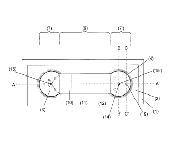
Fig. 1, Fig. 2a, Fig. 2b, and Fig. 2c show, in each case, a detail of a
heatable pane 1
according to the invention in the region of the electrical connection element
3. The
CA 02835553 2013-11-08
16
pane 1 is a 3-mm-thick thermally prestressed single-pane safety glass made of
soda
lime glass. The pane 1 has a width of 150 cm and a height of 80 cm. An
electrically
conductive structure 2 in the form of a heating conductor structure 2 is
printed on the
pane 1. The electrically conductive structure 2 contains silver particles and
glass frits. In
the edge region of the pane 1, the electrically conductive structure 2 is
widened to a
width of 10 mm and forms a contact surface for the electrical connection
element 3. In
the edge region of the pane 1, there is also a covering serigraph (not shown).
The
connection element 3 consists of two foot regions 7 and 7' that are connected
to each
other via the bridge 9. On the surfaces of the foot regions 7 and 7' facing
the substrate,
two contact surfaces 8' and 8" are arranged. In the region of the contact
surfaces 8' and
8", the solder material 4 effects a durable electrical and mechanical
connection between
the connection element 3 and the electrically conductive structure 2. The
solder material
4 contains 57 wt.-% bismuth, 40 wt.-% tin, and 3 wt.-% silver. The solder
material 4 is
arranged through a predefined volume and shape completely between the
electrical
connection element 3 and the electrically conductive structure 2. The solder
material 4
has a thickness of 250 pm. The electrical connection element 3 is made from
steel of the
material number 1.4509 in accordance with EN 10 088-2 (ThyssenKrupp Nirostae
4509)
with a coefficient of thermal expansion of 10.0 x 10⁻⁶/ C. Each of the contact
surfaces 8'
and 8" has the shape of a circular segment with a radius of 3 mm and a central
angle a
of 276 . The bridge 9 consists of three flat segments 10, 11, and 12. The
surface of each
of the two segments 10 and 12 facing the substrate encloses an angle of 40
with the
surface of the substrate 1. The segment 11 is arranged parallel to the surface
of the
substrate 1. The electrical connection element 3 has a length of 24 mm. The
two foot
regions 7 and 7' have a width of 6 mm; the bridge 9 has a width of 4 mm.
On each of the surfaces 13 and 13' of the foot regions 7 and 7' facing away
from the
substrate, a contact bump 14 is arranged. The contact bumps 14 are shaped as
hemispheres and have a height of 2.5 x 10⁴ m and a width of 5 x 10⁴ m. The
centers of
the contact bumps 14 are arranged vertical to the surface of the substrate
above the
circle centers of the contact surfaces 8' and 8". The soldering points 15 and
15 are
arranged at the points on the convex surface of the contact bumps 14 that have
the
greatest vertical distance from the surface of the substrate.
CA 02835553 2013-11-08
17
Three spacers 19 are arranged on each of the contact surfaces 8' and 8". The
spacers 19 are shaped as hemispheres and have a height of 2.5 x 10⁴ m and a
width of
x 104 m.
5 Steel of the material number 1.4509 in accordance with EN 10 088-2 has
good cold
forming properties and good welding properties with all methods except gas
welding.
The steel is used for construction of sound suppressor systems and exhaust gas
detoxification systems and is particularly suited for that due to its scaling
resistance to
more than 950 C and corrosion resistance against the stresses occurring in
the exhaust
.. gas system.
Fig. la depicts schematically a simplified representation of the heat
distribution around
the soldering points 15 and 15' during the soldering process. The circular
lines there are
isotherms. The shape of the contact surfaces 8' and 8" of the connection
elements 3 of
Fig. 1 is adapted to the heat distribution. Thus, the solder material 4 in the
region of the
contact surfaces 8' and 8" is uniformly and completely fuzed.
Fig. 3 depicts, in continuation of the exemplary embodiment of Fig. 1 and 2c,
an
alternative embodiment of the connection element 3 according to the invention.
The
electrical connection element 3 is provided on the surface facing the solder
material 4
with a silver-containing coating 5. This prevents spreading of the solder
material out
beyond the coating 5 and limits the outflow width b. In another embodiment, an
adhesion-promoting layer made, for example, of nickel and / or copper, can be
located
between the connection element 3 and the silver-containing layer 5. The
outflow width b
of the solder material 4 is less than 1 mm. No critical mechanical stresses
are observed
in the pane 1 due to the arrangement of the solder material 4. The connection
of the
pane 1 to the electrical connection element 3 via the electrically conductive
structure 2 is
durably stable.
Fig. 4 depicts, in continuation of the exemplary embodiment of Fig. 1 and 2c,
another
alternative embodiment of the connection element 3 according to the invention.
The
electrical connection element 3 contains, on the surface facing the solder
material 4, a
recess with a depth of 250 pm that forms a solder depot for the solder
material 4. It is
possible to completely prevent outflow of the solder material 4 from the
intermediate
space. The thermal stresses in the pane 1 are noncritical and a durable
electrical and
CA 02835553 2013-11-08
18
mechanical connection is provided between the connection element 3 and the
pane 1 via
the electrically conductive structure 2.
Fig. 5 depicts, in continuation of the exemplary embodiment of Fig. 1 and 2c,
another
alternative embodiment of the connection element 3 according to the invention.
The foot
regions 7 and 7' of the electrical connection element 3 are bent upward on the
edge
regions. The height of the upward bend of the edge region of the glass pane 1
is a
maximum of 400 pm. This forms a space for the solder material 4. The
predefined solder
material 4 forms a concave meniscus between the electrical connection element
3 and
the electrically conductive structure 2. It is possible to completely prevent
outflow of
solder material 4 from the intermediate space. The outflow width b, at roughly
0, is less
than zero, largely because of the meniscus formed. The thermal stresses in the
pane 1
are noncritical, and a durable electrical and mechanical connection is
provided between
the connection element 3 and the pane 1 via the electrically conductive
structure 2.
Fig. 6 depicts another alternative embodiment of the connection element 3
according to
the invention with contact surfaces 8' and 8" in the shape of circular
segments and
bridge 9 shaped flat in sections. The connection element 3 contains an iron-
containing
alloy with a coefficient of thermal expansion of 8 x 10-61 C. The material
thickness is
2 mm. In the region of the contact surfaces 8' and 8" of the connection
element 3, hat-
shaped compensation members 6 are applied with chromium-containing steel of
the
material number 1.4509 in accordance with EN 10 088-2 (ThyssenKrupp Nirosta
4509).
The maximum layer thickness of the hat-shaped compensation members 6 is 4 mm.
By
means of the compensation members, it is possible to adapt the coefficients of
thermal
expansion of the connection element 3 to the requirements of the pane 1 and of
the
solder material 4. The hat-shaped compensation members 6 result in improved
heat flow
during the production of the solder connection 4. The heating occurs primarily
in the
center of the contact surfaces 8' and 8". It is possible to further reduce the
outflow width
b of the solder material 4. Because of the low outflow width b of < 1 mm and
the adapted
coefficient of expansion, it is possible to further reduce the thermal
stresses in the pane
1. The thermal stresses in the pane 1 are noncritical, and a durable
electrical and
mechanical connection is provided between the connection element 3 and the
pane 1 via
the electrically conductive structure 2.
CA 02835553 2013-11-08
19
Fig. 7 depicts, in continuation of the exemplary embodiment of Fig. 1 and 2a,
an
alternative embodiment of the connection element 3 according to the invention.
The
bridge 9 is curved and has the profile of a circular arc with a radius of
curvature of
12 mm. The thermal stresses in the pane 1 are noncritical and a durable
electrical and
mechanical connection is provided between the connection element 3 and the
pane 1 via
the electrically conductive structure 2.
Fig. 8 depicts, in continuation of the exemplary embodiment of Fig. 1 and 2a,
another
alternative embodiment of the connection element 3 according to the invention.
The
bridge 9 is curved and changes its direction of curvature twice. Adjacent the
foot regions
7 and 7', the direction of curvature turns away from the substrate 1. Thus,
there are no
edges on the connections 16 and 16' between the contact surfaces 8' and 8" and
the
bottom of the bridge 9. The bottom of the connection element 3 has a
continuous
progression. The thermal stresses in the pane 1 are noncritical and a durable
electrical
and mechanical connection is provided between the connection element 3 and the
pane 1 via the electrically conductive structure 2.
Fig. 8a depicts, in continuation of the exemplary embodiment of Fig. 1 and 2a,
another
alternative embodiment of the connection element 3 according to the invention.
The
bridge 9 consists of two flat segments 22 and 23. The surface of each of the
two
segments 22 and 23 facing the substrate encloses an angle of 20 with the
surface of the
substrate 1. Together, the surfaces of the two segments 22 and 23 facing the
substrate
enclose an angle of 140 . The thermal stresses in the pane 1 are noncritical
and a
durable electrical and mechanical connection is provided between the
connection
element 3 and the pane 1 via the electrically conductive structure 2.
Fig. 9 and Fig. 9a depict, in each case, a detail of another embodiment of the
pane 1
according to the invention in the region of the electrical connection element
3. The
connection element 3 contains steel of the material number 1.4509 in
accordance with
EN 10 088-2 (ThyssenKrupp Nirosta 4509). The foot regions 7 and 7' are
connected to
each other via the bridge 9. The bridge 9 consists of three flatly shaped
segments 10,
11, and 12. Each of the contact surfaces 8' and 8" is shaped as a rectangle
with
semicircles arranged on opposite sides. The connection element 3 has a length
of
24 mm. The bridge 9 has a width of 4 mm. The contact surfaces 8' and 8" are 4
mm long
and 8 mm wide.
CA 02835553 2013-11-08
. 20
A contact bump 14 is arranged on each of the surfaces 13 and 13' of the foot
regions 7
and 7' turned away from the substrate 1. Each contact bump 14 is shaped as a
rectangular solid with a length of 3 mm and a width of 1 mm, with the surfaces
turned
away from the substrate 1 curved convexly. The height of the contact bumps is
0.6 mm.
The soldering points 15 and 15' are arranged at the points on the convex
surface of the
contact bumps 14 that have the greatest vertical distance from the surface of
the
substrate. Two spacers 19 that are shaped as hemispheres with a radius of 2.5
x 104 m
are arranged on each of the contact surfaces 8' and 8". No critical mechanical
stresses
were observed in the pane 1 due to the arrangement of the solder material 4.
The
connection of the pane 1 to the electrical connection element 3 via the
electrically
conductive structure 2 is durably stable.
Fig. 10 depicts a plan view of an alternative embodiment of the connection
element 3
according to the invention. The foot regions 7 and 7' are connected to each
other via the
bridge 9. The contact surfaces 8 and 8' are formed as circular segments with a
radius of
2.5 mm and a central angle a of 280 . The bridge 9 is curved. The width of the
bridge
becomes smaller starting from the connections 16 and 16' to the contact
surfaces 8 and
8' in the direction of the center of the bridge. The minimum width of the
bridge is 3 mm.
No critical mechanical stresses were observed in the pane 1 due to the
arrangement of
the solder material 4. The connection of the pane 1 to the electrical
connection element 3
via the electrically conductive structure 2 is durably stable.
In an alternative embodiment of the invention, the connection element 3 with
the contour
of Fig. 10 is not configured in the form of a bridge. Here, the connection
element 3 is
connected to the electrically conductive structure over its entire surface via
a contact
surface 8.
Fig. 11 and Fig. 11a depict, in each case, a detail of another alternative
embodiment of
the connection element 3 according to the invention. The two foot regions 7
and 7' are
connected to each other via the bridge 9. Each contact surface 8' and 8" is
shaped as a
circular segment with a radius of 2.5 mm and a central angle a von 286 . The
bridge 9
consists of two subelements. The subelements have, in each case, a curved
subregion
17 and 17' and a flat subregion 18 and 18'. The bridge 9 is connected to the
foot region 7
via the subregion 17 and to the foot region 7' via the subregion 17'. The
directions of
CA 02835553 2013-11-08
= 21
curvature of the subregions 17 and 17' turn away from the substrate 1. The
flat
subregions 18 and 18' are arranged perpendicular to the surface of the
substrate and are
in direct contact with each other. The contact bumps 14 are shaped as
hemispheres with
a radius of 5 x 10⁻⁴ m. The spacers 19 are shaped as hemispheres with a radius
of 2.5 x
10-4 m. The connection element 3 has a length of 10 mm. The foot regions 7 and
7' have
a width of 5 mm; the bridge 9 has a width of 3 mm. The height of the bridge 9
from the
surface of the substrate 1 is 3 mm. The height of the bridge 9 can preferably
be between
1 mm and 5 mm. No critical mechanical stresses were observed in the pane 1 due
to the
arrangement of the solder material 4. The connection of the pane 1 to the
electrical
connection element 3 via the electrically conductive structure 2 is durably
stable.
Fig. 12 depicts a plan view of another alternative embodiment of the
connection element
3 according to the invention. The two foot regions 7 and 7' are connected to
each other
via a curved bridge 9. Each contact surface 8' and 8" is shaped as a circle
with a radius
of 2.5 mm. The two connections 16 and 16' between the foot regions 7 and 7'
and the
bridge 9 are arranged completely on different sides of the direct connecting
line between
the circle centers of the contact surfaces 8' and 8". The projection of the
bridge into the
plane of the substrate surface is curved. In this case, the direction of
curvature changes
in the center of the bridge. Laterally, in the center of the bridge 9, are
arranged two
convexities opposite each other in the shape of circular segments with radii
of 2 mm. The
radii of the convexities can preferably be between 1 mm and 3 mm. The
convexities can,
for example, also have a rectangular shape with a preferred length and width
from 1 mm
to 6 mm. On the region of the bridge 9 that is delimited by the edges of the
convexities,
an electrically conductive material for connection to the onboard electrical
system can,
for example, be applied, by welding or crimping, for example. No critical
mechanical
stresses are observed in the pane 1 due to the arrangement of the solder
material 4. The
connection of the pane 1 to the electrical connection element 3 via the
electrically
conductive structure 2 is durably stable.
Fig. 13 and Fig. 13a depict, in each case, a detail of another alternative
embodiment of
the connection element 3 according to the invention. The connection element 3
is
connected over its entire surface to the electrically conductive structure 2
via a contact
surface 8. The contact surface 8 is shaped as a rectangle with semicircles
arranged on
opposite sides. The contact surface has a length of 14 mm and a width of 5 mm.
The
connection element 3 is bent upward all around in the edge region 20. The
height of the
CA 02835553 2013-11-08
. 22
edge region 20 from the glass pane 1 is 2.5 mm. The height of the edge region
20 can,
in alternative embodiments of the invention, preferably be between 1 mm and 3
mm. An
extension element 21 is arranged on the bent-up edge on one of the two
straight sides of
the connection element 3. The extension element 21 consists of a curved
subregion and
a flat subregion. The extension element 21 is connected to the edge region 20
of the
connection element 3 via the curved subregion and the direction of curvature
is toward
the opposite side of the connection element 3. The extension element 21 has,
in the plan
view, a length of 11 mm and a width of 6 mm. The extension element 21 can
preferably
have a length between 5 mm and 20 mm, particularly preferably between 7 mm and
15 mm, and a width of 2 mm to 10 mm, particularly preferably from 4 mm to 8
mm. An
electrically conductive material for connection to the onboard electrical
system can, for
example, be applied on the extension element 21, for example, by wielding,
crimping, or
in the form of a plug connector. No critical mechanical stresses are observed
in the pane
1 due to the arrangement of the solder material 4. The connection of the pane
1 to the
electrical connection element 3 via the electrically conductive structure 2 is
durably
stable.
Fig. 14 depicts in detail a method according to the invention for production
of a pane 1
with an electrical connection element 3. An example of the method according to
the
invention for production of a pane with an electrical connection element 3 is
presented
there. As the first step, it is necessary to portion the solder material 4
according to shape
and volume. The portioned solder material 4 is arranged on the contact surface
8 or the
contact surfaces 8' and 8" of the electrical connection element 3. The
electrical
connection element 3 is arranged with the solder material 4 on the
electrically conductive
structure 2. A durable connection of the electrical connection element 3 to
the electrically
conductive structure 2 and, thus, to the pane 1 takes place through the input
of energy
on the soldering points 15 and 15'.
CA 02835553 2013-11-08
. 23
Example
Test specimens were produced with the pane 1 (thickness 3 mm, width 150 cm,
and
height 80 cm), the electrically conductive structure 2 in the form of a
heating conductor
structure, the electrical connection element 3 according to Fig. 1, the silver
layer 5 on the
contact surfaces 8' and 8" of the connection element 3, and the solder
material 4. The
material thickness of the connection element 3 was 0.8 mm. The connection
element 3
contained steel of the material number 1.4509 in accordance with EN 10 088-2
(ThyssenKrupp Nirosta 4509). Three spacers 19 were arranged on each of the
contact
surfaces 8' and 8". Each soldering point 15 and 15' was arranged on a contact
bump 14.
The solder material 4 was applied in advance as a platelet with fixed layer
thickness,
volume, and shape on the contact surfaces 8' and 8"of the connection element
3. The
connection element 3 was applied with the solder material 4 applied on the
electrically
conductive structure 2. The connection element 3 was soldered onto the
electrically
conductive structure 2 at a temperature of 200 C and a processing time of 2
seconds.
Outflow of the solder material 4 from the intermediate space between the
electrical
connection element 3 and the electrically conductive structure 2, which
exceeded a layer
thickness t of 50 pm, was observed only to a maximum outflow width of b = 0.4
mm. The
dimensions and compositions of the electrical connection element 3, the silver
layer 5 on
the contact surfaces 8' and 8" of the connection element 3, and the solder
material 4 are
found in Table 1. No critical mechanical stresses were observed in the pane 1
due to the
arrangement of the solder material 4, predefined by the connection element 3
and the
electrically conductive structure 2. The connection of the pane 1 to the
electrical
connection element 3 via the electrically conductive structure 2 was durably
stable.
With all specimens, it was possible to observe, with a temperature difference
from
+80 C to -30 C, that no glass substrate 1 broke or showed damage. It was
possible to
demonstrate that, shortly after soldering, these panes 1 with the soldered
connection
element 3 were stable against a sudden temperature drop.
In addition, test specimens were executed with a second composition of the
electrical
connection element 3. Here, the connection element 3 contained an iron-nickel-
cobalt
alloy. The dimensions and compositions of the electrical connection element 3,
the silver
layer 5 on the contact surfaces 8' and 8" of the connection element 3, and the
solder
material 4 are found in Table 2. With the outflow of the solder material 4
from the
CA 02835553 2013-11-08
24
intermediate space between the electrical connection element 3 and the
electrically
conductive structure 2, which exceeded a layer thickness t of 50 pm, an
average outflow
width b = 0.4 mm was obtained. Here as well, it was possible to observe that,
with a
temperature difference from +80 C to -30 C, no glass substrate 1 broke or
showed
damage. It was possible to demonstrate that, shortly after soldering, these
panes 1 with
the soldered connection element 3 were stable against a sudden temperature
drop.
In addition, test specimens were executed with a third composition of the
electrical
connection element 3. Here, the connection element 3 contained an iron-nickel
alloy.
The dimensions and compositions of the electrical connection element 3, the
silver layer
5 on the contact surfaces 8' and 8" of the connection element 3, and the
solder material
4 are found in Table 3. With the outflow of the solder material 4 from the
intermediate
space between the electrical connection element 3 and the electrically
conductive
structure 2, which exceeded a layer thickness t of 50 pm, an average outflow
width
b = 0.4 mm was obtained. Here as well, it was possible to observe that, with a
temperature difference from +80 C to -30 C, no glass substrate 1 broke or
showed
damage. It was possible to demonstrate that, shortly after soldering, these
panes 1 with
the soldered connection element 3 were stable against a sudden temperature
drop.
Table 1
Components Material Example
Connection element 3
Steel of material no. 1.4509 in accordance with
EN 10 088-2 with the composition:
Iron (wt.-%) 78.87
Carbon (wt.-%) 0.03
Chromium (wt.-%) 18.5
Titanium (wt.-%) 0.6
Niobium (wt.-%) 1
Manganese (wt.-%) 1
CTE (coefficient of thermal expansion) 10
(10-6/00 for 0 C ¨100 C)
Difference between CTE of the connection 1.7
element and substrate (10-6/ C for 0 C - 100 C)
Thickness of the connection element (m) 8.0 x 10⁴
Wetting layer 5
Silver (wt.-c/o) 100
Thickness of the layer (m) 7.0 x 10⁻⁶
CA 02835553 2013-11-08
Components Material Example
Solder material 4
Tin (wt.-%) 40
Bismuth (wt.-%) 57
Silver (wt.-%) 3
Thickness of the solder layer in (m) 250 x 10-6 ,
The thickness of the wetting layer and the solder 257 x 10-6
layer (m)
Glass substrate 1
(Soda lime glass)
CTE (10-61 C for 0 C ¨ 320 C) 8.3
Table 2
Components Material Example
Connection element 3
Iron (wt.-%) 54
Nickel (wt.-%) 29
Cobalt (wt.-%) 17
CTE (coefficient of thermal expansion) 5.1
(10-6/ C for 0 C ¨ 100 C)
Difference between CIE of the connection 3.2
element and substrate (10-6/ C for 0 C - 100 C)
Thickness of the connection element (m) 8.0 x 10⁻⁴
Wetting layer 5
Silver (wt.-%) 100
Thickness of the layer (m) 7.0 x 10⁻⁶
Solder material 4
Tin (wt.-%) 40
Bismuth (wt.-%) 57
Silver (wt.-%) 3
Thickness of the solder layer in (m) 250 x 10-6
The thickness of the wetting layer and the solder 257 x 10-6
layer (m)
Glass substrate 1
(Soda lime glass)
CTE (10-6/ C for 0 C ¨ 320 C) 8.3
CA 02835553 2013-11-08
26
Table 3
Components Material Example
Connection element 3
Iron (wt.-%) 65
Nickel (wt.-%) 35
CTE (coefficient of thermal expansion) 1.7
(10-6/ C for 0 C ¨100 C)
Difference between CTE of the connection 6.6
element and substrate (10-6/ C for 0 C - 100 C)
Thickness of the connection element (m) 8.0 x 10⁴
Wetting layer 5
Silver (wt.-%) 100
Thickness of the layer (m) 7.0 x 10⁻⁶
Solder material 4
Tin (wt.-%) 40
Bismuth (wt.-%) 57
Silver (wt.-%) 3
Thickness of the solder layer in (m) 250 x 10-6
The thickness of the wetting layer and the solder 257 x 10-6
layer (m)
Glass substrate 1
(Soda lime glass)
CTE (10-6/ C for 0 C¨ 320 C) 8.3
Comparative Example
The comparative example was carried out the same as the example. The
difference
resided in the shape of the connection element. This was, according to the
prior art,
connected to the electrically conductive structure via a rectangular contact
surface. The
shape of the contact surface was not adapted to the profile of the heat
distribution. No
spacers were arranged on the contact surface. The soldering points 15 and 15'
were not
arranged on contact bumps. The dimensions and components of the electrical
connection element 3, of the metal layer on the contact surface of the
connection
element 3, and of the solder material 4 are found in Table 4. The connection
element 3
was soldered to the electrically conductive structure 2 in accordance with
conventional
methods by means of the solder material 4. With the outflow of the solder
material 4 from
the intermediate space between the electrical connection element 3 and the
electrically
conductive structure 2, which exceeded a layer thickness t of 50 pm, an
average outflow
width b = 2 mm to 3 mm was obtained.
CA 02835553 2013-11-08
27
With a sudden temperature difference from +80 C to -30 C, it was observed
that the
glass substrates 1 had major damage shortly after soldering.
Table 4
Components Material Comparative
example
Connection element 3 Steel of material no. 1.4509 in accordance with
EN 10 088-2 with the composition:
Iron (wt.-%) 78.87
Carbon (wt.-%) 0.03
Chromium (wt.-%) 18.5
Titanium (wt.-%) 0.6
Niobium (wt.-%) 1
Manganese (wt.-%) 1
CTE (coefficient of thermal expansion) 10
(10-6/ C for 0 C ¨ 100 C)
Difference between CTE of the connection 1.7
element and the substrate
(10-6PC for 0 C - 100 C)
Thickness of the connection element (m) 8.0 x 10⁻⁴
Wetting layer 5
Silver (wt.-%) 100
Thickness of the layer (m) 7.0 x 10⁻⁶
Solder material 4
Tin (wt.-%) 40
Bismuth (wt.-%) 57
Silver (wt.-%) 3
Thickness of the solder layer in (m) 250 x 10-6
The thickness of the wetting layer and the 257 x 10-6
solder layer (m)
Glass substrate 1
(Soda lime glass)
CTE (10-6PC for 0 C¨ 320 C) 8.3
It was demonstrated that panes according to the invention with glass
substrates 1 and
electrical connection elements 3 according to the invention had better
stability against
sudden temperature differences.
This result was unexpected and surprising for the person skilled in the art.
CA 02835553 2013-11-08
28
List of Reference Characters
(1) Pane
(2) Electrically conductive structure
(3) Electrical connection element
(4) Solder material
(5) Wetting layer
(6) Compensation member
(7) Foot region of the electrical connection element 3
(7') Foot region of the electrical connection element 3
(8) Contact surface of the connection element 3
(8') Contact surface of the connection element 3
(8") Contact surface of the connection element 3
(9) Bridge between the foot regions 7 and 7'
(10) Segment of the bridge 9
(11) Segment of the bridge 9
(12) Segment of the bridge 9
(13) Surface of the foot region 7 turned away from the substrate 1
(13') Surface of the foot region 7' turned away from the substrate 1
(14) Contact bump
(15) Soldering point
(15') Soldering point
(16) Connection of contact surface 8 and the bottom of the bridge 9
(16') Connection the contact surface 8' and the bottom of the bridge 9
(17) Subregion of the bridge 9
(17') Subregion of the bridge 9
(18) Subregion of the bridge 9
(18') Subregion of the bridge 9
(19) Spacer
(20) Edge region of the connection element 3
(21) Extension element
(22) Segment of the bridge 9
(23) Segment of the bridge 9
CA 02835553 2013-11-08
. 29
a Central angle of a circular segment of a contact surface 8'
b Maximum outflow width of the solder material
t Limiting thickness of the solder material
A-A' Section line
B-B' Section line
C-C' Section line
D-D' Section line
E-E' Section line
F-F' Section line