Note: Descriptions are shown in the official language in which they were submitted.
CA 02836335 2013-12-09
APPARATUS AND METHOD FOR CONTROLLING CIRCULATING
CURRENT IN AN INVERTER SYSTEM
BACKGROUND
Power converters are used in aircraft electrical power systems as well as in
power
systems for other apparatus. The electrical power systems on current
commercial aircraft
are primarily provided by 400 Hz, three-phase 115V or 230V AC power sources.
The
power system may include one or more alternative low voltage DC power sources,
such
as a fuel cell stack or a battery, which provides input power to a pulse width
modulated
(PWM) power conversion system. Multiphase voltage outputs, such as three-phase
voltages, maybe provided to an aircraft electric power distribution system,
which
provides the electrical power to a downstream distribution system. The
downstream
distribution system may have loads of various types, including, but not
limited to, three-
phase, single-phase, or another conversion system with DC loads, etc.
Many power converters, however, are not fully optimized for aircraft
applications.
Such power converters may be large and heavy, increasing the weight of the
aircraft and
limiting the volume available to other aircraft components. To address this
issue, power
converters may include paralleled or interleaved inverters. By using
paralleled or
interleaved inverters, the conversion systems may achieve higher power while
concurrently using lower rating devices, thus also achieving higher
efficiency, higher
power density (measured in kW/kg), and weight and volume savings.
Additionally,
interleaved converters improve the harmonic reduction compared with non-
interleaved
converters. However, such converter systems may generate circulating current,
which
may degrade the performance or cause malfunctions, even to the point of
damaging the
user equipment connected to the power bus.
In power converters employing paralleled or interleaved inverters, the
inverter
outputs may be connected to inductive components to limit the circulating
current.
However, the inductive components often do not work well in low frequency
circulating
current. The low frequency circulating currents may cause saturation of the
cores of the
1
CA 02836335 2015-10-07
inductive components. Saturation of the cores may reduce the performance of
the power
converter as well as disable the conversion system.
Also in designing the power converter, large magnetizing inductances may be
desired
to reduce core loss and better limit high frequency circulating currents.
However, this may
require advanced and accurate knowledge of system parameters, which makes the
design
process complicated and time-consuming. For example, the complexity of control
system
design may be caused by a reduced margin on the flux of a given magnetic core
when a large
magnetizing inductance is desired.
Therefore, there are at least two problems associated with power conversion
systems.
They may experience reduced performance when used with high transient loads.
Also, the
design process may complicated and time-consuming.
SUMMARY
A power conversion system is disclosed, in certain illustrative embodiments,
that
provides multiphase power, including phase voltages for each phase of the
multiphase power.
The system may include a plurality of inverters that generate PWM output
voltages based on
PWM control signals, and a plurality of inductive components that are
configured to receive
the PWM output voltages to generate the phase voltages. The PWM output
voltages may
cause circulating current flows through the inductive components. A voltage
controller may
be employed that is responsive to the phase voltages to generate voltage
modulation signals
corresponding to the phase voltages. A plurality of current sharing channels
may be
respectively associated with each of the plurality of inductive components and
may be
configured generate current sharing modulation signals in response to the
circulating current
flows. The PWM control signals may be generated based on modulation signals
obtained by
combining the current sharing modulation signals and voltage modulation
signals.
The disclosure also describes embodiments of a power conversion system
configured
to supply multiphase power having a phase voltage respectively associated with
each phase of
2
CA 02836335 2015-10-07
the multiphase power. The power conversion system includes a plurality of
inverters
configured to generate PWM output voltages for each phase voltage in response
to PWM
control signals, and a plurality of inductive components configured to receive
the PWM
output voltages to generate the phase voltages, wherein the PWM output
voltages result in a
plurality of circulating current flows in the plurality of inductive
components. The power
conversion system also includes a voltage controller responsive to generate
voltage
modulation signals for each phase voltage, and a plurality of current sharing
channels
respectively associated with each of the plurality of inductive components,
wherein the
plurality of current sharing channels are configured to generate current
sharing modulation
signals in response to the plurality of circulating current flows. The power
conversion system
also includes a carrier reference circuit configured to generate the PWM
control signals in
response to modulation signals, wherein the modulation signals are obtained by
combining the
current sharing modulation signals and voltage modulation signals.
The inductive components may include a plurality of inter-cell transformers.
The inductive components may include a plurality of inductors.
The plurality of inverters may include first and second inverters, wherein the
first
and second inverters generate interleaved three-phase PWM output voltages.
The plurality of inter-cell transformers may be configured to provide three-
phase
supply voltages using interleaved three-phase PWM output voltages from first
and
second inverters.
Each of the first and second inverters further may provide a neutral phase
voltage.
The power conversion system may further include a current sensing circuit
having
a plurality of current sensors configured to provide circulating current
signals to
the current sharing channels for each of the plurality of inductive
components.
3
CA 02836335 2015-10-07
The current sharing channels may include a resonant fundamental frequency
controller having a center frequency proximate a fundamental frequency of the
phase voltages.
The current sharing channels may have a frequency transform response generally
corresponding to:
((
KI s
C(s)= k+¨ + + , , +Cph* Kf0+ K f s
s + Awls+ Oij s2 ACO S+ co 2
DC Low frequency Fundamental frequency
where
k(s + col)
Cph=
(s + w2)2
wherein co/ defines a center frequency of a low-frequency filter, cof defines
a center
frequency of a fundamental frequency filter, Ao)/ defines a bandwidth of the
low-
frequency filter, Acof defines a bandwidth of the fundamental frequency
filter, K10
and K10 define magnitudes of pass bands of the low-frequency filter and
fundamental frequency filter, respectively, K1 and K1 define peak gains of the
low-
frequency filter and fundamental frequency filter, respectively, and C ph(s)
is a
phase delay compensator providing phase compensation around the fundamental
frequency.
The power conversion system may further include a DC power source configured
to provide input power to the plurality of inverters, wherein the plurality of
inverters share a common DC bus.
The disclosure also describes embodiments of a control system for a power
conversion
system. The control system includes a voltage controller responsive to three-
phase voltage
4
CA 02836335 2015-10-07
signals to generate corresponding voltage modulation signals, current sharing
channels
responsive to a plurality of circulating currents from a plurality of
inductive components,
wherein the inductive components are associated with respective phases of the
three-phase
voltage signals, wherein the current sharing channels generate current sharing
modulation
signals respectively associated with each phase of the three-phase voltage
signals using the
plurality of circulating currents from the plurality of inductive components.
The control
system also includes a plurality of combiner circuits, wherein each combiner
circuit is
associated with a phase of the three-phase voltage signals, and wherein the
combiner circuits
combine the voltage modulation signals and the current sharing modulation
signals
respectively associated with each phase of the three-phase voltage signals to
generate PWM
control signals.
The current sharing channels may be configured to receive circulating currents
from a plurality of inter-cell transformers.
The current sharing channels may be configured to receive circulating currents
from a plurality of inductors.
The current sharing channels may include a resonant frequency controller
having a
center frequency proximate a fundamental frequency of each phase of the three-
phase voltage signals.
Each current sharing channel may have a frequency transform response generally
corresponding to:
(1(1\ ( s
C(S)= 2 2 Klo+ C ph * K f 0+
l< s
A
S S LAW+
S2 + ACOf S+ co f2
DC Low frequency Fundamental
frequency
where
5
CA 02836335 2015-10-07
k(s + col)
Ch =
(s + W2)2
wherein col defines a center frequency of a low-frequency filter, cof defines
a center
frequency of a fundamental frequency filter, Act)/ defines a bandwidth of the
low-
frequency filter, Acof defines a bandwidth of the fundamental frequency
filter, 1(10
and K10 define magnitudes of pass bands of the low-frequency filter and
fundamental frequency filter, respectively, K, and Kf define peak gains of the
low-
frequency filter and fundamental frequency filter, respectively, and Ph
s a
phase delay compensator providing phase compensation around the fundamental
frequency.
The disclosure also describes embodiments of a power conversion system
configured
to supply multiphase power, the multiphase power having a phase voltage
respectively
associated with each phase of the multiphase power. The power conversion
system includes a
PWM drive circuit, a plurality of inverters having inputs coupled to the PWM
drive circuit, a
plurality of inductive components coupled to PWM voltage outputs of the
plurality of
inverters, a plurality of power supply output terminals coupled to the outputs
of the plurality
of the inductive components, a plurality of current sensors coupled to the
plurality of
inductive components, a voltage controller coupled to the plurality of
inductive components, a
current sharing system coupled to the plurality of current sensors, a combiner
circuit coupled
to outputs of the voltage controller and to outputs of the current sharing
system, and a drive
circuit coupled to the combiner circuit.
The plurality of inductive components may include inter-cell transformers.
The plurality of inductive components may include inductors.
6
CA 02836335 2015-10-07
The plurality of current sensors may be coupled to the inter-cell transformers
to
provide signals corresponding to twice a circulating current flowing through
each
of the inter-cell transformers.
The current sharing system may include a plurality of current sharing
controllers
arranged in pairs, wherein each pair of the plurality of current sharing
controllers
is coupled to a respective current sensor.
Each current sharing controller of each pair of current sharing controllers
may
include a resonant controller having a center frequency proximate a
fundamental
frequency of voltages at the plurality of power supply terminals.
The power conversion system may further include a DC power source coupled to
the plurality of inverters, wherein the plurality of inverters are coupled to
a
common DC bus.
The disclosure also describes embodiments of a method for controlling a
multiphase
power conversion system. The method may involve generating voltage modulation
signals in
response to each phase voltage of the multiphase power, detecting circulating
currents flowing
through a plurality of inter-cell transformers, each of which are associated
with a respective
phase voltage, applying a controller to the detected circulating currents
pursuant to generating
current sharing modulation signals corresponding to the circulating currents,
and combining
voltage modulation signals and current sharing modulation signals to generate
PWM control
signals.
Applying the controller may involve applying a resonant controller at a center
frequency proximate a fundamental frequency of each phase of the multiphase
power.
7
CA 02836335 2015-10-07
Applying the controller may involve applying a controller having a transform
frequency response generally corresponding to:
((
Ki s
C(s)= k p ¨ + Kip+ , + C ph* K f 0+ K S
S ANIS+ C01- 2 A
S LAWS+ CO'
2j
DC Low frequency
Fundamental frequency
where
k(s + col)
Cph =
(s CO2)2
wherein on defines a center frequency of a low-frequency filter, oy defines a
center
frequency of a fundamental frequency filter, don defines a bandwidth of the
low-
frequency filter, zkof defines a bandwidth of the fundamental frequency
filter, Kro
and K10 define magnitudes of pass bands of the low-frequency filter and
fundamental frequency filter, respectively, K1 and Ki define peak gains of the
low-
frequency filter and fundamental frequency filter, respectively, and Ph(s) is
a
phase delay compensator providing phase compensation around the fundamental
frequency.
These and other features and functions may be achieved independently in
various
embodiments of the present disclosure or may be combined to form yet other
embodiments as
can be understood by reference to the following description and drawings.
8
CA 02836335 2015-10-07
BRIEF DESCRIPTION OF THE DRAWINGS
Figure 1 is a block diagram of a power conversion system that uses inter-cell
transformers as inductive components.
Figure 2 illustrates one manner in which the inter-cell transformers of Figure
1 may be
coupled within the power conversion system.
Figure 3 illustrates a voltage control system that may be employed within the
power
conversion system of Figure 1.
Figure 4 illustrates one manner of executing sequence decomposition.
Figure 5 illustrates an algorithm configured to execute the sequence
decomposition
shown in Figure 4.
Figure 6 illustrates current sharing channels that may be employed in the
power
conversion system of Figure 1.
Figures 7a - 7c are Bode plots for one example of a current sharing
controller.
Figure 8 illustrates a power conversion system in which various signal
processing
operations take place in a digital signal processor (DSP).
Figure 9 shows a method for controlling a power conversion system.
Figures 10a - 10b are exemplary signal graphs associated with voltages of a
power
conversion system that does not implement a control system of the type shown
and described
in connection with one or more of Figures 1 - 9.
Figure 10c are signal graphs representing flux variation in the cores of inter-
cell
transformers in the power system that does not implement the control system of
the type
shown and described in connection with one or more of Figures 1 - 9.
9
CA 02836335 2013-12-09
Figures ha - lib are exemplary signal graphs associated with voltages of a
power
conversion system having a control system of the type shown and described in
connection
with one or more of Figures 1 - 9.
Figure 11c are signal graphs representing flux variations in the cores of
inter-cell
transformers in a power system that does implement the control system of the
type shown
and described in connection with one or more of Figures 1 - 9.
Figure 12 is a flow chart illustrating how the power conversion system may be
incorporated in the context of the design and operation of an aircraft.
Figure 13 is a block diagram illustrating an aircraft that incorporates the
power
conversion system.
DESCRIPTION
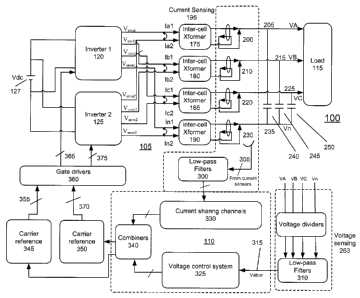
Figure 1 is a block diagram of a power conversion system 100. The power
conversion system 100 includes a power drive section 105 and a control system
110. The
power conversion system 100 provides multiphase power to load 115. Although
the
following embodiments are described in the context of a three-phase inverter
system that
supplies three voltages phased approximately 1200 from one another, the
embodiments
may be extended to inverter systems having more or less than three-phases.
EXAMPLE POWER DRIVE SECTION
The power drive section 105 includes a plurality of inverters, each having a
plurality of PWM output voltages. The number of PWM output voltages provided
by
each inverter is at least as large as the number of phases used to drive the
load 115.
In the exemplary power conversion system 100 of Figure 1, the power drive
section 105 includes a first inverter 120 and a second inverter 125, which
receive DC
power from a DC source 127. The first inverter 120 and second inverter 125
share a
common DC bus of the DC source 127.
The first inverter 120 provides a first PWM output voltage Vulva', a second
PWM
output voltage V1nvb1, and a third PWM output voltage Vulva. Similarly, the
second
CA 02836335 2013-12-09
inverter 125 provides a first PWM output Vinva, a second PWM output voltage
Vinvb2, and
a third PWM output voltage Vinvc2. The PWM output voltages are interleaved.
The power conversion system 100 of the example is configured as a four-leg
system. As such, the first inverter 120 and second inverter 125 each include
neutral
PWM output voltages. More particularly, first inverter 120 provides a first
neutral PWM
output voltage VInvnl, and second inverter 125 provides a second neutral PWM
output
voltage Vinvn2- Such three-phase, 4-leg inverters may be used to maintain a
desired
sinusoidal output voltage waveform on each phase output over a desired range
of loading
conditions and transients. The power conversion system 100 need not be
configured as
such a four-leg system but will be discussed in the context of such an
architecture.
The power drive section 105 also includes a plurality of inductive components.
The inductive components may be in the form of inductors or inter-cell
transformers. For
purposes of describing the exemplary power conversion system 100, inter-cell
transformers are used as the inductive components. However, the inter-cell
transformers
of Figure 1 may be replaced by inductors depending on system design
parameters.
In Figure 1, a first inter-cell transformer 175 is coupled to receive the
first PWM
output voltage Vinval from first inverter 120 and the first PWM output voltage
Vi1va2 from
second inverter 125. A second inter-cell transformer 180 is coupled to receive
the second
PWM output voltage Vino' and the second PWM output voltage Vinvb2. A third
inter-cell
transformer 185 is coupled to receive the third PWM output voltage Vinvci and
third PWM
output voltage Vinvc2. A fourth inter-cell transformer 190 is coupled to
receive neutral
PWM output voltage Vinvn1 and neutral PWM output voltage Vinvn2-
Figure 2 shows one manner in which the inter-cell transformers may be coupled
with a power drive section 105. As shown, the output terminals of first
inverter 120 and
second inverter 125 are connected to respective terminals of the first inter-
cell
transformer 175, second inter-cell transformer 180, third inter-cell
transformer 185, and
the fourth inter-cell transformer 190. The dots of the inter-cell transformers
show the
coupling configuration of the transformer windings. The inter-cell
transformers of this
example are configured as differential mode inductors. While the magnetizing
inductance
is used to limit the circulating current, the leakage inductance is used as
inductance for an
11
CA 02836335 2013-12-09
output LC filter respectively associated with each voltage phase. When the
inter-cell
transformers use a high permeability core, a high magnetizing inductance is
obtained.
Thus, a small circulating current and high efficiency may be achieved.
Returning to Figure 1, the parallel operation of inverters 120 and 125 results
in
circulating currents in each inter-cell transformer. In the example, the
circulating current
through first inter-cell transformer 175 is the current difference (Ial-1a2)
between the
terminal carrying the first PWM output voltage Vinval and the terminal
carrying the first
PWM output voltage Vinva2. The circulating current through second inter-cell
transformer
180 is the current difference (Ibl-1b2) between the terminal carrying the
second PWM
output voltage Vinvb1 and the terminal carrying the second PWM output voltage
Vllivb2.
The circulating current through third inter-cell transformer 185 is the
current difference
(Icl-1c2) between the terminal carrying the third PWM output voltage V11vc1
and the
terminal carrying the third PWM output voltage Vinvc2. The circulating current
through
the fourth inter-cell transformer 190 is the difference (Inl-1n2) between the
terminal
carrying neutral PWM output voltage Vinvnl and the terminal carrying neutral
PWM
output voltage Vinvn2.
The outputs of the inter-cell transformers are provided to a current sensing
circuit
195. Although the current sensing circuit 195 is shown at the outputs of the
inter-cell
transformers, it may alternatively be placed to monitor the current at the
inputs of the
inter-cell transformers.
The current sensing circuit 195 may include a plurality of current sensors,
each
respectively associated with a voltage phase. Here, each inter-cell
transformer includes
two output terminals. The two output terminal of each inter-cell transformer
are coupled
to a respective Hall effect current sensor before merging through the Hall
effect current
sensor in reverse directions at nodes coupled to provide the multiphase power
to the load.
In this way, the current difference, or the circulating current, between the
two output
currents from each inter-cell transformer is acquired.
In Figure 1 and Figure 2, a first current sensor 200 is coupled to the output
terminals of first inter-cell transformer 175, where a first phase supply
voltage VA is
provided to the load 115 at node 205. A second current sensor 210 is coupled
to the
12
CA 02836335 2013-12-09
output terminals of second inter-cell transformer 180, where a second phase
supply
voltage VB is provided to the load 115 at node 215. A third current sensor 220
is coupled
to the output terminals of third inter-cell transformer 185, where a third
phase supply
voltage VC is provided to the load 115 at node 225. A fourth current sensor
230 is
coupled to the output terminal of fourth inter-cell transformer 190, where a
neutral phase
voltage Vn is provided to the load 115 at node 235. As such, three-phase
supply voltages
(VA, VB, VC) are provided to the load 115.
The inter-cell transformers suppress high-frequency circulating current. Low
frequency circulating current passes through each inter-cell transformer and
is sensed by
the current sensing circuit 195 for low-frequency circulating current control.
A capacitor is coupled to each node carrying a voltage to the load 115. The
respective capacitor for each voltage supply phase and the inductance of the
corresponding inter-cell transformer may be used as a filter for the voltage
supply phase.
In Figure 2, a first capacitor 240 is coupled to node 205 and forms a filter
with the
leakage inductance of the first inter-cell transformer 175 and the fourth
inter-cell
transformer 190 to filter output phase voltage VA. A second capacitor 245 is
coupled to
node 215 and forms a filter with the leakage inductance of the second inter-
cell
transformer 180 and the fourth inter-cell transformer 190 to filter output
phase voltage
VB. A third capacitor 250 is coupled to node 225 and forms a filter with the
leakage
inductance of the third inter-cell transformer 185 and the fourth inter-cell
transformer 190
to filter output phase voltage VC.
The power drive section 105 may also include a voltage sensing circuit 263. As
shown in Figure 2, the voltage sensing circuit 263 includes a plurality of
voltage dividers
placed across capacitors 240, 245, and 250 to monitor the magnitudes of supply
voltages
VA, VB, and VC with respect to Vn. The divided voltage signals are provided to
power
control system 110. In this example, the voltage divider includes resistors
connected
across each capacitor.
The power drive section 105 may include low-pass filters respectively
associated
with the current sensing circuit 195 and the voltage sensing circuit 263. In
the example of
Figure 1, low-pass filters 300 are coupled to receive signals from the current
sensing
13
CA 02836335 2013-12-09
circuit 195 along current sensing bus 305. Low-pass filters 310 receive
voltages from the
voltage sensing circuit 263 and provide output voltages Van, Vbn, and Vcn
along voltage
sensing bus 315.
THE CONTROL SYSTEM
Referring again to Figure 1, the control system 110 is coupled to receive
voltage
signals Van, Vbn, Vcn on voltage sensing bus 315 for provision to a voltage
control
system 325. The control system 110 is also coupled to receive signals from the
current
sensing circuit 195 for provision to a plurality of current sharing channels
330. The
outputs of the current sharing channels 330 and the outputs of the voltage
control system
325 are provided to a plurality of combiners 340. The outputs of the combiners
340 are
modulation signals that are obtained by combining current sharing modulation
signals
generated by the current sharing channel 330 with voltage modulation signals
generated
by the voltage control system 325. These modulation signals are supplied for
comparison
to carrier reference signals at carrier reference 345 and carrier reference
350. Carrier
reference 345 generates PWM control signals 355 to gate drivers 360, which
provide gate
drive signals 365 to first inverter 120. In a similar manner, carrier
reference 350
generates PWM control signals 370 to gate drivers 360, which provide gate
drive signals
375 to second inverter 125.
Exemplary voltage control system
An exemplary voltage control system 325 is shown in Figure 3. In this example,
voltage signals Van, Vbn, Vcn are supplied to analog-to-digital converter 398,
which
converts the received voltage signals to digital signals va, vb, and vc on
digital signal bus
327. The digital signals on digital signal bus 327 are provided to a sequence
decomposer
400. The signals generated by the sequence decomposer 400 are provided to the
input of
an abc-to-dq transformer 405. The abc-to-dq transformer 405 transforms the
digital
signals at its inputs into digital signals that may be manipulated in a dq
coordinate system.
Such manipulations in this example are executed by a voltage controller 410,
which
receives the dq signals from the abc-to-dq transformer 405. The voltage
controller 410
14
CA 02836335 2013-12-09
executes operations on the dq signals from the abc-to-dq transformer 405 to
generate
corresponding dq output signals to a dq-to-abc transformer 415. A voltage
modulation
signal determiner 420 operates on the abc signals from the dq-to-abc
transformer 415 to
generate respective voltage modulation signals Vam, Vbm, Vcm, Vnm, on digital
signal
bus 425.
Exemplary sequence decomposition
As noted, the digital voltage signals on digital signal bus 327 are decomposed
into
positive, negative, and zero sequences by the sequence decomposer 400. If load
115 is
unbalanced, the three-phase voltage and current may oscillate in the dq
coordinate
system. Accordingly, it may be desirable to decompose the unbalanced voltage
and/or
current into three symmetric three-phase systems. A general example of how
this may be
done in any generic three-phase system is illustrated by the following
equations:
xA xA,p XA,n+ XA,h
)7B =B,p +78,n .7/3,h
+ +
_ c _ _ C,p C,n C,I
where (x1,, XBP, .7c p ) is the positive sequence vector for the three-phase
voltage and/or
current output, (
A,n, - B,n ) is the negative sequence vector, and (
-7c,h ) is
the zero sequence vector. The vector ( .VB , )
corresponds to the three-phase voltage
and/or current vector.
The positive, negative, and zero sequences may be obtained using the
following equations:
CA 02836335 2013-12-09
XA,p 1 a a xA A A
XB,p = Re ¨1 a2 1 a YB = Re FL [ 7B = F * I 1 x XB
3 pp
x
_ _ a a2 1 Y "Y
C p C
_ _ _ C _ _Xc _
_
_ _ ¨ _
XA,n 1 a2 a ,',VA .7A XA
XB,n =Re ¨I a 1 a2 .7B =Re F11 x¨B =Fõ* E x B
3 2 xC a a 1 7x7 n _x¨c_
c _ _xc _
_
_
xA,h 1 1 I XA .7A xA
XB,h = Re ¨1 1 1 1 . VB = Re Fh D 7B = Fh *II XB
3
xCh
1 1 1 7 7 x
_ , _
_
where a = e12'13 .
Assuming XABc, = XABcma, COS(Wt OABC ) , then
3-c-ABC = XABC,õ,
, [COS (0)t 0ABc, ) + j x sin (c)t + OABc)] This sequence decomposition is
illustrated in graphical form in Figure 4 and is applicable to the power
conversion system
100.
To obtain the vector form of the voltage and/or current, the imaginary part of
the
vector is obtained by executing a quarter of a fundamental cycle delay on the
three-phase
voltage and/or current time-domain signals. A block diagram showing one
implementation of such a sequence decomposition algorithm configured to
execute the
mathematical operations above is illustrated in Figure 5.
Example of abc/dq transformations
A direct¨quadrature¨zero (dq) transformation is a mathematical transformation
used to simplify the analysis of three-phase circuits. With balanced three-
phase circuits,
application of the dq transform reduces the three AC quantities to two DC
quantities.
Simplified calculations can then be carried out on these imaginary DC
quantities before
16
CA 02836335 2013-12-09
performing the inverse transform to recover the modified three-phase AC
results. As
such, dq transformation operations may simplify calculations executed by the
voltage
control system 325.
One example of a dq transform as applied to a three-phase voltage is shown
here
in matrix form:
-\h
cos(0) ¨sin(8)
2 - -
V,
V
27r 2;rk - abc dqo = cos( 09
¨ , ¨ ¨ sinw ¨ , ,N ¨
3
3 3 2
V
cos(0 +-27r) ¨sin(0 + ¨27r) - -
3 3 2
This transform is executed by the abc-to-dq transformer 405 on the received
voltages. An inverse of this transform is executed by the dq-to-abc
transformer 415. The
inverse transform is:
cos(0) cos(0 --27r) cos(0 + ¨27r)
3 3 -17
r
2
V ckiõ =TV abc ¨ ¨ ¨sin(9) ¨sin(0 ¨) ¨sin(0 + ¨27r) Vb
-
3 3 3
V
2 2 2
Exemplary voltage controller
The voltage controller 410 may execute proportional¨integral (PI) operations
on
the dq signals received from the abc-to-dq transformer 405. To this end,
voltage
controller 410 may include a PI controller having the following frequency
response:
K,
C (s) = Kõ +
' s
In certain applications, the PI controller may be modified to meet both system
stability and dynamic response requirements. Hence, a "two-pole controller÷
having two
17
CA 02836335 2013-12-09
poles may be used. More particularly, the two-pole controller may have the
following
frequency response:
K4s +
C (s) =
s x (s + W,2)
Such a two-pole controller may provide higher bandwidth and higher
magnitude/phase margin for the voltage controller 410 than the PI controller
in the first
example.
In this two-pole controller, co,2 is selected below the overshoot frequency of
system voltage-to-control magnitude bode diagram, to provide high damping,
hence
ensure high magnitude margin for the system. The value for coo is selected to
obtain the
desired phase margin of the voltage-to-control system (60 degrees in the three-
phase
system described here), and K, is selected as a trade-off between system
robustness and
bandwidth (response speed). The values for Kp and K, determined the gain and
zero of
the transfer function. The gain is selected as a trade-off between system
robustness and
bandwidth (response speed). The zero is selected to obtain desired phase
margin.
Example of current sharing channel
An example of the current sharing channel 330 is illustrated in Figure 6. As
shown, four differential digital circulating current signals are received on
separate lines of
bus 413. Each differential circulating current is respectively associated with
each inter-
cell transformer and provided to a respective current sharing channel 330. For
simplicity,
only the current sharing channel 330 associated with circulating current (Ial-
1a2) of the
first inter-cell transformer 175 is described. The remaining current sharing
channels 330
associated with the second inter-cell transformer 180, the third inter-cell
transformer 185,
and the fourth inter-cell transformer 190 have the same structure. Two or more
of the
current sharing channels 330 for different voltage phases may operate in
parallel in a
generally concurrent manner.
The digital signals on bus 413 corresponding to circulating current signals
(Ial-
Ia2) are provided to the input of a first amplifier 430 and to the input of a
second
18
CA 02836335 2013-12-09
amplifier 435. The first amplifier 430 multiplies the circulating current
signals by a
factor of -0.5, while the second amplifier 435 multiplies the circulating
current signals by
a factor of +.05. The output of the first amplifier 430 is provided to the
input of a first
current sharing controller 440, and the output of the second amplifier 435 is
provided to
an input of a second current sharing controller 445. The output 450 of the
first current
sharing controller 440 is provided to an input of a first combiner 455, and
the output 460
of the second current sharing controller 445 is provided to an input of a
second combiner
465. The signal on output 450 corresponds to a current modulation signal as
generated by
current sharing controller 440. The signal on output 460 corresponds to a
current
modulation signal as generated by the second current sharing controller 445.
The
amplifiers 430 and 435 place the current modulation signals out of phase with
one
another.
Besides the current modulation signals, each current sharing channel 330
receives
a respective voltage modulation signal for a given phase of the three-phase
voltage from
bus 425. Regarding the circulating current (Ial-1a2) of the first inter-cell
transformer
175, the corresponding voltage modulation signal Vam is provided to and input
of first
combiner 455 and to an input of the second combiner 465. The first combiner
455
provides a first modulation signal at output 470 corresponding to a sum of the
current
modulation signal generated by current sharing controller 440 and the voltage
modulation
signal Vam generated by voltage control system 325. The second combiner 465
generates a second modulation signal at output 475 corresponding to a sum of
the current
modulation signal generated by the second current sharing controller 445 and
the voltage
modulation signal Vam generated by voltage control system 325. The modulation
signal
at output 470 may be provided to carrier reference circuit 345 for comparison
with a
corresponding carrier signal to generate the PWM control signals 355 used in
controlling
the first PWM output voltage Vmval of the first inverter 120. The modulation
signal at
output 475 may be provided to carrier reference circuit 350 for comparison
with a
corresponding carrier signal to generate PWM control signals 370 used in
controlling the
first PWM output voltage Vinva2 of the second inverter 125. In each instance,
the PWM
control signals are provided to the gate drivers 360 to the respective
inverters.
19
CA 02836335 2013-12-09
Example of current sharing controller
One example of a structure for a current sharing controller 440 (C(s)) is
exemplified in the following equation:
(
Kt s
K f s
C(s)=(+ 2 2 Ch * Kf 0 I
\, ) s Am/S+ co/ 2+A 2
SCOf S+ COf
DC Low frequency Fundamental frequency
where
k(s + coi)
C ph = _______
(s (02)2 =
Here, on defines a center frequency of a low-frequency resonant filter, of
defines a
center frequency of a resonant fundamental frequency filter, Aon defines a
bandwidth of
the resonant low-frequency filter, Aan defines a bandwidth of the resonant
fundamental
frequency filter, K10 and K10 define magnitudes of pass bands of the resonant
low-
frequency filter and resonant fundamental frequency filter, respectively. K1
and Kf define
peak gains of the resonant low-frequency filter and resonant fundamental
frequency filter,
respectively, and Ph(s) is a phase delay compensator providing phase
compensation
around the fundamental frequency. The resonant fundamental frequency
controller has a
center frequency proximate a fundamental frequency of the supply voltage of
each phase
of the multiphase (three-phase) voltage. It may also be viewed that each
current sharing
channel 330 has the same frequency response vis-à-vis the respective current
sharing
controllers.
The values for kp and k, determine the gain and zero of the transfer function.
The
values are selected based on desired system robustness. The values of kp and
lc, are
selected to ensure low cut off frequency of the "DC" part of C(s) to achieve
the desired
system robustness.
In a three-phase power system operating at 400 Hz, the value 400 Hz is
assigned
as the value of cofi which corresponds to the fundamental frequency. The value
for on is
selected so that it is at a low frequency, such as in a range from about 1 to
20 Hz. The
CA 02836335 2013-12-09
value for Awi should be a relatively large number compared to Awf, which
should be a
small number. The values for K10 and K10 are selected to obtain a unity gain
in the non-
pass frequency band for the "low-frequency" and the "fundamental frequency"
parts of
C(s). The values for 1(1 and Kf are selected to obtain high peak values at the
center
frequency of the low-frequency and fundamental frequency resonant controller,
while the
effect of Awl and Ac/if, K10 and K0 on these values may also be considered. To
this end,
increasing IC1 and Kf will have a similar effect as increasing Acw and Awf
(increasing the
pass bandwidth of the low-frequency and fundamental frequency resonant
controllers), or
increasing Km and Kit) (increasing the gain in the non-pass bandwidth of the
low-
frequency and fundamental frequency resonant controllers).
The parameters of the phase-delay compensator Ch(s) are selected based on the
phase delay caused by the current sensing circuit. For example, a 10-100 micro-
second
time delay could be caused by the current sensing circuit, which is equals to
1.44 - 14.4
at fundamental frequency of 400 Hz. The phase delay compensator Ch(s) thus
compensates for a 20-30 degree phase delay at the fundamental frequency rn
--f assists in
ensuring system stability.
The low cut-off frequency of the "DC" part of C(s) assists in providing system
stability. The co/ defining the center frequency of the low-frequency resonant
filter of
C(s) can be selected so that it is in a range between the cut-off frequency of
the "DC" part
and the 400 Hz value of wf. For example, co/ may be in a range of 1 to 20 Hz,
with as pass
bandwidth in a range between about 10 Hz and 30 Hz. The center frequency of
"fundamental frequency" part of C(s), as noted above, is at 400 Hz, and may
have a very
small pass bandwidth. The phase angle of the phase delay compensator Ch(s) at
400 Hz
should be selected to compensate for the time delay caused by the current
sensing circuit,
and the magnitude before the cut-off frequency should be as close to unity as
possible.
Using the foregoing guidelines, the values of C(s) for one embodiment of a
three-
phase system are:
(
50' ( 400s
1000s
C(s) = 0.1+¨ + 1+ ,C+ ph* 0.9+
S s2+0015+( 327r j 2+2483*1O11 s+ (800702
where
21
CA 02836335 2013-12-09
92586 (s +1200z)
C ph ¨
(s + 600070'
Figures 7a - 7c are Bode plots for the current sharing controller 440 (C(s)).
Figure
7a shows the frequency and phase response associated with each current sharing
controller, where the upper diagram 485 is in the s-plane coordinate system
and shows the
magnitude frequency response of a current sharing controller, and diagram 490
is the
phase response of the current sharing controller 440. In this example, the
frequency and
phase response of the DC filter is shown at 495. The frequency and phase
response of the
low-frequency resonant filter is shown at 500. The frequency and phase
response of the
resonant fundamental frequency filter is shown at 505.
Figure 7b shows the frequency and phase response associated with the phase
delay
compensator C ph . More particularly, the upper diagram 510 shows the
magnitude of the
frequency response at 515, while diagram 520 shows the phase response at 525.
Figure 7c are diagrams showing the overall composite frequency and phase
responses of the current sharing controller, including that of the phase delay
compensator.
More particularly, the upper diagram 525 shows the composite magnitude
frequency
response, while lower diagram 530 shows the composite phase response. As
illustrated,
there is a peak 535 in the response shown in diagram 525 at the fundamental
frequency of
the voltage signals used to drive the load. Here, the current sharing
controllers are
designed for an aircraft, so the overall response the peak 535 occurs at a
frequency of
approximately 400 Hz. The composite phase also shows a peak phase shift
proximate
537 at the fundamental frequency.
DIGITAL SIGNAL PROCESSOR (DSP) IMPLEMENTATION
Figure 8 illustrates a power conversion system 100 in which various signal
processing operations take place in a DSP 600. In the power conversion system
100, the
three-phase output voltage is provided to the load at operation 605, and these
output
voltages are sensed at voltage sensing operation 610 and optional low pass
filtering may
22
CA 02836335 2013-12-09
take place at filtering operation 615 before the signals are provided to an
analog-to-digital
converter (not shown) of the DSP 600 for manipulation in the digital domain.
Once the sensed voltages are converted to digital signals, they are subject to
a
sequence decomposition operation 620. The sequence decomposition operation 620
includes dividing the digital signals into positive, negative, and zero
sequences. Such
operations are described above in connection with the sequence decomposer 400
of
Figure 3.
Each positive, negative, and zero sequence is subject to individual abc-dq
transformations. In this example, the positive sequences are subject to
transformation
operations executed at abc-dq transformer 625. The negative sequences are
subject to
transformation operations executed at abc-dq transformed 630. The zero
sequences are
subject to transformation operations executed by abc-dq transformer 635.
The d-axis and q-axis output of each abc-dq transformer 625, 630, and 635 are
provided to two a voltage controller operating in the dq domain. In the
illustrated
example, the dq signals are provided to respective ones of a plurality of two-
pole
controllers 640. The operations executed by the two-pole controllers 640 may
be those
described above in connection with the PI controllers used in the voltage
controller 410 of
Figure 3.
The outputs of the two-pole controllers 640 are subject to a dq-abc transform
operation at 645. The resulting abc signals are used in connection with
generating
modulation signals for each voltage phase of the three output supply voltages.
The abc
signals are provided directly to over modulation module 650 for execution of
an over
modulation technique. The over modulation technique may be any of several such
techniques.
The abc transform of the neutral leg voltage is provided to a neutral leg
modulation signal generator 655 before being processed by the over modulation
module
650. The signals provided at the outputs of the over modulation module 650
correspond
to the voltage modulation signals of the voltage control system 325 described
above in
connection with Figures 1, 3, and 6.
23
CA 02836335 2013-12-09
A plurality of inter-cell transformers 660 are used to provide the three-phase
output supply voltages to the load in response to PWM power signals received
from the
first inverter 120 and second inverter 125. Signals corresponding to the
circulating
currents flowing through each inter-cell transformer of a plurality of inter-
cell
transformers 660 are on current sensing bus 305 for analog-to-digital
conversion within
the DSP 600. The circulating current sensing may be accomplished in the manner
shown
in Figure 1 and Figure 2. The signals on current sensing bus 305 are
optionally provided
to low-pass filters 300 before undergoing the analog-to-digital conversion
within the DSP
600. Because the circulating current contains double of the switching
frequency signal
and since the sampling frequency of digital controllers may be limited, close
control of
the sampling event timing of the digital controller may be needed. For
example, sampling
timing may be triggered at the peaks of PWM carrier signals to avoid
introduction of a
fake fundamental frequency component into the sampled circulating current.
In Figure 8, only a single current sharing channel 330 is shown. However, DSP
600 executes operations for a plurality of current sharing channels 330, each
respectively
associated with at least one corresponding inter-cell transformer of the
plurality of inter-
cell transformers 660.
The current modulation signals are provided along a path 670 to inputs of
digitally
implemented combiner circuits 340, where they are combined with corresponding
voltage
modulation signals to generate a pair of modulation signals for each phase of
the three-
phase voltage. As shown in Figure 8, a first plurality of modulation signals
675 are
provided from combiner circuits 340 to carrier reference circuit 345, and a
second
plurality of modulation signals 680 are provided from combiner circuits 340 to
the carrier
reference circuit 350. The outputs of carrier reference circuit 345 are used
as PWM
control signals 355 to control operation of the first inverter 120 (gate
drivers 360 not
shown). The outputs of carrier reference circuit 350 are used as PWM control
signals 370
to control operation of the second inverter 125 (gate drivers 360 not shown).
EXEMPLARY CONTROL METHOD
24
CA 02836335 2013-12-09
Figure 9 shows a method 700 for controlling a power conversion system. As
shown, 3-phase voltages are measured at 705 and provided to an optional low-
pass filter
at 707. The analog output of the low pass filter is converted to digital
signals at 710,
which are then subject to sequence decomposition at 713. A voltage control
algorithm is
executed, in the dq coordinate system, on the decomposed signals at 715. The
outputs of
the voltage control algorithm are transformed to abc coordinates at 717. The
resulting
abc signals are used to generate voltage modulation signals at 720.
In parallel with the operations shown at 705 through 720, the method 700
conducts operations relating to the circulating currents flowing through the
inter-cell
transformers. At 723, the circulating currents are measured and are subject to
an optional
low-pass filter operation at 725. The filtered analog signals are converted to
digital
signals at 727. The digital values of the circulating currents are passed to
current sharing
controllers at 730. The current sharing controllers execute a number of
operations at 735.
Among these, the current sharing controllers apply a DC cut-off filter, a low-
pass
resonant filter, and a fundamental frequency resonant filter to generate
current sharing
modulation signals. At 740, the voltage modulation signals from 720 and the
current
sharing modulation signals from 735 are used to generate PWM control signals.
The
PWM control signals are provided to gate driver circuits, which provide
switching
voltages to inverters used in the power conversion system.
EXEMPLARY SIMULATIONS
Figures 10a - 10b are exemplary signal graphs associated with voltages
(Vinval,
Vinvc1 and Vinva2, Vinvb25 Vinvc2) Of a power conversion system that does not
implement the control scheme set forth above. In Figure 10a, phase current 750
corresponds to the current generated because of voltage outputs Vinvai,
Vinvb1, Vinvci from
the inverter 120. Phase current 755 corresponds to the current generated
because of
voltage outputs Vinva, V1nvb2, Vinvc2 from the second inverter 125. The
resulting
circulating currents 760 through the corresponding inter-cell transformers
175, 180, and
185 have a low-frequency component that varies slowly over time in comparison
to the
fundamental frequency. This results in a corresponding large variation in the
flux 765
CA 02836335 2013-12-09
(Figure 10c) of the cores of the inter-cell transformers 175, 180, and 185,
which subjects
the cores of the inter-cell transformers to potential saturation and limits
the ability to
design the inter-cell transformers using high permeability core materials.
A similar analysis applies to the currents associated with neutral voltage Vn
signals, which are shown in Figure 10b. More particularly, phase current 770
corresponds to the current generated because of voltage output Vinvni from the
first
inverter 120, while phase current 775 corresponds to the current generated
because of the
voltage V1nvõ2 from the second inverter 125. The resulting circulating current
780 through
the fourth inter-cell transformer 190 has a low-frequency component that
varies slowly
over time. This results in a corresponding large variation in the flux 785
(Figure 10c) of
the fourth inter-cell transformer 190, which subjects the core of the fourth
inter-cell
transformer 190 to potential saturation, limiting the use of high permeability
of the core
materials in the fourth inter-cell transformer 190.
Figures ha - lib are exemplary signal graphs associated with voltages (Vinval,
Vinvb1, Vinvcl and Vinva2, Vtnvb2, Vinvc2) of the power conversion system 100
having the
control scheme set forth above. In Figure 11a, phase current 800 corresponds
to the
current generated because of voltages Vinval, V1nvb1, Vinvcl from the first
inverter 120, while
phase current 805 corresponds to the current generated because of the voltages
Vinva2,
Vinvb2, V1nvc2 from the second inverter 125. As shown, the low-frequency
component in
Figures 10a - 10b is missing from the resultant circulating current 810
through the
corresponding inter-cell transformers 175, 180, and 185. As a result, there
are relatively
no low-frequency variations in the flux 815 (Figure 11c) of the inter-cell
transformers and
they may be designed using high permeability core materials.
A similar analysis applies regarding the neutral voltage Vn of the power
conversion system 100. In Figure 11b, phase current 820 corresponds to the
current
generated because of voltage Vinvni from the first inverter 120, while phase
current 825
corresponds to the current generated because of the voltage Vinvn2 from the
second
inverter 125. As shown, the low-frequency component in Figures 10b - 10c is
missing
from the resultant circulating current 830 through the fourth inter-cell
transformer 190.
As a result, there are relatively no low-frequency variations in the flux 835
(Figure 11c)
26
CA 02836335 2013-12-09
of the fourth inter-cell transformer 190 and it may be designed using high
permeability
core materials.
EXEMPLARY APPLICATION
Embodiments of the power conversion system 100 may be used in a wide variety
of applications. Figure 12 describes how the power conversion system 100 is
incorporated in the context of the exemplary method 1000. Figure 13 describes
how the
power conversion system 100 may be incorporated into an aircraft 1005. During
pre-
production, exemplary method 1000 may include specification and design 1010 of
the
aircraft 1005 and material procurement 1015. During production, component and
subassembly manufacturing 1020 and system integration 1025 of the aircraft
1005 takes
place. Thereafter, the aircraft 1005 may go through certification and delivery
1030 to be
placed in service 1035. While in service by a customer, the aircraft 1005 is
scheduled for
routine maintenance and service 1040 (which may also include modification,
reconfiguration, refurbishment, and so on of the power conversion system 100).
Each of the operations of exemplary method 1000 may be performed or carried
out by a system integrator, a third party, and/or an operator (e.g., a
customer). For the
purposes of this description, a system integrator may include without
limitation any
number of aircraft manufacturers and major-system subcontractors; a third
party may
include without limitation any number of venders, subcontractors, and
suppliers; and an
operator may be an airline, leasing company, military entity, service
organization, and so
on.
As shown in Figure 13, the aircraft 1005 produced by the exemplary method 1000
may include an airframe 1043 with a plurality of high-level systems 1045 and
an interior
1050. Examples of high-level systems 1045 include one or more of a propulsion
system
1055, an electrical system 1060, a hydraulic system 1065, and an environmental
system
1070. The electrical system 1060 may include one or more power conversion
systems
27
CA 02836335 2013-12-09
100 of the type disclosed. The power conversion system 100 may provide power
to many
the high-level systems or other systems of the aircraft 1005. Further, the
power
conversion system 100 may be included as part of the subject matter of the
method of
Figure 11. Although an aerospace example is shown, the principles described
may apply
to other industries, such as the automotive industry, computer industry, and
the like.
Apparatus and methods embodied herein may be employed during any one or
more of the stages of the exemplary method 1000. For example, components or
subassemblies corresponding to production process 1010 may be fabricated or
manufactured in a manner similar to components or subassemblies produced while
the
aircraft 1005 is in service. Also, one or more apparatus embodiments, method
embodiments, or a combination thereof may be utilized during the production
stages, for
example, by substantially expediting assembly of or reducing the cost of an
aircraft 1005.
Similarly, one or more of apparatus embodiments, method embodiments, or a
combination thereof may be utilized while the aircraft 1005 is in service, for
example and
without limitation, to maintenance and service 1040.
28