Note: Descriptions are shown in the official language in which they were submitted.
BUS APPARATUS FOR USE WITH CIRCUIT INTERRUPTERS OR OTHER
DEVICES
BACKGROUND OF THE INVENTION
Field
The instant application relates generally to electrical apparatuses and. more
particularly, to a bus apparatus that is usable to connect circuit
interrupters and other
devices with circuits.
Related Art
Circuit interrupters of various types are generally known in the relevant art.
For
example, a circuit interrupter such as a circuit breaker may be placed within
a circuit to
open the circuit in the event of certain overcurrent conditions, under-voltage
conditions,
and other conditions such as fault conditions and the like. Each protected
circuit typically
will have its own circuit interrupter that is suited to the load and other
conditions that are
found in the circuit. Other devices such as thermostats, switches, and the
like can also be
connected with circuits.
While electrical systems that include such circuit interrupters and other
devices
have been generally effective for their intended purposes, they have not been
without
limitation. In particular, since each protected circuit must have its own
circuit interrupter
or be somehow connected with a circuit interrupter, and since a circuit that
is intended to
include a thermostat, a switch, or other such device must, be electrically
connected
therewith, complex electrical installations often have large numbers of wires
going in
different directions in order to connect among electrical feed buses, circuit
interrupters,
other devices, and loads. The complexity of the wiring that is required to
provide the
connections often causes undesired complications when performing repairs or
routine
maintenance on such electrical installations. Such
1
CA 2837212 2017-06-21
CA 02837212 2013-11-22
WO 2012/177826
PCT/US2012/043463
problems are exacerbated in applications that provide limited space and/or
limited
access to the wiring with which circuit breakers are connected, such as
aerospace and
marine applications and other applications. Further complexity is encountered
when
multiple power sources are involved with an electrical system, because the
wires that
are associated with each such power source typically must be physically
segregated
from the wires associated with the other power sources in order to avoid the
potentially catastrophic results that may occur from unintended shorting
between
wires associated with different power sources. It thus would be desirable to
provide
an improvement to overcome the shortcomings of such electrical installations.
SUMMARY OF THE INVENTION
in view of the foregoing, an improved bus apparatus includes a generally rigid
substrate and a conductor apparatus. The conductor apparatus includes a number
of
bus elements that are embedded within the substrate and that are electrically
connected with connection elements that each have an end which is situated
external
to the substrate. Additional connection elements extend through the substrate
and are
connectable with loads. Circuit interrupters are connectable with pairs of the
connector elements, wherein one connector element is structured to be
connected with
a line and wherein another connector element is structured to be connected
with a
load. The bus apparatus is formed by receiving the bus elements in channels
formed
in layers of a thermally conductive and electrically insulative material, and
the layers
are bonded together with the use of a bonding material to cause the bus
elements to
become laminated within the interior of the substrate.
Accordingly, an aspect of the disclosed and claimed concept is to provide an
improved bus apparatus to which circuit interrupters can be mounted.
Another aspect of the disclosed and claimed concept is to provide a method of
forming such an improved bus apparatus.
These and other aspects are provided by an improved bus apparatus that is
structured to enable a number of circuit interrupters to be electrically
connected with a
number of circuits. The bus apparatus can be generally stated as including a
substrate
and a conductor apparatus. The substrate is formed of a material that is
structured to
be electrically resistive and thermally conductive within the ranges of
voltage and
temperature in which the bus apparatus is structured to typically operate. The
2
CA 02837212 2013-11-22
WO 2012/177826
PCT/US2012/043463
conductor apparatus can be generally stated as including at least a first
conductor
assembly that can itself be generally stated as including an electrically
conductive first
bus element and a number of electrically conductive first connection elements.
At
least some of the number of first connection elements each have an electrical
connection with the first bus element. The first bus element is embedded
within the
substrate, and the least some of the number of first connection elements each
extend
from the electrical connection with the first bus element and have at least
one end
situated external to the substrate. The conductor apparatus can be generally
stated as
further including a number of electrically conductive additional connection
elements
extending through the substrate and being electrically unconnected with the
first bus
element within the substrate, with at least some of the number of additional
connection elements each having at least one end situated external to the
substrate.
Other aspects are provided by an improved method of forming a bus apparatus
that is structured to enable a number of circuit interrupters to be
electrically connected
with a number of circuits. Such a bus apparatus can be generally stated as
including a
conductor apparatus and a substrate having a plurality of layers. The
conductor
apparatus can be generally stated as including a number of conductor
assemblies and
a number of electrically conductive additional connection elements.. Each
conductor
assembly can be generally stated as including an electrically conductive bus
element
and a number of electrically conductive connection elements. The substrate is
formed
of a material that is structured to be electrically resistive and thermally
conductive
within the ranges of voltage and temperature in which the bus apparatus is
structured
to typically operate. The method can be generally stated as including
situating on
each of at least some of the layers of the plurality of layers a conductor
assembly of
the number of conductor assemblies, interposing between the layers of each
adjacent
pair of layers of the plurality of layers a bonding material, and subjecting
the plurality
of layers and the bonding material to a formation process that comprises an
application for a period of time of at least one of compression and
temperature in
excess of ambient conditions to bond together the plurality of layers.
3
CA 02837212 2013-11-22
WO 2012/177826
PCT/US2012/043463
BRIEF DESCRIPTION OF THE DRAWINGS
A further understanding of the disclosed and claimed concept can be gained
from the following Description when read in conjunction with the accompanying
drawings in which:
Fig. I is a front elevational view of an improved bus apparatus in accordance
with a first embodiment of the disclosed and claimed concept;
Fig. 2 is a top plan view of the bus apparatus of Fig. 1;
Fig. 3 is a left side elevational view of the bus apparatus of Fig. 1;
Fig. 4 is an enlarged view of the indicated portion of Fig. 2;
Fig. 5 is an exploded view of the bus apparatus of Fig. 1;
Fig. 6 is a flowchart depicting certain aspects of an improved method in
accordance with the disclosed and claimed concept;
Fig. 7 is a cut away view of a portion of a curing machine during formation of
the bus apparatus of Fig. 1;
Fig. 8 is a top plan view of an improved bus apparatus in accordance with a
second embodiment of the disclosed and claimed concept;
Fig. 9 is an exploded view of the bus apparatus of Fig. 8;
Fig. 10 depicts the assembly of a printed circuit board to the layers of a
substrate; and
Fig. 11 depicts a left side elevational view of the bus apparatus of Fig. 8.
Similar numerals refer to similar parts throughout the specification.
DESCRIPTION OF THE PREFERRED EMBODIMENTS
An improved bus apparatus 4 in accordance with a first embodiment of the
disclosed and claimed concept is depicted generally in Figs. 1-5 and 7. The
improved
bus apparatus 4 is generally rigid and is structured to be connected with one
or more
circuit interrupters, one of which is depicted in phantom lines at the numeral
8 in Figs.
1-3. It is noted that the exemplary circuit interrupter 8 is but a single
example of one
of many other electrical devices such as switches, thermostats, relays, and
the like
which can be connected in such a fashion with the bus apparatus 4. The bus
apparatus
4 is also connectable with a number of loads, one of which is depicted in
phantom
lines in Fig. 3. The bus apparatus 4 can also be installed in a circuit
breaker panel for
4
W02012/177826 PCT/US2012/043463
connection with circuit breakers and loads.
The bus apparatus 4 can be generally said to include a substrate 16 and a
conductor
apparatus 20. The exemplary substrate 16 is formed of a material that is
electrically
resistive and thermally conductive and may be, for example and without
limitation,
a liquid crystal polymer (LCP) thermoplastic or other appropriate material.
The conductor
apparatus 20 is formed of electrically conductive materials such as copper,
silver, or
aluminum, by way of example, and are sized to carry predetermined current
levels suited to
the application.
As will be set forth in greater detail below, the conductor apparatus 20 is,
in
large part, embedded within the substrate 16, although portions of the
conductor apparatus 20
are situated external to the substrate 16. The thermal conductivity and
electrical resistance of
the substrate 16 help to avoid hot spots within the bus apparatus 4 and
instead helps to
thermally conduct I2R heat away from the conductor apparatus 20, which is
highly desirable
The material from which the substrate 16 is formed is desirably also of a
relatively
high dielectric value.
In the exemplary embodiment depicted and described herein, the substrate 16 is
formed
from a plurality of layers 24A, 24B, 24C, and 24D that are bonded together
with the use of an
amount of a bonding material 28 and with the application of heat and
compression for a
predetermined period of time that is described below. For example, the layers
24ABCD can each be formed of LCP or other appropriate material, with the
bonding material
28 being interposed between each pair of adjacent layers 24ABCD. The bonding
material 28
can be, for example and without limitation, an adhesive sheeting or epoxy-
based structural
tape, such as Berquist Bond-Ply 660B, which is a double-sided pressure
sensitive adhesive
tape manufactured by The Berquist Company of Chanhassen, Minnesota, and
which includes a high performance, thermally conductive acrylic adhesive
coated on both
sides of a PEN film. The bonding material 28 may, for example, transfer epoxy
to the layers
24ABCD upon being heated and become cross-linked in order that re-heating has
no effect.
It is noted, however, that other formation methodologies may be employed to
form the substrate 16, such as injection molding and curing of the LCP or
other
5
CA 2837212 2018-09-25
CA 02837212 2013-11-22
WO 2012/177826
PCT/US2012/043463
material in situ about portions of the conductor apparatus 20 to cause those
portions of
the conductor apparatus 20 to be embedded within the substrate 16. Other
formation
methodologies within the scope of the present concept will be apparent.
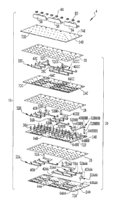
As can be understood from Fig. 5, the conductor apparatus 20 can be said to
include a plurality of conductor assemblies, with the exemplary bus apparatus
4
described herein having nine such conductor assemblies indicated at the
numerals
32A, 32AA, 32AAA, 32B, 32BB, 32BBB, 32BBBB, 32C, and 32CC, and which are
collectively referred to herein with the numeral 32. In the exemplary
embodiment
depicted herein, each such conductor assembly 32 includes a bus element
(described
below) that is embedded within the substrate 16. Each such conductor assembly
32
further include a number of connection elements (described below) that each
have an
electrical connection with the corresponding bus element at a location within
the
interior of the substrate 16 but that also extend from such connection to a
location at
the exterior of the substrate 16. As employed, the expression "a nurnber of'
and
variations thereof shall refer broadly to any non-zero quantity, including a
quantity of
one.
For example, and as can be seen in Fig. 5, the conductor assembly 32A
includes a bus element 40A and a plurality of connection elements 36A that are
electrically connected with the bus element 40A. The conductor assembly 32AA
includes a bus element 40AA and a plurality of connection elements 36A that
are
electrically connected with the bus element 40AA. The conductor assembly 32AAA
includes a bus element 40AAA, and a plurality of connection elements 36A that
are
electrically connected with the bus element 40AAA.
In a similar fashion, the conductor assembly 32B has a bus element 40B to
which is connected a number of the connection elements 36B. The conductor
assembly 32BB has a bus element 4OBB to which is connected a number of the
connection elements 36B. The conductor assembly 32BBB has a bus element
4OBBB to which is connected a number of the connection elements 36B. The
conductor assembly 32BBBB has a bus element 4OBBBB to which is connected a
number of the connection elements 36B.
Likewise, the conductor assembly 32C has a bus element 40C with which are
connected a number of the connection elements 36C. The conductor assembly 32CC
6
CA 02837212 2013-11-22
WO 2012/177826
PCT/US2012/043463
has a bus element 40CC with which are connected a number of the connection
elements 36C.
As can be understood from Fig. 5, the bus elements 40A, 40A A, 40AAA, 40B,
4OBB, 4OBBB, 4OBBBB, 40C, and 40CC, collectively referred to herein at the
numeral 40, are generally thin and fiat and are formed of one of the
electrically
conductive materials mentioned herein or another appropriate material. Such
bus
elements 40 can be formed, for example, by any of a variety of methods such as
laser
cutting, stamping, wire electro-discharge machining, water jet cutting, or
other
appropriate method. The bus elements 40 may be, for example, 0.015 inches in
.. thickness, which may be suitable for a seventy-five Ampere current.
However, other
dimensions can be appropriate for other current-carrying capabilities.
Moreover, the
bus elements 40 can alternatively be of other shapes, such as in the shapes of
wires or
other shapes, without departing from the present concept.
The exemplary connection elements 36A, as well as the other connection
elements mentioned herein, are in the exemplary form of cylindrical pins that
extend
in a direction transverse to the plane of the corresponding bus elements 40A
and 40B.
Shapes other than cylindrical may be employed depending upon the needs of the
application.
The conductor apparatus 20 further includes a plurality of other connectors
which are collectively referred to herein at the numeral 52. One of the other
connectors 52 is connected with each bus element 40 and can be used, for
example, to
electrically connect the bus element 40 with a power source. Such other
connectors
thus are referred to herein as line connectors, although the expression is
intended to
not be limiting since they can be otherwise connected without departing from
the
present concept. As can be seen in Fig. 5, the bus elements 40A, 40AA, 40AAA,
40B, 4OBB, 4OBBB, 4013BBB, 40C, and 40CC each have a line connector 52A,
52AA, 52AAA, 52B, 52BB, 52BBB, 52BBBB, 52C, and 52CC, respectively,
connected therewith. In the exemplary embodiment described herein, the line
connectors 52 each have a threaded end that is cooperable with a nut 60 for
connection with the power source, by way of example. The conductor apparatus
20
further includes a plurality of terminal stops 56 which are disposed on the
substrate 16
in order to facilitate such connection. The terminal stops 56 may potentially
be
7
CA 02837212 2013-11-22
WO 2012/177826
PCT/US2012/043463
mounted on the substrate 16 with the use of some type of an adhesive or
bonding
agent, if desired.
As can further be seen in Fig. 5, at least some of the layers 24ABCD in the
depicted exemplary embodiment have a number of channels formed therein that
are
structured to receive therein the bus elements 40 prior to bonding together of
the
layers 24ABCD to form the substrate 16. In particular, the layer 24A has a
pair of
channels 64A, 64AA, and 64AAA formed therein that are structured to receive
therein
the bus elements 40A, 40AA, and 40AAA. The channels 64A, 64AA, and 64AAA
each include one or more elongated channel segments that are connected
together and
that are sized to accommodate therein the bus elements 40A, 40AA, and 40AAA.
In a
similar fashion, the layer 24B has a set of channels 64B, 64BB, 64BBB, and
64BBBB
formed therein that are structured to accommodate and to receive therein the
bus
elements 40B, 4OBB, 4OBBB, and 4OBBBB. The layer 24C likewise has a pair of
channels 64C and 64CC formed therein to receive the bus elements 40C and 40CC.
As can further be seen in Fig. 5, the layers 24ABCD each have a plurality of
holes formed therein that arc shown generally at the numerals 72A, 72B, 72C,
and
72D, respectively, and which are positioned and sized to accommodate therein
at least
a portion of each of the connection elements 36ABCD. For example, the layer
24A
has a plurality of holes 72A formed therein, the layer 24B has a plurality of
holes 72B
formed therein, the layer 24C has a plurality of holes 72C formed therein, and
the
layer 24D has a plurality of holes 721) formed therein. The holes 72A receive
the
connection elements 36A therein. It can likewise be said that the holes 72B
receive
the connection elements 36B therein, that the holes 72C receive the connection
elements 36C therein, and the holes 720 receive the connection elements 36D
therein.
It is noted, however, that the holes 72ABCD are generally aligned with one
another
when the substrate 16 is assembled, and it therefore can be seen that certain
of the
connection elements 36ABCD are each received through the holes 72ABCD in more
than one of the layers 24ABCD. For example, the connection elements 36D are
each
received in the holes 72ABCD and moreover extend to a region exterior to the
substrate 16. For instance, the substrate 16 can be said to have a pair of
generally
planar surfaces 74A and 74B. The connection elements 361) each have a first
end 80
8
CA 02837212 2013-11-22
WO 2012/177826
PCT/US2012/043463
that protrudes beyond the surface 74A and further include a second end 82 that
protrudes beyond the surface 74B.
In a similar fashion, the connection elements 36ABC each have a first end 78
that protrudes outwardly from the surface 74A. In order to enable the
connection
elements 36ABC to generally each protrude outwardly from the surface 74A in a
fashion similar to the connection elements 38D, certain of the connection
elements, in
particular the connection elements 36B and 36C, must extend through the holes
74AB
formed in more than one of the layers. For example, the connection elements
36B
must extend through both the holes 72B formed in the layer 24B as well as the
holes
72A formed in the layer 24A. Likewise, the connection elements 36C must extend
not only through the holes 72C, but also through the holes 72B and the holes
72A in
order to protrude outwardly from the surface 74A.
It is noted, however, that the bus elements 40A, 40AA, 40AAA, 40B, 40B B,
4OBBB, 4OBBBB, 40C, and 40CC are each electrically isolated from one another.
The bus elements 40 are also each electrically isolated from the connection
elements
36D within the interior of the substrate 16. The of bus elements 40 situated
between
the various adjacent pairs of layers 24ABCD may be connected with any of a
variety
of power sources, by way of example, with each such bus element 40 remaining
isolated from each other bus element 40.
For instance, any of the bus elements 40 can carry AC or DC power at any of a
wide range of voltages and current levels, as long as the various
specifications of the
conductor apparatus 20 are suited to carry such power. Also, the geometry is
scalable
to enable larger quantities of connections to be made, and the substrate 16
can itself
be made physically larger in each dimension depending upon the specific needs
of the
particular application.
By way of example and without limitation, the conductor assemblies 32A,
32B, and 32C are connected with the three phases of a three-phase AC
electrical
system, and the conductor assemblies 32AA, 32BB, and 32CC are connected with
the
three phases of a separate three-phase AC electrical system. The conductor
assemblies 32AAA and 32BBB arc each connected with separate AC electrical
lines,
and the conductor assembly 32BBBB is connected with DC power. It thus is
9
CA 02837212 2013-11-22
WO 2012/177826
PCT/US2012/043463
understood that the bus apparatus 4 can be connected with virtually any type
of power
system and can be configured to meet any of a variety of electrical connection
needs.
In the depicted exemplary embodiment, and as mentioned above, the substrate
16 is formed by stacking the layers 24ABCD and alternating them with layers of
the
bonding material 28. In the exemplary embodiment depicted herein, the bonding
Material 28 is in the form of thin sheets which may be on the order of 0.005
inches in
thickness and which are formed with holes that correspond with the holes
72ABCD..
When the bus elements 40 are received in the channels 64, and when the bonding
material 28 is interposed between the adjacent pairs of the layers 24AB, 24BC,
and
24CD, and when the connection elements 36D are installed, in the holes 72ABCD,
the
components of the substrate 16 will be in a condition stacked and aligned with
one
= another and will be ready for final assembly.
In particular, the stacked elements of the substrate 16 are situated in a
curing
machine 84, a portion of which is indicated in Fig. 7, and which includes a
first mold
portion 86 and a second mold portion 88 that are configured to be compressed
together as shown with the arrows that are indicated generally at the numerals
92A
and 92B. In particular, the stacked elements of the substrate 16 prior to
curing are
situated between the first and second mold portions 86 and 88, and the curing
machine 84 is caused to compress together the first and second mold portions
86 and
88 and to apply heat thereto, which results in compression and temperature
above
ambien.t conditions being applied to the substrate 16. By way of example, the
elements of the substrate can be heated to a temperature on the order of 200
degrees
Fahrenheit and a pressure on the order of, for example, 100 to 2000 psi
pressure for a
period of one or two hours. Other temperatures, pressures, and durations can
be
employed without departing from the present concept.
The application of such temperature and pressure causes the substrate 16 to
cure, meaning that the bonding material 28 may transfer epoxy and become cross-
linked with the adjacent layers 24ABCD. The result of the curing process may
vary
depending upon the specific characteristics of the bonding material 28. During
such
curing, the bonding material 28 may additionally cause epoxy to flow around at
least
a portion of the bus elements 40, as well as at least a portion of the
connection
elements 36ABCD, which provides a desirable dielectric and moisture barrier
=
CA 02837212 2013-11-22
WO 2012/177826
PCT/US2012/043463
between the layers 24ABCD and which results in the bus elements 40 being
embedded within the substrate 16.
It thus is understood that in other embodiments the bus apparatus 3
potentially
may be configured without the channels 64. That is, the layers 24ABCD may
simply
be formed with planar surfaces and the bus elements 40 received thereon. By
providing a relatively greater amount of the bonding material 28, and with
curing,
such additional amounts of bonding material 28 could flow into the vicinity
around
each bus element 40 and occupy the space between each adjacent layer 24ABCD
that
is not occupied by one of the bus elements 40.
After the predetermined duration of time in the curing machine 84 with the
aforementioned heat and pressure, the first and second mold portions 86 and 88
are
separated from one another, and the completed bus apparatus 4 with the cured
substrate 16 is removed from the curing machine 84. The layers 24ABCD may each
be on the order of 0.060 inches in thickness, with the result that the
completed
substrate 16 is on the order of one-quarter inch in thickness.
The substrate 16 is generally rigid and is strong enough to accommodate
connections of circuit interrupters such as the circuit interrupter 8 with
pairs of the
connection elements 36ABCD. That is, the connection elements 36ABCD in the
depicted exemplary embodiment can be said to be arranged in pairs 90ABC for
.. connection with a device such as thc circuit interrupter 8. For example, a
pair 90A as
is depicted generally in Fig. 1 includes a first end 78 of one of the
connection
elements 36A and a first end 80 of one of the connection elements 36D. A pair
90B
includes a first end 78 of one of the connection elements 36B and a first end
80 of one
of the connection elements 36D. Likewise, a pair 90C includes a first end 78
of a
.. connection element 36C and a first end 80 of a connection element 36D. The
connection elements 36D can be employed, as suggested above, for connection
with
loads such as the load 12. It thus can be understood that each of the pairs
90ABC
includes a connection element that can be connected with a line, such as one
of the
connection elements 36A or one of the connection elements 36B or one of the
.. connection elements 36C, and further includes one of the connection
elements 36D
that can be connected with a load. Depending upon the particular application,
a
circuit interrupter may be a multi-phase circuit interrupter that will be
connected with
11
CA 02837212 2013-11-22
WO 2012/177826
PCT/US2012/043463
more than one of the pairs 90ABC. For example, a three-phase circuit
interrupter
might be connected with three pairs, i.e., a pair 90A, a pair 90B, and a pair
90C,
which likely would be situated adjacent one another. Other variations will be
apparent.
Fig, 6 depicts a flowchart which sets forth certain of the operations that are
performed in assembling and curing the substrate 16. In particular, each of
the
conductor assemblies 32 is positioned, as at 106, with the bus elements 40
received in
the channels 64 and with the connection elements 36A13C which, in the depicted
exemplary embodiment, are line connection elements, received in the holes
72ABC.
The connection elements 36D which, in the depicted exemplary embodiment are
load
connection elements, are received in the holes 7213, as at 110. In this
regard, it can be
seen that each of the exemplary connection elements 36D includes an annular
flange
at generally the midpoint thereof that engages at least the layer 24B and
serves as a
support element. Such annular flange helps to secure the connection elements
36D to
the substrate 16 and to resist unintended extraction of the connection
elements 36D
from the substrate 16 during insertion and removal of circuit interrupters 8
and loads
12. Moreover, it is noted that the connection elements 36ABC likewise each
include
an annular flange which serves as a support element and which helps to secure
such
= connection elements 36ABC against unintended separation from the cured
substrate
16.
The bonding material 28 is then positioned between adjacent pairs of the
layers 24ABCD, as at 114, so that the layers 24ABCD and the bonding material
28
are aligned and stacked. The aligned and stacked layers 24A13C1) and bonding
material 28 with the conductor apparatus 20 installed thereon are then
positioned, as
at 118, in the curing machine 84. The uncured substrate 16 is then subjected,
as at
122, to compression and heating for a predetermined period of time. The
completed
bus apparatus 4 with its cured substrate 16 is then removed, as at 126, from
the curing
machine 84.
The completed bus apparatus 4 thus enables lines to be connected with the line
connectors 52 and allows loads to be connected with the second ends 82 of the
connection elements 36D, and further permits circuit interrupters, such as the
circuit
interrupter 8, to be electrically interposed therebetwcen by connecting them
across
12
CA 02837212 2013-11-22
WO 2012/177826
PCT/US2012/043463
pairs 90A13C of the first ends 78 and 80. Various arrangements of the
conductor
apparatus 20 can be provided depending upon the needs of the particular
application.
The resultant cured substrate 16 provides to the bus apparatus a direct
thermal route
for dissipation of 12R heat while maintaining electrical isolation between the
various
conductor assemblies 32, as well as isolation from the connection elements 36D
within the substrate. The bus apparatus 4 thus enables a variety of
connections to be
made between lines and loads and eliminates the need for the extensive wiring
that
had been used with previous systems. In this regard, while only a single load
12 is
depicted as being connected with a single connection element 36D, it is
understood
that a board (not expressly depicted herein) can be proved with connectors
disposed
thereon that are electrically connected with the various loads of the
application, and
the board can be connected with the various appropriate second ends 82 of the
connection elements 36D. Other variations will be apparent to one of ordinary
skill in
the art.
An alternative bus apparatus 204 in accordance with a second embodiment of
the disclosed and claimed concept is depicted generally in Figs. 8-11. The bus
apparatus 204 is similar to the bus apparatus 4 in that the bus apparatus 204
includes a
substrate 216 having a plurality of layers 224ABCD and further comprises a
conductor apparatus 220 having a plurality of conductor assemblies 232 'having
bus
elements and connection elements 236ABC.
The bus apparatus 204 is different from the bus apparatus 4 in that the
connection elements 23613 of the conductor apparatus 220 are electrically
connected,
such as through soldering or welding, with a printed circuit board 294. For
example,
the connection elements 236D are soldered to appropriate locations on the
printed
circuit board 294, and the connection elements 236 are then received in holes
272A13CD in the layers 224ABCD. In so doing, a layer of bonding material 228
is
interposed between the layer 224D and the printed circuit board 294. As such,
curing
of the substrate 216 together with the printed circuit board in a curing
machine
configured to accommodate them causes the printed circuit board 294 to be
bonded
together with the substrate 216 upon curing. It is noted that electrical
connections can
be made herein by any appropriate methodology, including via mechanical
stress,
brazing, riveting, and the use of electrical connectors, by way of example.
13
CA 02837212 2013-11-22
WO 2012/177826
PCT/US2012/043463
The printed circuit board 294 has a connector 296 which includes pins or other
connectors that can be connected with the various loads. The connector 296
also
includes other pins or other connectors that provide one or more data channels
which
communicate to a remote location data derived by circuits situated on the
printed
circuit board 294.
While the printed circuit board 294 is depicted herein as being engaged with
the layer 2241) with the layer of bonding material 228 situated therebetween
and with
the elements then being cured together, it is noted that the installation of
the printed
circuit board 294 with the connection elements 236B soldered thereto can be
performed after curing of the substrate 216. Other variations will be
apparent.
The addition of the printed circuit board 294 thus enables the generation of
data regarding the various circuits with which the bus apparatus 204 is
connected and
the delivery of such data to remote a location. Such data can include
condition data,
such as ON or OFF conditions of each circuit (and thus the circuit
interrupter), as well
as voltage and current levels and the like on each circuit, which is
desirable. Other
variations will be apparent.
While specific embodiments of the invention have been described in detail, it
will be appreciated by those skilled in the art that various modifications and
alternatives to those details could be developed in light of the overall
teachings of the
disclosure. Accordingly, the particular arrangements disclosed are meant to be
illustrative only and not limiting as to the scope of invention which is to be
given the
full breadth of the claims appended and any and all equivalents thereof.
14