Note: Descriptions are shown in the official language in which they were submitted.
CA 02837555 2013-11-27
WO 2012/167085 PCT/US2012/040468
PHOTOVOLTAIC MODULE ASSEMBLY AND METHOD OF
ASSEMBLING THE SAME
CROSS-REFERENCE TO RELATED APPLICATIONS
100011 The subject patent application claims priority to and all the benefits
of U.S. Provisional
Patent Application No. 61/492,674 filed June 2, 2011; U.S. Provisional Patent
Application No.
61/492,694 filed June 2, 2011; U.S. Provisional Patent Application No.
61/524,688 filed August
17, 2011; and U.S. Provisional Patent Application No. 61/524,661 filed August
17, 2011, each
of which are incorporated herein by reference.
BACKGROUND OF THE INVENTION
1. Field of the Invention
[0002] The present invention includes a photovoltaic module assembly, and
specifically, a
photovoltaic module assembly including a photovoltaic module including at
least one crystalline
silicon photovoltaic cell, a rail mounted to the photovoltaic module, and an
adhesive formed
from a room-temperature vulcanizing silicone composition and adhering the rail
the photovoltaic
module. The present invention also includes a method of assembling the same.
2. Description of the Related Art
[0003] A photovoltaic module includes a photovoltaic cell that converts
sunlight into electricity.
A plurality of photovoltaic modules are typically connected together at a
photovoltaic module
installation site such as a solar field, e.g., for large-scale commercial
energy production, a roof
top of building, a side of a building, etc. The photovoltaic module
installation site includes a
racking system for supporting the plurality of photovoltaic cells.
[0004] The photovoltaic module is assembled into a photovoltaic module
assembly for
mounting to the racking system. Specifically, the photovoltaic module is
combined with a frame,
a rail, or a pad that is suitable to engage the racking system to mount the
photovoltaic module
assembly on the racking system.
SUMMARY OF THE INVENTION AND ADVANTAGES
[0005] The present method includes a photovoltaic module assembly for mounting
on a frame of
a racking system of a photovoltaic module installation site. The photovoltaic
module assembly
comprises at least one photovoltaic module including a back sheet, at least
one crystalline silicon
photovoltaic cell supported on the back sheet, a first encapsulant layer
formed from a silicone
composition supported on the photovoltaic cell, and a cover sheet supported on
the first
encapsulant layer. At least one rail is fixed relative to the back sheet. The
rail is configured to
support the at least one photovoltaic module on the racking system of the
photovoltaic module
installation site. Adhesive is disposed between and contacts the back sheet of
the at least one
1
CA 02837555 2013-11-27
WO 2012/167085 PCT/US2012/040468
photovoltaic module and the at least one rail to adhere the at least one rail
to the at least one
photovoltaic module. The adhesive is formed from a room-temperature
vulcanizing silicone
composition. The adhesive has a thickness from the rail to the back sheet of
between 2.3mm and
6.0mm.
[0006] The invention also includes a method of assembling a photovoltaic
module assembly.
The method comprises providing at least one photovoltaic module including at
least one
crystalline silicon photovoltaic cell, a first encapsulant layer formed from a
silicone composition
disposed on the photovoltaic cell, and a cover sheet disposed on the first
encapsulant layer. The
method comprises providing at least one rail. The method comprises applying a
room-
temperature vulcanizing silicone composition to one of the back sheet or the
rail. The method
comprises contacting the room-temperature vulcanizing silicone composition to
the other of the
back sheet or the rail. And the method comprises curing the room-temperature
vulcanizing
silicone composition while in contact with the back sheet and the rail to
adhere the rail to the
back sheet. The step of applying the room temperature vulcanizing silicone
composition
includes applying the room temperature vulcanizing silicone composition at a
thickness such
that the room-temperature vulcanizing silicone composition cures into an
adhesive adhering the
rail to the back sheet and having a thickness from the rail to the back sheet
of between 2.3mm
and 6.0rnm.
BRIEF DESCRIPTION OF THE DRAWINGS
[0007] Other advantages of the present invention will be readily appreciated,
as the same
becomes better understood by reference to the following detailed description
when considered in
connection with the accompanying drawings wherein:
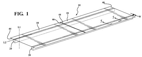
[0008] Figure 1 is a perspective view of a photovoltaic module assembly;
[0009] Figure 2 is a perspective view of another photovoltaic module assembly;
[0010] Figure 3 is a perspective view of another photovoltaic module assembly;
[0011] Figure 4 is a perspective view of another photovoltaic module assembly;
[0012] Figure 5 is a cross-sectional view of a portion of the photovoltaic
module assembly
through line 5 of Figure 1; and
[0013] Figure 6 is a perspective view of a racking system of a photovoltaic
module installation
site and a plurality of photovoltaic module assemblies mounted on the racking
system.
DETAILED DESCRIPTION OF THE INVENTION
100141 Referring to the Figures, wherein like numerals indicate like parts
throughout the several
views, a photovoltaic module assembly 10 is generally shown in Figures 1-4.
With reference to
2
CA 02837555 2013-11-27
WO 2012/167085 PCT/US2012/040468
Figure 6, the photovoltaic module assembly 10 is supported on a frame 12 of a
racking system
14 of a photovoltaic module 18 installation site 16. Specifically, the
photovoltaic module=
assembly 10 includes at least one photovoltaic module 18 and at least one rail
20 mounted to the
photovoltaic module 18 for engaging the frame 12. The photovoltaic module
assembly 10, also
referred to in industry as a solar cell module assembly, converts sunlight
into electricity.
Typically various components such as inverters, batteries, wiring, etc., are
connected to the
photovoltaic module assembly 10 and are not shown in the Figures for the sake
of drawing
clarity. The photovoltaic module 18 installation site 16 can, for example, be
a solar field, e.g.,
for large-scale commercial energy production, a roof top of building, a side
of a building, etc.
[0015] The rail 20 is typically engaged with the racking system 14 to support
the photovoltaic
module assembly 10 on the racking system 14 and can be engaged with the
racking system 14 in
any suitable fashion without departing from the nature of the present
invention. The rail 20 can
be formed of any type of material such as, for example, galvanized steel,
aluminum, etc.
[0016] The at least one photovoltaic module 18 can be further defined as a
plurality of
photovoltaic modules 18. In other words, the photovoltaic module assembly 10
can include a
plurality of photovoltaic modules 18, i.e., typically referred to in industry
as a multi-module
panel.
[0017] The at least one rail 20 can be further defined as a plurality of rails
20. The photovoltaic
module assemblies 18 shown in Figures 1 and 3 include two rails 20 and two
photovoltaic
modules 18 and the photovoltaic module assemblies 18 shown in Figures 2 and 4
include two
rails and one photovoltaic module 18. The photovoltaic module assembly 10 of
Figure 6
includes five photovoltaic modules 118. The photovoltaic module assembly 10
can include any
number of rails 20, i.e., one or more rails 20, and any number of photovoltaic
modules 18, i.e.,
one or more photovoltaic modules 18, without departing from the nature of the
present
invention. When the photovoltaic module assembly 10 includes a plurality of
photovoltaic
modules 18, each of the photovoltaic modules 18 of the assembly 10 are
physically connected to
each other via the rail 20 and are also typically electrically connected to
each other.
[0018] Typically, the rail 20 is connected to the photovoltaic modules 18 only
with adhesive 30,
as set forth further below, i.e., the photovoltaic module assembly 10 is
frameless. The rail 20 is
adhesively secured to the photovoltaic modules 18 and the adhesive 30 acts as
a structural
adhesive that supports the at least one photovoltaic module 18 on the at least
one rail 20. The
attachment of the rails 20 to the photovoltaic modules 18 is typically free of
any type of
mechanical hardware such as fasteners and clamps that clamp the rail 20 onto
the photovoltaic
module 18, i.e., the rails 20 typically are not mechanically fastened to the
photovoltaic modules
3
CA 02837555 2013-11-27
. WO 2012/167085 PCT/US2012/040468
18. As such, the material and assembly costs associated with such mechanical
hardware or
fasteners are eliminated and the handling of the fragile photovoltaic modules
18 by workers
associated with assembling mechanical hardware or fasteners is eliminated. In
addition, damage
to the photovoltaic modules 18 caused by over-tightening of the mechanical
hardware is
eliminated. Also, the adhesive 30 is a theft deterrent because it is
relatively difficult to break the
adhesive 30 between the rail 20 and the photovoltaic module 18 without proper
tools.
100191 With reference to Figure 5, the photovoltaic module 18 includes a back
sheet 32, at least
one photovoltaic cell 34 supported on the back sheet 32, a first encapsulant
layer 36 formed
from a silicone composition supported on the photovoltaic cell 34, and a cover
sheet 38
supported on the first encapsulant layer 36. =
(00201 The at least one photovoltaic cell 34 is disposed between the back
sheet 32 and the cover
sheet 38. The photovoltaic module 18 may include one photovoltaic cell 34 or a
plurality of
photovoltaic cells 34. Typically, the photovoltaic module 18 includes a
plurality of photovoltaic
cells 34. When the photovoltaic module 18 includes the plurality of the
photovoltaic cells 34, the
photovoltaic cells 34 may be substantially coplanar with one another.
Alternatively, the
photovoltaic cells 34 may be offset from one another, such as in non-planar
module
configurations. Regardless of whether the photovoltaic cells 34 are planar or
non-planar with
one another, the photovoltaic cells 34 may be arranged in various patterns,
such as in a grid-like
pattern.
100211 The photovoltaic cells 34 may independently have various dimensions, be
of various
types, and be formed from various materials. The photovoltaic cells 34 may
have various
thicknesses, such as from about 50 to about 250, alternatively from about 100
to about 225,
alternatively from about 175 to about 225, alternatively about 180,
micrometers (gm) on
average. The photovoltaic cells 34 may have various widths and lengths. In one
embodiment, the
photovoltaic cells 34 are crystalline silicon photovoltaic cells 34 and
independently comprise
monocrystalline silicon, polycrystalline silicon, or combinations thereof.
100221 When the photovoltaic module 18 includes more than one photovoltaic
cell 34, a tabbing
ribbon is typically disposed between adjacent photovoltaic cells 34 for
establishing a circuit in
the photovoltaic module 18.
[00231 The back sheet 32 can be formed from various materials. Examples of
suitable materials
include glass, polymeric materials, composite materials, etc. For example, the
back sheet 32 can
be formed from glass, polyethylene terephthalate (PET), thermoplastic
elastomer (TPE),
polyvinyl fluoride (PVF), silicone, etc. The back sheet 32 may be formed from
a combination of
different materials, e.g. a polymeric material and a fibrous material. The
back sheet 32 may have
4
CA 02837555 2013-11-27
WO 2012/167085 PCT/US2012/040468
portions formed from one material, e.g. glass, and other portions formed from
another material,
e.g. a polymeric material. The back sheet 32 can be of various thicknesses,
such as from about
0.05 to about 5, about 0.1 to about 4, or about 0.125 to about 3.2,
millimeters (mm) on average.
Thickness of the back sheet 32 may be uniform or may vary.
[0024] Further examples of suitable back sheets 32 include those described in
U.S. App. Pub.
Nos. 2008/0276983, 2011/0005066, and 2011/0061724, and in WO Pub. Nos.
2010/051355 and
2010/141697, the disclosures of which are incorporated herein by reference in
their entirety to
the extent they do not conflict with the general scope of the disclosure. The
aforementioned
disclosures are hereinafter referred to as the "incorporated references."
[0025] The cover sheet 38 may be substantially planar or non-planar. The cover
sheet 38 is
useful for protecting the module 18 from environmental conditions such as
rain, snow, dirt, heat,
etc. Typically, the cover sheet 38 is optically transparent. The cover sheet
38 is generally the sun
side or front side of the module.
[0026] The cover sheet 38 can be formed from various materials. Examples of
suitable materials
include those described above with description of the back sheet 32. Further
examples of
suitable cover sheets 38 include those described in the references
incorporated above. In certain
embodiments, the cover sheet 38 is formed from glass. Various types of glass
can be utilized
such as silica glass, polymeric glass, etc. The cover sheet 38 may be formed
from a combination
of different materials. The cover sheet 38 may have portions formed from one
material, e.g.
glass, and other portions formed from another material, e.g. a polymeric
material. The cover
sheet 38 may be the same as or different from the back sheet 32. For example,
both the cover
sheet 38 and the back sheet 32 may be formed from glass with equal or
differing thicknesses.
[0027] The cover sheet 38 can be of various thicknesses, such as from about
0.5 to about 10,
about 1 to about 7.5, about 2.5 to about 5, or about 3, millimeters (mm), on
average. Thickness
of the cover sheet 38 may be uniform or may vary.
[0028] The first encapsulant layer 36 is disposed on the photovoltaic cells 34
and serves to
protect the photovoltaic cells 34. Further, the first encapsulant layer 36 is
utilized to bond the
photovoltaic module 18 together by being sandwiched between the back sheet 32
(along with the
photovoltaic cells 34) and the cover sheet 38. In particular, the first
encapsulant layer 36 is
generally utilized for coupling the cover sheet 38 to the back sheet 32.
[0029] The silicone composition is typically disposed on the back sheet 32
(along with the
photovoltaic cells 34) to form a first layer. The cover sheet 38 is then
disposed on the first layer,
and the first layer is cured to form the first encapsulant layer 36.
CA 02837555 2013-11-27
WO 2012/167085 PCT/US2012/040468
10030] In various embodiments, the photovoltaic module 18 further includes a
second
encapsulant layer 40 disposed between the back sheet 32 and the photovoltaic
cells 34. In
particular, the second encapsulant layer 40 is for coupling the photovoltaic
cells 34 to the back
sheet 32. The second encapsulant layer 40 generally protects the photovoltaic
cells 34 from the
back sheet 32 because the second encapsulant layer 40 is sandwiched between
the photovoltaic
cells 34 and the back sheet 32. The second encapsulant layer 40 may be
uniformly disposed
across the back sheet 32, or merely disposed between the photovoltaic cells 34
and the back
sheet 32, in which case the second encapsulant layer 40 is not a continuous
layer across the back
sheet 32, but rather is a patterned layer.
10031] The second encapsulant layer 40 may be the same as or different from
the first
encapsulant layer 36. When the first and second encapsulant layers 36,40 are
the same, the first
and second encapsulant layers 40 typically form a continuous encapsulant layer
that
encapsulates the photovoltaic cells 34 between the back sheet 32 and the cover
sheet 38. When
the second encapsulant layer 40 is different from the first encapsulant layer
36, the second
encapsulant layer 40 may only be present between the photovoltaic cells 34 and
the back sheet
32, in which case the second encapsulant layer 40 is not a continuous layer
across the back sheet
32, as noted above. In such embodiments, the first encapsulant layer 36
generally contacts both
the back sheet 32 and the cover sheet 38 in locations in the photovoltaic
module 18 other than
where the photovoltaic cells 34 are disposed.
[0032] Most typically, both the first and the second encapsulant layers 36, 40
are independently
formed from silicone compositions. In such embodiments, the silicone
composition utilized to
form the second encapsulant layer 40 is uniformly applied on the back sheet 32
to form a second
layer, which may optionally be partially or fully cured prior to disposing the
photovoltaic cells
34 on the second layer. The silicone composition utilized to form the first
encapsulant layer 36 is
then applied on the second layer and the photovoltaic cells 34 to form the
first layer. The cover
sheet 38 is applied on the first layer to form a package, and the first and
second layers of the
package are cured to form the first and second encapsulant layers 40 and the
module.
[0033] Although the first encapsulant layer 36 is typically sandwiched between
the back sheet
32 (along with the photovoltaic cells 34) and the cover sheet 38, there may be
at least one
intervening layer between the first encapsulant layer 36 and the cover sheet
38 and/or between
the first encapsulant layer 36 and the photovoltaic cells 34.
[0034] The first encapsulant layer 36 is formed from a silicone composition.
Examples of
silicone compositions suitable for forming the first encapsulant layer 36
include hydrosilylation-
reaction curable silicone compositions, condensation-reaction curable silicone
compositions, and
6
CA 02837555 2013-11-27
WO 2012/167085 PCT/US2012/040468
hydrosilylation/condensation-reaction curable silicone compositions. As noted
above, in certain
embodiments, the second encapsulant layer 40, when present in the photovoltaic
module 18, also
is formed from a silicone composition. The silicone composition utilized to
form the second
encapsulant layer 40 may independently be selected from any of these
compositions.
[0035] The photovoltaic modules 18 are typically 1.0-1.7m wide and 0.6-1.1m
tall, however, the
photovoltaic modules 18 can be of any size. The photovoltaic modules 18 can be
mounted to the
racking system 14 in a landscape orientation, as shown in Figure 6, or in a
portrait orientation.
The rails 20 typically extend longitudinally across the upper and lower
mounting bars 42 of the
racking system 14. As such, the photovoltaic module assembly 10 shown in
Figures 1 and 2, for
example, are configured to be mounted to the racking system 14 in the portrait
orientation and
the photovoltaic module assembly 10 shown in Figures 3 and 4, for example, are
configured to
be mounted to the racking system 14 in a landscape orientation. Alternatively,
the photovoltaic
module 18 can be mounted to the racking system 14 in any orientation without
departing from
the nature of the present invention.
[0036] As set forth above, the photovoltaic module assembly 10 includes at
least one rail 20
mounted to the photovoltaic module 18. Specifically, as set forth further
below, the rail 20 is
fixed relative to the back sheet 38 of the photovoltaic module 18. The rail 18
is adhered to the
back sheet 32 with the adhesive 30, as set forth further below.
[00371 The rail 20 is configured to support the photovoltaic module assembly
18 on the frame
12 of the racking system 14 of the photovoltaic module installation site 16.
For example, the rail
20 can include a hook (not shown) sized and shaped to engage the racking
system 14. In
addition to or in the alternative to the hook, fasteners (not shown) typically
secure the rail 20 to
the racking system 14.
[0038] With reference to Figures 1-4, the back sheet 32 of the at least one
photovoltaic module
18 includes a first end 44 and a second end 46. In other words, the
photovoltaic module 18
terminates at the first end 44 and the second end 46. The at least one rail 20
continuously
extends across the back sheet 32 from the first end 44 to the second end 46.
Said differently, the
at least one rail 20 extends to or crosses the perimeter of the back sheet 32
at the first end 44 and
the second end 46. Alternatively, the at least on rail 20 can be spaced from
the perimeter at the
first end 44 and the second end 46. In any event, the back sheet 32 defines a
length L between
the first end 44 and the second end 46 and the at least one rail 20 extends
across the back sheet
32 continuously and along substantially the length L of the back sheet 32.
[0039] As set forth above, the at least one rail 20 is adhered to the back
sheet 32 of the at least
one photovoltaic module 18 with the adhesive 30. The adhesive 30 is disposed
between and
7
CA 02837555 2013-11-27
WO 2012/167085 PCT/US2012/040468
contacts the at least one photovoltaic module 18 and the at least one rail 20.
The adhesive 30
fixes the photovoltaic module 18 and the rail 20 together as a unit.
100401 While the photovoltaic module assembly 10 is mounted to the frame 12 of
the racking
system 14, photovoltaic module assembly 10 and the frame 12 undergo thermal
expansion and
retraction resulting in relative movement between the photovoltaic module
assembly 10 and the
frame 12 that imposes shear stress upon the adhesive 30. The amount of
movement between the
photovoltaic module assembly 10 and the frame 12 depends on the materials and
the
temperature change.
[0041] The adhesive 30 has a thickness T from the rail 20 to the back sheet 32
and a width W
between the rail 20 and the back sheet 32. The minimum magnitude for the
thickness T and the
width W are calculated as discussed below. With reference to Figure 1, the
thickness T is
measured along a first line LI extending from the at least one rail 20 to the
back sheet 32. The
width W is measured along a second line L2 perpendicular to the first line Ll
. Specifically, the
rail 20 and the back sheet 32 define planar surfaces 48 and the first line Li
extends
perpendicularly to the planar surfaces 48 of the rail 20 and the back sheet 32
as shown in Figure
5.
[0042] The thickness T is at a minimal magnitude to accommodate for the
thermal expansion
and retraction. The minimal magnitude for the thickness T can be calculated
with the following
formula:
Thermal Expansion (m)xYoung Modulus of Adhesive (Pa)
Min.Joint Thickness (n) =
3xMaxintum Allowable Stress in Shear (Pa)
In this calculation, the maximum allowable stress in shear is determined by
Ru,5 value as
determined in shear. In any event, with the use of this calculation, the
thickness T of the
adhesive is typically between 2.3mm and 6.0mm. In other words, the minimum
joint thickness is
typically between 2.3mm and 6.0mm.
[0043] The width W is at a minimum magnitude to withstand wind load. The width
W of the
adhesive 30 to withstand a given wind, i.e., the minimal structural bite for
wind load, is directly
proportional to the wind load on the photovoltaic module assembly 10 and the
dimensions of the
photovoltaic module 18. Test standards are set forth by the International
Electrotechnical
Commision (IEC) for testing wind loads such as, for example, IEC 61215 and IEC
61646. The
minimum structural bite can be calculated with the following formula:
Back Sheet Area (m2) X Wind Load (Pa)
Min. Structural Bite(m) = ____________________________________________________
Bond Length (m) x Maximum Allowable Design Stress (Pa)
8
CA 02837555 2013-11-27
WO 2012/167085 PCT/US2012/040468
In this calculation, the maximum allowable design stress is based on the Ru,5
value with a safety
factor of 6. The Ru,5 value is the probability at 75% that 95% of the
population will have a
breakage strength above this value. In any event, with the use of this
calculation, the width W is
typically between 5mm and 20mm. In other words, the minimum structural bite is
typically
between 5mm and 20mm.
(0044] Further, if the photovoltaic module assembly 10 is to be qualified to
withstand heavy
accumulations of snow and ice, the load applied to the photovoltaic module
assembly 10 is
increased for mechanical load tests under IEC 61215 and 1EC 61646. In such an
embodiment,
the minimum width W can be calculated using the following calculation for
minimum structural
bite for dead load:
in
Module Mass X 9.81 ¨2.
Min. Structural Bite (in) = ________________________________________________
Bond Length x Allowable Design DL Stress (Pa)
In this calculation, the allowable design DL (dead load) stress is dependent
upon the type of the
adhesive 30.
[0045] The adhesive 30 can be any type of adhesive. For example, in certain
embodiments, the
adhesive 30 is formed from a silicone composition such that, once cured (or
even prior to
curing), the adhesive 30 comprises a silicone. The adhesive 30 advantageously
has excellent
adhesion to glass and metals, as well as a variety of other materials and
substrates. The adhesive
30 is also flexible so as to absorb mismatches caused by differences in
coefficient of thermal
expansion of different material and to reduce stress on the photovoltaic
module 18. The adhesive
30 can also withstand wind load and snow load and adequately resists
deterioration.
[0046] The silicone composition utilized to form the adhesive 30 may comprise
any type of
silicone composition suitable for forming the adhesive 30. For example, in
various
embodiments, the silicone composition is selected from the group of a
hydrosilylation-reaction
curable silicone composition, a peroxide-curable silicone composition, a
condensation-curable
silicone composition, an epoxy-curable silicone composition, an ultraviolet
radiation-curable
silicone composition, and a high-energy radiation-curable silicone
composition.
[0047] In one specific embodiment, the silicone composition used to form the
adhesive 30
comprises a room-temperature vulcanizing silicone composition, which typically
is either a
hydrosilylation-reaction curable silicone composition or a condensation-
curable silicone
composition. Such room-temperature vulcanizing silicone composition are
desirable because the
adhesive 30 may be formed from these room-temperature vulcanizing silicone
compositions
without necessitating certain curing conditions associated with many silicone
compositions, e.g.
9
=
CA 02837555 2013-11-27
WO 2012/167085 PCT/US2012/040468
the application of heat. Accordingly, room-temperature vulcanizing silicone
compositions may
be utilized to form the adhesive 30 in a variety of locations, e.g. outdoors,
in a variety of
conditions. For example, the room-temperature vulcanizing silicone
compositions may be
utilized where assembly of the mounting rails 20 to the photovoltaic module 18
often takes place
without necessitating, for example, a curing oven or other heat source for
curing the silicone
composition. While room-temperature vulcanizing silicone compositions may cure
at ambient
conditions, curing of such room-temperature vulcanizing silicone compositions
may be
accelerated via the application of heat, if desired.
[0048] When the silicone composition comprises the room-temperature
vulcanizing silicone
composition that is hydrosilylation-reaction curable, the silicone composition
typically
comprises an organopolysiloxane having at least two silicon-bonded alkenyl
groups and an
organosilicon compound having at least two silicon-bonded hydrogen atoms. The
organopolysiloxane and the organosilicon compound may independently be
monomeric,
oligomeric, polymeric, or resinous, and may independently comprise any
combination of M, D,
T, and/or Q units depending upon the desired physical properties of the
adhesive 30. The silicon-
bonded alkenyl groups of the organopolysiloxane and the silicon-bonded
hydrogen atoms of the
organosilicon compound may independently be pendent, terminal, or both.
Further, additional
non-reactive compounds, such as a non-reactive polyorganosiloxane, may be
present in the
silicone composition. The reaction between the organopolysiloxane and the
organosilicon
compound is typically catalyzed by a hydrosilylation-reaction catalyst. The
hydrosilylation-
reaction catalyst can be any of the well-known hydrosilylation catalysts
comprising a platinum
group metal (i.e., platinum, rhodium, ruthenium, palladium, osmium and
iridium) or a
compound containing a platinum group metal. Preferably, the platinum group
metal is platinum,
based on its high activity in hydrosilylation reactions.
[0049] Hydrosilylation-reaction catalysts include the complexes of
chloroplatinic acid and
certain vinyl-containing organosiloxanes disclosed in U.S. Pat. No. 3,419,593,
which is hereby
incorporated by reference in its entirety. A catalyst of this type is the
reaction product of
chloroplatinic acid and 1,3-d ietheny1-1,1,3,3-tetramethyldisiloxane.
[0050] The hydrosilylation-reaction catalyst can also be a supported
hydrosilylation-reaction
catalyst comprising a solid support having a platinum group metal on the
surface thereof,
Examples of supported catalysts include, but are not limited to, platinum on
carbon, palladium
on carbon, rutheniuni on carbon, rhodium on carbon, platinum on silica,
palladium on silica,
platinum on alumina, palladium on alumina, and ruthenium on alumina.
CA 02837555 2013-11-27
WO 2012/167085 PCT/US2012/040468
[00511 When the silicone composition comprises the room-temperature
vulcanizing silicone
composition that is hydrosilylation-reaction curable, the silicone composition
may be a one
component composition or a two component composition. For example, the
organopolysiloxane
and the organosilicon compound may be kept separately from one another until
combined to
form the adhesive 30, in which case the silicone composition is the two
component composition.
In such embodiments, the hydrosilylation-reaction catalyst may be present in
either component,
although the hydrosilylation-reaction catalyst is typically present along with
the
organopolysiloxane. Alternatively, both the organopolysiloxane and the
organosilicon
compound may be present in a single component, in which case the silicone
composition is the
one component composition. However, such hydrosilylation-reaction curable
silicone
compositions are generally two component compositions to prevent premature
reaction between
and/or curing of the organopolysiloxane and the organosilicon compound.
[0052) As introduced above, in other embodiments, the silicone composition
comprises the
room-temperature vulcanizing silicone composition that is condensation-
reaction curable. In
these embodiments, the silicone composition may also be a one component
composition or a two
component composition. In particular, in the one component composition, the
silicone
composition generally begins to cure to form the adhesive 30 upon exposure to
an ambient
environment, e.g. moisture from ambient humidity, in which case a cure rate of
the silicone
composition can be controlled by influencing humidity. Alternatively, in the
two component
composition, the silicone composition begins to cure to form the adhesive 30
once the two
components are mixed with one another.
[00531 Regardless of whether the silicone composition is the one component
composition or the
two component composition, when the silicone composition comprises the room-
temperature
vulcanizing silicone composition that is condensation-reaction curable, the
silicone composition
typically comprises an organopolysiloxane having at least one hydrolyzable
group. The
hydrolyzable group is typically silicon bonded and may be, for example,
hydroxy, alkoxy, or
other known hydrolyzable groups. Typically, the organopolysiloxane includes at
least two
silicon-bonded hydrolyzable groups, which are generally terminal. The
organopolysiloxane may
be monomeric, oligomeric, polymeric, or resinous, and may independently
comprise any
combination of M, D, T, and/or Q units depending upon the desired physical
properties of the
adhesive 30. If desired, the silicone composition may further comprise
additional components,
such as cross-linking agents, e.g. an alkoxysilane, or additional
organopolysiloxanes and/or
organosilicon compounds, which may optionally have hydrolyzable functionality.
11
CA 02837555 2013-11-27
WO 2012/167085 PCT/US2012/040468
100541 When the silicone composition comprises the room-temperature
vulcanizing silicone
composition that is condensation-reaction curable, the silicone composition
typically further
comprises a crosslinking agent and a catalyst. The crosslinking agent and the
catalyst are
typically present in the silicone composition regardless of whether the
silicone composition is
the one component composition or the two component composition. However, the
particular
crosslinking agent and the particular catalyst employed in the silicone
composition is typically
contingent on whether the silicone composition is the one component
composition or the two
component composition.
[0055] In particular, when the silicone composition is the two component
composition (and
when the silicone composition comprises the room-temperature vulcanizing
silicone
composition that is condensation-reaction curable), the crosslinking agent is
typically an
organosilicon compound having at least two silicon-bonded alkoxy groups. The
alkoxy groups
may be, for example, methoxy, ethoxy, propoxy, etc. The organosilicon compound
may he a
silane, in which case two, three, or four substituents of the silicon atom are
independently
selected alkoxy groups. If fewer than four substitutions of the silicon atom
are alkoxy groups,
the remaining substituents of the silicon atom are typically independently
selected from
hydrogen and substituted or unsubstituted hydrocarbyl groups. Alternatively,
the organosilicon
compound may be a siloxane.
[0056] Alternatively, when the silicone composition is the one component
composition (and
when the silicone composition comprises the room-temperature vulcanizing
silicone
composition that is condensation-reaction curable), the crosslinking agent
typically comprises a
functional silane. The functional silane is typically selected from amine
functional silanes,
acetate functional silanes, oxime functional silanes, alkoxy functional
silanes, and combinations
thereof. Generally, the functional silane includes at least three and
optionally four substituents
selected from those functionalities set forth above. The remaining substituent
if the functional
silane includes but three substituents selected from those functionalities set
forth above is
typically selected from hydrogen and substituted or unsubstituted hydrocarbyl
groups.
100571 When the silicone composition comprises the room-temperature
vulcanizing silicone
composition that is condensation-reaction curable, the catalyst is generally
an organometallic
compound. This is true regardless of whether the silicone composition is the
one component
composition or the two component composition. The organometallic compound may
comprise
titanium, zirconium, tin, and combinations thereof. In one embodiment, the
catalyst comprises a
tin compound. The tin compound may comprise dialkyltin (IV) salts of organic
carboxylic acids,
such as dibutyltin diacetate, dimethyl tin dilaurate, dibutyltin dilaurate,
dibutyltin maleate and
12
CA 02837555 2013-11-27
WO 2012/167085 PCT/US2012/040468
dioctyltin diacetate; tin carboxylates, such as tin octylate or tin
naphthenate; reaction products of
dialkyltin oxides and phthalic acid esters or alkane diones; dialkyltin
diacetyl acetonates, such as
dibutyltin diacetylacetonate (dibutyltin acetylacetonate); dialkyltinoxides,
such as
dibutyllinoxide, tin (II) salts of organic carboxylic acids, such as tin (II)
diacetate, tin (II)
dioctanoate, tin(II) diethylhexanoate, and tin(II) dilaurate; dialkyl tin (IV)
dihalides, such as
dimethyl tin dichloride; stannous salts of carboxylic acids, such as stannous
octoate, stannous
oleate, stannous acetate, and stannous laurate, and combinations thereof.
Alternatively, the
catalyst may comprise titanic acid esters, such as tetrabutyl titanate and
tetrapropyl titanate;
partially chelated organotitanium and organozirconium compounds, such as
di i sopropoxytitani um-di (ethyl aceoacetonate) and di(n-propox
y)zi rcon i um-
di(ethylaceoacetonate); organoaluminum compounds, such as aluminum
trisacetylacetonate,
aluminum trisethylacetonate, diisopropoxyaluminum ethylacetonate; bismuth
salts and organic
carboxylic acids, such as bismuth tris(2-ethylhexoate) and bismuth
tris(neodecanoate); chelate
compounds, such as zirconium tetracetylacetonate and titanium
tetraacetylacetonate; organolead
compounds, such as lead octylate; organovanadium compounds; and combinations
thereof.
Generally, the one part composition utilizes an organometallic compound
comprising tin as its
catalyst, whereas the two part composition utilizes an organometallic compound
comprising
titanium as its catalyst.
[0058] Independent of the silicone composition utilized to form the adhesive
30, the silicone
composition may further comprise an additive compound. The additive compound
may
comprise any additive compound known in the art and may be reactive or may be
inert. The
additive compound may be selected from, for example, an adhesion promoter; an
extending
polymer; a softening polymer; a reinforcing polymer; a toughening polymer; a
viscosity
modifier; a volatility modifier; an extending filler, a reinforcing filler; a
conductive filler; a
spacer; a dye; a pigment; a co-monomer; an inorganic salt; an organometallic
complex; a UV
light absorber; a hindered amine light stabilizer; an aziridine stabilizer; a
void reducing agent; a
cure modifier; a free radical initiator; a diluent; a rheology modifier; an
acid acceptor; an
antioxidant; a heat stabilizer; a flame retardant; a silylating agent; a foam
stabilizer; a gas
generating agent; a surfactant; a wetting agent; a solvent; a plasticizer; a
fluxing agent; a reactive
chemical agent with functionality, such as a carboxylic acid, aldehyde,
alcohol, or ketone; a
desiccant; and combinations thereof.
[0059] Specific examples of silicone compositions that may be utilized to form
the adhesive 30
are commercially available under the tradenames PV-8301 Fast Cure Sealant, PV-
8303 Ultra
13
CA 02837555 2013-11-27
WO 2012/167085 PCT/US2012/040468
Fast Cure Sealant, and PV-8030 Adhesive from Dow Corning Corporation, which is
headquartered in Midland, MI, USA.
100601 The present invention also includes a method of assembling the
photovoltaic module
assembly 10. The method includes providing at least one photovoltaic module 18
including at
least one crystalline silicon photovoltaic cell 34, a first encapsulant layer
36 formed from a
silicone composition disposed on the photovoltaic cell 34, and a cover sheet
38 disposed on the
first encapsulant layer 36. The method also includes providing at least one
rail. In some
embodiments, the method of providing at least one photovoltaic module 18 is
further defined as
providing a plurality of photovoltaic modules 18. In some embodiments, the
method of
providing at least one rail 20 is further defined as providing a plurality of
rails 20.
100611 The method includes applying the room-temperature vulcanizing silicone
composition to
one of the back sheet 32 of the at least one photovoltaic module 18 or the at
least one rail 20. In
other words, the room-temperature vulcanizing silicone composition is applied
to the back sheet
32 and/or each of the rails 20 such that the room-temperature vulcanizing
silicone composition
cures into the adhesive 30 adhering the rail 20 to the back sheet 32 and
having a thickness T
from said rail 20 to said back sheet 32 of between 2.3mm and 6.0mm. In other
words, in some
embodiments the room-temperature vulcanizing silicone composition can change
size and shape
upon curing and, as such, the room-temperature vulcanizing silicone
composition is applied with
an initial thickness such that, upon curing, the adhesive 30 has a thickness I
of between 2.3mm
and 6.0mm. Subsequently, the method includes contacting the room-temperature
vulcanizing
silicone composition to the other of the back sheet 32 or the rail 20. As set
forth above, upon
curing, the room temperature vulcanizing silicone composition, at least in
part, forms the
adhesive 30.
[00621 After the room-temperature vulcanizing silicone composition is
contacted with the back
sheet 32 and the rail 20, the method includes curing the room-temperature
vulcanizing silicone
composition while in contact with the back sheet 32 and the rail 20 to adhere
the rail 20 to the
back sheet 32.
[00631 Once the room-temperature vulcanizing silicone composition is at least
partially cured,
the method includes mounting the rail 20 to the racking system 14 of the
photovoltaic module
installation site 16. Typically, fasteners are secured to the rail 20 and the
racking system 14.
[00641 The invention has been described in an illustrative manner, and it is
to be understood that
the terminology which has been used is intended to be in the nature of words
of description
rather than of limitation. Many modifications and variations of the present
invention are possible
14
CA 02837555 2013-11-27
WO 2012/167085 PCT/US2012/040468
in light of the above teachings, and the invention may be practiced otherwise
than as specifically
described.