Note: Descriptions are shown in the official language in which they were submitted.
1
ANTENNA STRUCTURE HAVING A SHORTING LEG
Technical Field
[2] Apparatuses and methods consistent with exemplary embodiments relate to
a small
antenna for wireless communication.
Background Art
[3] Various wireless fidelity (WiFi) systems that use a WiFi network that
is a near field
communication (NFC) network using electric waves or an infrared ray
transmission method
are widely used in network elements sharing information including multimedia.
[4] For example, digital photographing apparatuses, such as digital
cameras, camcorders,
mobile phones having a photographing function, and the like, typically have an
additional
wireless communication function and may be networked with other electronic
devices, such
as televisions (TVs), computers, printers, and the like. An image that is
captured by a
digital photographing apparatus is transmitted and received wirelessly, and
various pieces of
information, as well as an image, may be transmitted and received.
[5] In order to perform such wireless communication, antennas are generally
installed in
an electronic device. However, as the size of electronic devices decreases,
and in order for
electronic devices to perform more functions, a large number of components are
provided in
the electronic devices. Thus, the space for installing an antenna in the
electronic device is
diminished, such that a smaller antenna structure is required. However, the
radiation
performance of a smaller antenna may be lowered due to the effect of a metal
structure being
disposed within close proximity to the antenna in the electronic device.
Accordingly, a
design for preventing this problem is needed.
Disclosure of Invention
Technical Problem
[6] Exemplary embodiments provide a small antenna with a reduced effect of
a metal
structure that is disposed adjacent to the antenna.
Solution to Problem
[7] According to an aspect of an exemplary embodiment, there is provided an
antenna
CA 2837561 2019-04-18
2
WO 2012/165797 PCT/ICR2012/004041
structure including: a substrate; a ground layer disposed on a first surface
of the
substrate; a patch antenna unit which is disposed on a second surface of the
substrate
opposite to the first surface of the substrate, and is configured to receive a
signal to be
radiated; and a three-dimensional (3D) antenna unit which comprises a shorting
leg
that is shorted with the patch antenna unit, and is configured to radiate the
signal
received by the patch antenna unit.
[8] The 3D antenna unit may further include: a planar pattern unit spaced
apart from the
patch antenna unit by a predetermined distance, wherein the shorting leg
extends from
the planar pattern unit towards the patch antenna unit.
[9] Slit patterns for frequency tuning may be formed in the planar pattern
unit.
[10] The slit patterns may have a groove shape that is recessed from a
lateral portion of
the planar pattern unit.
[11] The slit patterns may have an opening shape that is formed through the
planar pattern
unit.
112] The shorting lea may include: a protrusion that protrudes from the 3D
antenna unit
by a length corresponding to the predetermined distance; and a bonding portion
that is
curved and extends from the protrusion in a direction parallel to a top
surface of the
patch antenna unit.
[13] The 3D antenna unit may include at least one floating leg that extends
from the
planar pattern unit to the patch antenna unit.
[14] The at least one floating leg may be configured to support the planar
pattern unit and
the shorting leg.
[15] The at least one floating leg may include a first floating leg and a
second floating leg
that are respectively disposed at sides of the shorting leg between the first
and second
floating legs.
[16] The first floating leg and the second floating leg may be fixed on the
substrate.
117] Ends of the first floating leg and the second floating leg may be bent
in a direction
parallel to the a plane of the substrate that faces the ground layer.
[18] A first bonding pad and a second bonding pad may be formed on the
substrate so that
the first floating leg and the second floating leg are bonded to the
substrate, re-
spectively.
[19] A dielectric carrier may be disposed between the planar pattern unit
and the patch
antenna unit.
120] The shorting leg may extend from a top surface of the dielectric
carrier to a bottom
surface of the dielectric carrier along a side surface of the dielectric
carrier.
[21] The 3D antenna unit may include at least one floating leg that extends
from an end of
the planar pattern unit along the side surface of the dielectric carrier to
the patch
antenna unit.
CA 02837561 2013-11-27
3
WO 2012/165797 PCT/ICR2012/004041
[22] The signal to be radiated may be supplied to the patch antenna unit by
one of a
coupling feeding, a line feeding and a coaxial feeding.
[23] Slit patterns for frequency tuning may be formed in the patch antenna
unit.
[24] The slit patterns may have a groove shape that is recessed from a
lateral portion of
the planar pattern unit or an opening shape that is formed through the planar
pattern
unit.
[25] The substrate may be formed of a FR4 material.
126] A radio frequency (RF) circuit and a transmission line, via which a
signal generated
by the RF circuit may be transmitted to the patch antenna unit, may be
embedded in
the substrate.
[27] According to an aspect of another exemplary embodiment, there is
provided an
electronic device having a wireless communication function, the electronic
device
including an antenna structure including a substrate; a ground layer disposed
on a
bottom surface of the substrate; a patch antenna unit, which is disposed on a
top
surface of the substrate, and to which a signal to be radiated is supplied;
and a 3D
antenna unit, which comprises a shorting leg that is shorted with the patch
antenna
unit, and which radiates the signal supplied to the patch antenna unit.
[28] The electronic device may include a metal structure, and the ground
layer of the
antenna structure is bonded to the metal structure.
[29] According to an aspect of another exemplary embodiment, there is
provided an
antenna structure that transmits a signal generated by a radio frequency (RF)
circuit,
the antenna structure including: a printed circuit board (PCB) substrate
comprising a
ground and a transmission line via which the signal generated by the RF
circuit is
transmitted; a ground layer, which is disposed on a bottom surface of the
substrate and
is shorted with the substrate; a patch antenna unit, which is disposed on a
top surface
of the PCB substrate, therein the signal generated by the RF circuit is
transmitted to the
patch antenna unit via the transmission line in the PCB substrate; and a three-
dimensional (3D) antenna unit, which comprises a shorting leg that is shorted
with the
patch antenna unit, and which radiates the signal transmitted to the patch
antenna unit
via the transmission line.
[30] The antenna structure may further include the RF circuit, therein the
RF circuit is
embedded in the PCB substrate.
Advantageous Effects of Invention
[31] As described above, an antenna structure according to the one or more
embodiments
may have a small structure, and an effect on the antenna structure due to a
metal
material that is disposed adjacent to the antenna structure is reduced so that
radiation
efficiency of the antenna structure may be improved.
CA 02837561 2013-11-27
CA 02837561 2013-11-27
4
WO 2012/165797 PCT/ICR2012/004041
[32] Thus, when the antenna structure is employed in an electronic device
for wireless
communication, the antenna structure may be disposed inside the electronic
device in
which a metal material is disposed adjacent to the antenna structure, or the
antenna
structure may be attached to a metal structure so that there are minimal
limitations in a
space for installing the antenna structure.
Brief Description of Drawings
[33] FIG. 1 is a schematic exploded perspective view of a configuration of
an antenna
structure according to an exemplary embodiment;
[34] FIG. 2 is a side view of an antenna structure, an example of which is
illustrated in
FIG. 1;
[35] FIGS. 3A through 3G illustrate examples of a feeding structure that is
employed in a
patch antenna unit of an antenna structure, an example of which is illustrated
in FIG. 1;
[36] FIGS. 4 and 5 illustrate examples of slit patterns that may be
employed in an antenna
structure, an example of which is shown in FIG. 1, for frequency tuning;
1371 FIG. 6 illustrates a radiation path of a device employing an antenna
structure, an
example of which is shown in FIG. 1, with a reduced effect of metal that is
disposed
adjacent to an antenna structure, an example of which is shown in FIG. 1; and
[38] FIG. 7 is a schematic exploded perspective view of an antenna
structure according to
another exemplary embodiment.
Mode for the Invention
[39] Exemplary embodiments will now be described more fully with reference
to the ac-
companying drawings. Like reference numerals in the drawings denote like
elements,
and the sizes of elements in the drawings may be exaggerated for clarity and
con-
venience.
11401 Most of the terms used herein are general terms that have been widely
used in the
technical art to which the present inventive concept pertains. However, some
of the
terms used herein may be created reflecting intentions of technicians in this
art,
precedents, or new technologies. Also, some of the terms used herein may be ar-
bitrarily chosen. In this case, these terms are defined in detail below.
Accordingly, the
specific terms used herein should be understood based on the unique meanings
thereof
and the whole context of the disclosure as set forth herein.
11411 In the present specification, it should be understood that the terms,
such as
"including" or "having", etc., are intended to indicate the existence of the
features,
numbers, steps, actions, components, parts, or combinations thereof disclosed
in the
specification, and are not intended to preclude the possibility that one or
more other
features, numbers, steps, actions, components, parts, or combinations thereof
may exist
or may be added. Also, the terms, such as "portion", "piece", "section",
"part", etc.,
5
WO 2012/165797
PCT/ICR2012/004041
should be understood as a part of a whole; an amount, section or piece.
Further, as used
herein, the term "and/or" includes any and all combinations of one or more of
the as-
sociated listed items. Expressions such as "at least one of", when preceding a
list of
elements, modify the entire list of elements and do not modify the individual
elements
of the list.
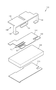
[42] FIG. 1 is a schematic exploded perspective view of a configuration of
an antenna
structure 100 according to an exemplary embodiment, and FIG. 2 is a side view
of the
antenna structure 100 illustrated in FIG. 1.
[43] Referring to FIGS. 1 and 2, the antenna structure 100 includes a
substrate 120, a
ground layer 110 that is formed on a bottom surface of the substrate 120, a
patch
antenna unit 140 which is formed on a top surface of the substrate 120 and to
which a
signal to be radiated is supplied, a shorting leg 154 that is shorted with the
patch
antenna unit 140, and a three-dimensional (3D) antenna unit 150 having a
radiation
unit for radiating a signal from the patch antenna unit 140.
144] The configuration of the antenna structure 100 according to the
current exemplary
embodiment may improve radiation efficiency while reducing the size of the
antenna
structure 100. When radiation of the antenna structure 100 occurs in a random
direction, the performance of the antenna structure 100 may deteriorate due to
a metal
structure that may be disposed adjacent to the antenna structure 100. For
example,
when the antenna structure 100 is disposed inside a camera, the antenna
structure 100
may be adjacent to a metal plate, such as a capacitor. In addition, since most
electronic
devices that have a wireless communication function include a structure that
is formed
of metal, such as a frame, a case, a panel, or the like, when the antenna
structure 100 is
disposed inside a device, the antenna structure 100 is adjacent to the metal
material,
and the radiation performance of the antenna structure 100 deteriorates.
However,
there is a difference in radiation efficiency of a chip antenna that is
designed in a 2.4
GHz band of 60% or more and 25%, respectively, when the antenna structure 100
is in
a wireless fidelity (WiFi) board state and when the antenna structure 100 is
installed on
the camera. In order to reduce the difference, the inventor suggests a
structure in which
radiation of the antenna structure 100 occurs less at a predetermined position
and the
predetermined position being adjacent to the metal material so that radiation
efficiency
of the antenna structure 100 that is disposed outside the device may be
improved.
[45] A more detailed configuration and operation of the antenna structure
100 will now be
described.
[46] Insulating substrates formed of various materials may be used as the
substrate 120.
The substrate 120 may be formed of a FR4 material, for example.
[47] The patch antenna unit 140 and the ground layer 110 that are formed on
the top and
bottom surfaces of the substrate 120, respectively, serve to make a resonant
mode
CA 02837561 2013-11-27
6
WO 2012/165797 PCT/ICR2012/004041
inside two metals and to combine with resonance that occurs due to the 3D
antenna
unit 150. In this regard, the ground layer 110 serves to reduce the effect of
any metal
that may be disposed adjacent to the antenna structure 100. Generally, when
the
antenna structure 100 is used, a printed circuit board (PCB) substrate
including a radio
frequency (RF) circuit for generating a signal to be radiated by the antenna
structure
100 may be provided, and the ground layer 110 may be shorted with a ground of
the
PCB substrate. In the current embodiment, such RF circuit may be embedded in
the
substrate 120, and a transmission line via which a signal generated by the RF
circuit is
transmitted to the patch antenna unit 140 may be embedded in the substrate 120
together with the RF circuit.
[48] The patch antenna unit 140 includes a feeding line FL to which a
signal to be
radiated is supplied. In addition, slit patterns for frequency tuning may be
formed on
the patch antenna unit 140. Although two slit patterns are formed in the patch
antenna
unit 140, as shown in exemplary embodiments of FIGS. 1 and 2, this is just an
example. One or more slit patterns may be formed in the patch antenna unit
140, or no
slit patterns may be formed in the patch antenna unit 140. In addition, the
shape of the
slit patterns is a groove shape that is recessed from a lateral portion of the
patch
antenna unit 140. However, other exemplary embodiments are not limited
thereto, and
the slit patterns may have an opening shape, for example. A detailed shape of
the patch
antenna unit 140 including the feeding line FL is not limited to the shape of
FIGS. 1
and 2 and may be modified in various ways according to the frequency of a
signal or a
feeding method, which will be described below.
[49] The 3D antenna unit 150 includes the shorting leg 154 that is shorted
with the patch
antenna unit 140 and the radiation unit that radiates a signal from the path
antenna unit
140. The 3D antenna unit 150 is used to make a resonance mode in a frequency
band
of a signal to be radiated together with the patch antenna unit 140. The 3D
antenna unit
150 serves to extend a length of the patch antenna unit 140. As the 3D antenna
unit 150
is introduced, the size of the patch antenna unit 140 may be reduced. For
example,
when a 2.4 GHz band design is used with only the patch antenna unit 140, the
size of
the patch antenna unit 140 is approximately 30X30 mm2. However, when the 3D
antenna unit 150 as well as the patch antenna unit 140 is used to design a 2.4
GHz
band device, the size of the patch antenna unit 140 is reduced to
approximately 7.5X4
mm2.
150] In more detail, the 3D antenna unit 150 includes a planar pattern unit
152 that is
spaced apart from the patch antenna unit 140 by a predetermined distance. The
shorting leg 154 and the radiation unit of the 3D antenna unit 150 extend from
the
planar pattern unit 152 towards the patch antenna unit 140.
[51] A detailed shape of the planar pattern unit 152 is properly designed
according to the
CA 02837561 2013-11-27
7
WO 2012/165797 PCT/ICR2012/004041
frequency of a signal to be radiated and is not limited to the shape shown in
the
exemplary embodiments of FIGS. 1 and 2. The slit patterns for frequency tuning
may
be formed in the planar pattern unit 152. Although one slit pattern is formed
in the
planar pattern unit 152, as illustrated in FIG. 2, this is just an example,
and a plurality
of slit patterns may be formed in the planar pattern unit 152, or no slit
patterns may be
formed on the planar pattern unit 152. In addition, the shape of the slit
pattern is a
groove shape that is recessed from a lateral portion of the planar pattern
unit 152.
However, other exemplary embodiments are not limited thereto, and slit
patterns
having an opening shape, for example, may be formed in the planar pattern unit
152.
11521 The shorting leg 154 includes a protrusion that protrudes from the 3D
antenna unit
150 by a length corresponding to a separation distance between the planar
pattern unit
152 and the patch antenna unit 140, and a bonding portion that is curved from
the
protrusion and extends in a direction parallel to a top surface of the patch
antenna unit
140. The bonding portion of the shorting leg 154 is shorted with the patch
antenna unit
140.
11531 The radiation unit may include at least one floating leg that extends
from one end of
the planar pattern unit 152 towards the patch antenna unit 140. At least one
floating leg
may be configured to support the planar pattern unit 152 together with the
shorting leg
154. The radiation unit may include a first floating leg 156 and a second
floating leg
158, as illustrated in FIG. 2. The first floating leg 156 and the second
floating leg 158
may be disposed at both sides of the shorting leg 154 therebetween. However,
the first
floating leg 156 and the second floating leg 158 are not limited to the
number, the
position, and the shape illustrated in FIG. 2.
11541 The first floating leg 156 and the second floating leg 158 may be
fixed on the
substrate 120 to support the planar pattern unit 152. To this end, ends of the
first
floating leg 156 and the second floating leg 158 may be bent in a direction
parallel to
the substrate 120. In addition, a first bonding pad 131 and a second bonding
pad 132
may be further formed on the substrate 120 so that the first floating leg 156
and the
second floating leg 158 are bonded to the substrate 120, respectively.
11551 FIGS. 3A through 3G illustrate examples of a feeding structure that
is employed in
the patch antenna unit 140 of the antenna structure 100 illustrated in FIG. 1.
11561 Line feeding, coupling feeding, or coaxial feeding may be used as a
feeding method
of the patch antenna unit 140.
157] FIGS. 3A, 3B, and 3C illustrate examples of line feeding whereby a
signal is directly
supplied to the antenna structure 100 of FIG. 1 via the feeding line FL. The
shape of
the patch antenna unit 140 may be modified in various ways, as well as the
rectangular
shape, the diamond shape, and the circular shape illustrated in FIGS. 3A, 3B,
and 3C,
respectively.
CA 02837561 2013-11-27
8
WO 2012/165797
PCT/ICR2012/004041
158] FIG. 3D
illustrates a coaxial feeding method, and FIGS. 3E, 3F, and 3G illustrate
examples of coupling feeding. As illustrated in FIG. 3E, the feeding line FL
may be
disposed on the same plane as the patch antenna unit 140, or as illustrated in
FIG. 3F,
the feeding line FL may be disposed on a different plane from that of the
patch antenna
unit 140, for example, inside the substrate 120. FIG. 3G illustrates an
example of slot
coupling in which a ground layer 110 having slots formed therein is formed on
a
bottom surface of the substrate 120 and the feeding line FL is formed below
the ground
layer 110' The feeding line FL may be formed inside a dielectric layer 120
that is
disposed under the ground layer 110' or may be formed on a surface of the
dielectric
layer 120'
[59] FIGS. 4 and 5 illustrate examples of slit patterns that may be
employed in the planar
pattern unit 152 or the patch antenna unit 140 of the antenna structure 100 of
FIG. 1 for
frequency tuning.
[60] Referring to FIG. 4, a slit pattern S has a groove shape that is
recessed from a lateral
portion of the planar pattern unit 152 or the patch antenna unit 140, and a
width w and
a length d of the slit pattern S having a groove shape may be adjusted for
proper
frequency tuning. The positions and number of slit patterns S are not limited
to the
exemplary embodiments of FIG. 4.
[61] Referring to FIG. 5, a slit pattern S may have an opening shape that
is formed
through the planar pattern unit 152 or the patch antenna unit 140. A width w
and a
length d of the slit pattern S having an opening shape may be adjusted for
proper
frequency tuning. However, the shape of the slit pattern S having an opening
shape is
not limited to the rectangular shape shown in the exemplary embodiment of FIG.
5.
[62] The slit patterns S illustrated in FIGS. 4 and 5 may be combined to
form in the planar
pattern unit 152 and the patch antenna unit 140.
[63] FIG. 6 illustrates a radiation path of a device employing the antenna
structure 100 of
FIG. 1 with a reduced effect of metal that is disposed adjacent to the antenna
structure
100 of FIG. 1. Radiation of the antenna structure 100 in a downward direction
is
reduced due to the ground layer 110 formed in a lower portion of the antenna
structure
100, and radiation of the antenna structure 100 in an upward direction is
relatively
increased. Thus, when the antenna structure 100 is disposed inside an
electronic device
that requires a wireless communication function, the ground layer 110 of the
antenna
structure 100 may be disposed adjacent to a metal structure formed inside the
electronic device, or may be attached to the metal structure so that radiation
efficiency
of the antenna structure 100 outside the electronic device may be improved.
Radiation
efficiency of the antenna structure 100 that is designed in a 2.4 GHz band is
ap-
proximately 60% when the antenna structure 100 is installed on a WiFi board,
and is
approximately 52% even when the antenna structure 100 is installed within a
camera.
CA 02837561 2013-11-27
9
WO 2012/165797 PCT/ICR2012/004041
Therefore, a reduction in efficiency due to the effect of metal disposed
adjacent to the
antenna structure 100 is very small.
[64] FIG. 7 is a schematic exploded perspective view of an antenna
structure 200
according to another exemplary embodiment.
[65] The antenna structure 200 according to the current exemplary
embodiment is
different from the antenna structure 100 of FIG. 1 in that a dielectric
carrier 220 is
further disposed between the patch antenna unit 140 and the planar pattern
unit 152 of
the 3D antenna unit 150.
[66] When the dielectric carrier 220 is disposed, the planar pattern unit
152 may be
formed on a top surface of the dielectric carrier 220, and the shorting leg
154 may
extend from the top surface of the dielectric carrier 220 to a bottom surface
of the di-
electric carrier 220 along a side surface of the dielectric carrier 220.
[67] In addition, a radiation unit of the 3D antenna unit 150 includes at
least one floating
leg that extends from one end of the planar pattern unit 152 in a direction of
the patch
antenna unit 140, and the at least one floating leg may extend from the top
surface of
the dielectric carrier 220 along the side surface of the dielectric carrier
220. Although
the first floating leg 156 and the second floating leg 158 are shown in FIG.
7, the
positions and number thereof are not limited to those shown in the exemplary
em-
bodiment of FIG. 7.
[68] The dielectric carrier 220 may be formed of a dielectric material
having a relative di-
electric constant that is greater than 1. Thus, the overall size of the
antenna structure
200 of FIG. 7 may be reduced as compared to that of the antenna structure 100
of FIG.
1 when the same frequency band is used for the respective designs. In
addition, since
the dielectric carrier 220 also serves to securely install the 3D antenna unit
150 on the
substrate 120, the first bonding pad 131 and the second bonding pad 132 that
securely
install the first floating leg 156 and the second floating leg 158 on the
substrate 120,
may not be required. In addition, ends of the first floating leg 156 and the
second
floating leg 158 do not have to be bent in a direction parallel to the
substrate 120.
[69] The shape of the dielectric carrier 220 is not limited to the shape
shown in the
exemplary embodiment of FIG. 7, and the shapes of the shorting leg 154 or the
first
floating leg 156 and the second floating leg 158 may be modified together
according to
the shape of the dielectric carrier 220.
[70] As described above, an antenna structure according to the one or more
embodiments
may have a small structure, and an effect on the antenna structure due to a
metal
material that is disposed adjacent to the antenna structure is reduced so that
radiation
efficiency of the antenna structure may be improved.
[71] Thus, when the antenna structure is employed in an electronic device
for wireless
communication, the antenna structure may be disposed inside the electronic
device in
CA 02837561 2013-11-27
10
WO 2012/165797 PC T/ICR2012/004041
which a metal material is disposed adjacent to the antenna structure, or the
antenna
structure may be attached to a metal structure so that there are minimal
limitations in a
space for installing the antenna structure.
[72] The foregoing exemplary embodiments are merely exemplary and are not
to be
construed as limiting the present inventive concept. The exemplary embodiments
can
be readily applied to other types of apparatuses. Also, the description of the
exemplary
embodiments is intended to be illustrative, and not to limit the scope of the
claims, and
many alternatives, modifications, and variations will be apparent to those
skilled in the
art.
CA 02837561 2013-11-27