Note: Descriptions are shown in the official language in which they were submitted.
CA 02837839 2013-11-29
WO 2012/168866
PCT/1B2012/052836
1
MANAGING OPERATOR MESSAGE BUFFERS IN A COUPLING FACILITY
BACKGROUND
One or more aspects of the present invention relate, in general, to processing
within a
computing environment, and in particular, to processing operator message
commands within
the computing environment.
Computing environments range from simple environments to more complex
environments.
A simple environment may include one processor executing one operating system,
while a
complex environment may include a plurality of processors or a plurality of
isolated memory
spaces executing various kinds of systems. For instance, a complex environment
may
include one or more logical partitions executing one or more operating systems
and at least
one logical partition executing coupling facility control code. Regardless of
whether the
computing environment is simple or complex, it is necessary to adequately test
the
components of the computing environment to ensure reliability and an
acceptable level of
performance.
One technique for testing components of a computing environment is by issuing
operator
commands at a console connected to the components, which are then processed by
the
intended components of the computing environment. Once the operator commands
are
processed, results are returned to the console for verification by the
operator of the console.
Operator commands may also be used for purposes other than testing. Again,
these operator
commands are issued by an operator at a console and processed by the intended
components
of a computing environment.
BRIEF SUMMARY
The shortcomings of the prior art are overcome and advantages are provided
through the
provision of a computer program product for managing buffers of a computing
environment.
The computer program product includes a computer readable storage medium
readable by a
CA 02837839 2013-11-29
WO 2012/168866
PCT/1B2012/052836
2
processing circuit and storing instructions for execution by the processing
circuit for
performing a method. The method includes, for instance, setting buffers of a
coupling
facility to either an active state or an idle state including responsive to a
start operator
message command having an associated operator message token value, setting the
operator
message token value in a selected buffer and making the selected buffer
active; and
determining that the selected buffer of a coupling facility of the computing
environment is to
be reset, the buffer including information relating to processing an operator
message
command sent remotely to the coupling facility from a processor image coupled
to, but
separate from, the coupling facility, the operator message command to perform
an action on
the coupling facility, the selected buffer including a token field having a
token value relating
the selected buffer to operator messages having operator message (OM) tokens
having the
same token value; and setting the determined buffer to an idle state in
response to the
determining indicating that the buffer is to be reset, wherein the buffer
includes a plurality of
fields including a timer to indicate a length of time an operator message has
been active for
the buffer, an operator message request length, and an operator message
response length.
Methods and systems relating to one or more aspects of the present invention
are also
described and claimed herein. Further, services relating to one or more
aspects of the
present invention are also described and may be claimed herein.
Additional features and advantages are realized through the techniques of one
or more
aspects of the present invention. Other embodiments and aspects of the
invention are
described in detail herein and are considered a part of the claimed invention.
BRIEF DESCRIPTION OF THE SEVERAL VIEWS OF THE DRAWINGS
One or more aspects of the present invention are particularly pointed out and
distinctly
claimed as examples in the claims at the conclusion of the specification. The
foregoing and
other objects, features, and advantages of one or more aspects of the
invention are apparent
from the following detailed description taken in conjunction with the
accompanying
drawings in which:
CA 02837839 2013-11-29
WO 2012/168866
PCT/1B2012/052836
3
FIG. 1 depicts one example of a computing environment to incorporate and use
one or more
aspects of the present invention;
FIG. 2A depicts one example of a processor of the computing environment of
FIG. 1
communicating with a coupling facility of the computing environment, in
accordance with
an aspect of the present invention;
FIG. 2B depicts one embodiment of details relating to a Send Message
instruction used in
accordance with an aspect of the present invention;
FIG. 3A depicts one example of a multiplexor used to control processing of
operator
message commands received at the coupling facility, in accordance with an
aspect of the
present invention;
FIG. 3B depicts one example of the logic used by the multiplexor of FIG. 3A to
control
processing of operator message commands, in accordance with an aspect of the
present
invention;
FIG. 4A depicts one example of buffers used in processing operator message
commands, in
accordance with an aspect of the present invention;
FIG. 4B depicts one example of further details of a buffer of FIG. 4A, in
accordance with an
aspect of the present invention;
FIG. 5 depicts examples of various possible states of a buffer, in accordance
with an aspect
of the present invention;
FIG. 6 depicts one embodiment of various commands used in accordance with an
aspect of
the present invention;
CA 02837839 2013-11-29
WO 2012/168866
PCT/1B2012/052836
4
FIG. 7A depicts one embodiment of details relating to using a Send Message
instruction to
issue a Start Operator Message command, in accordance with an aspect of the
present
invention;
FIG. 7B depicts one embodiment of the logic of a Start Operator Message
command used in
accordance with an aspect of the present invention;
FIG. 8A depicts one embodiment of details relating to using a Send Message
instruction to
issue a Read Operator Message command, in accordance with an aspect of the
present
invention;
FIG. 8B depicts one embodiment of the logic of a Read Operator Message command
used in
accordance with an aspect of the present invention;
FIG. 9A depicts one embodiment of details relating to using a Send Message
command to
issue a Delete Operator Message command, in accordance with an aspect of the
present
invention;
FIG. 9B depicts one embodiment of the logic of a Delete Operator Message
instruction used
in accordance with an aspect of the present invention;
FIG. 10 depicts one embodiment of a computer program product incorporating one
or more
aspects of the present invention;
FIG. 11 depicts one embodiment of a host computer system to incorporate and
use one or
more aspects of the present invention;
FIG. 12 depicts a further example of a computer system to incorporate and use
one or more
aspects of the present invention;
FIG. 13 depicts another example of a computer system comprising a computer
network to
incorporate and use one or more aspects of the present invention;
CA 02837839 2013-11-29
WO 2012/168866
PCT/1B2012/052836
FIG. 14 depicts one embodiment of various elements of a computer system to
incorporate
and use one or more aspects of the present invention;
FIG. 15A depicts one embodiment of the execution unit of the computer system
of FIG. 14
5 to incorporate and use one or more aspects of the present invention;
FIG. 15B depicts one embodiment of the branch unit of the computer system of
FIG. 14 to
incorporate and use one or more aspects of the present invention;
FIG. 15C depicts one embodiment of the load/store unit of the computer system
of FIG. 14
to incorporate and use one or more aspects of the present invention; and
FIG. 16 depicts one embodiment of an emulated host computer system to
incorporate and
use one or more aspects of the present invention.
DETAILED DESCRIPTION
In accordance with one or more aspects of the present invention, a capability
is provided to
facilitate processing of operator message commands received from one or more
sources. In
one example, the operator message commands are received by a coupling facility
from the
one or more sources, and the coupling facility processes the commands and
returns
responses to the source(s). In one particular example, at least one of the
sources is a
processor image coupled to, but separate from, the coupling facility. As
examples:
= The
processor image is a logical partition having central processor resources
associated therewith and capable of executing an operating system, and the
coupling facility
is within another logical partition having central processor resources
associated therewith
and capable of executing coupling facility control code, in which both logical
partitions are
within the same central processing complex (i.e., the same machine);
= The
processor image is a logical partition having central processor resources
associated therewith and capable of executing an operating system, and the
coupling facility
is within another logical partition having central processor resources
associated therewith
CA 02837839 2013-11-29
WO 2012/168866
PCT/1B2012/052836
6
and capable of executing coupling facility control code, in which both logical
partitions are
within different central processing complexes (i.e., the different machines);
and
= The processor image is a stand-alone machine (not virtualized in a
logical
partition) separate from a machine or logical partition capable of executing
the coupling
facility.
Each processor image includes one or more processors.
Examples of coupling facility operator commands include:
Configure ¨ take CHPID (Channel Path) on or off line; CP ¨ take CP (Central
Processor) on
or off line; Display ¨ show resources; Help <command> - command specific help;
Locate ¨
display SID (subchannel id) vector or SID frames; Mode ¨ set volatility mode;
PRY ¨ turn
PRY (machine level debug tool) on or off; Retrieve ¨ retrieve coupling
facility (CF)
information; Rideout ¨ set power failure rideout time; RType ¨ set response
type; Shutdown
¨ terminate CF operation; SMI ¨ turn System Monitor Instrument on or off;
Timezone ¨ set
timezone offset; Trace ¨ set trace control; Patch ¨ apply concurrent patch;
Dyndisp ¨ turn
dynamic coupling facility dispatching on or off; MTO ¨ turn MTO (message time
out) for
commands table on; VMDUMP ¨ force a coupling facility hardlong on VM; CFDUMP ¨
force non-disruptive dump; and NDDUMP ¨ nddump command. These commands are
described in "Processor Resource/Systems Manager Planning Guide", IBM
Publication No.
SB10-7036-04, Fifth Edition, January 2005.
In one particular example, the commands are testing the coupling facility in
that the
commands specify an action to be taken on the coupling facility, the action is
performed,
results are sent back to the initiator of the command (e.g., operating system
console,
coupling facility console, test program) and those results are analyzed either
manually by an
operator, analyst, etc. or programmatically. By enabling operator message
commands that
take action on the coupling facility to be initiated and/or sent from remote
sources other than
a coupling facility console, testing that can be performed on the coupling
facility is
enhanced, as well as operations that can be performed. This may result in
increased
reliability and/or performance of the coupling facility.
CA 02837839 2013-11-29
WO 2012/168866
PCT/1B2012/052836
7
One embodiment of a computing environment to incorporate and/or use one or
more aspects
of the present invention is described with reference to FIG. 1. In one
example, a computing
environment 100 includes a central processor complex (CPC) 102, which is based
on the
z/Architecture0 offered by International Business Machines Corporation (IBM ).
Aspects
of the z/Architecture0 are described in an IBM publication entitled
"z/Architecture
Principles of Operation," IBM Publication No. SA22-7832-08, August 2010. One
system
that may include central processor complex 102 is the zEnterprise 196 (z196)
system offered
by International Business Machines Corporation. IBM and z/Architecture0 are
registered
trademarks, and zEnterprise 196 and z196 are trademarks of International
Business
Machines Corporation, Armonk, New York, USA. Other names used herein may be
registered trademarks, trademarks or product names of International Business
Machines
Corporation or other companies.
Central processor complex 102 includes, for instance, one or more partitions
(processor
images) 104, a hypervisor partition106, one or more central processors 108,
and one or more
components of an input/output subsystem 110. Partitions may be physical
partitions or
logical partitions 104 (e.g., LPARS), and each partition includes a set of the
system's
hardware resources (physical or virtualized) as a separate system capable of
running
operating system software.
Each logical partition 104 is capable of functioning as a separate system.
That is, each
logical partition can be independently reset, initially loaded with an
operating system or
other control code, if desired, and operate with different programs. An
operating system or
application program running in a logical partition appears to have access to a
full and
complete system, but in reality, only a portion of it is available. A
combination of hardware
and licensed internal code (LIC), referred to as firmware, keeps a program in
one logical
partition from interfering with a program in a different logical partition.
This allows several
different logical partitions to operate on a single or multiple physical
processors in a time-
slice manner. (As used herein, firmware includes, e.g., the microcode,
millicode and/or
macrocode of the processor. It includes, for instance, the hardware-level
instructions and/or
data structures used in implementation of higher level machine code. In one
embodiment, it
includes, for instance, proprietary code that is typically delivered as
microcode that includes
CA 02837839 2013-11-29
WO 2012/168866
PCT/1B2012/052836
8
trusted software or microcode specific to the underlying hardware and controls
operating
system access to the system hardware.)
In this example, several of the logical partitions have a resident operating
system (OS) 120,
which may differ for one or more logical partitions. In one embodiment, at
least one logical
partition is executing the z/OSO operating system, offered by International
Business
Machines Corporation, Armonk, New York. Further, at least one logical
partition is
executing coupling facility control code (CFCC) 122, also offered by IBM , and
therefore,
is referred to as a coupling facility.
A coupling facility is, for instance, a non-volatile shared storage device
(e.g., hardware) that
includes multiple storage structures, such as cache, list and/or lock
structures, which are used
to provide unique functions for the computing environment. It is a shareable
facility having
storage and processing capabilities. For instance, a coupling facility is a
processor with
memory and special channels (CF Links) that executes coupling facility control
code
(CFCC), rather than a standard operating system. Information in the coupling
facility resides
in memory as CFCC, and the coupling facility does not have I/O devices, other
than the CF
links. An implementation of a coupling facility (a.k.a., Structured External
Storage) is
described in U.S. Patent No. 5,317,739, entitled "Method and Apparatus for
Coupling Data
Processing System," Elko et al., issued May 31, 1994.
Logical partitions 104 are managed by hypervisor 106, which is implemented by
firmware
running on central processors 108. Logical partitions 104 and hypervisor 106
each
comprises one or more programs residing in respective portions of main memory
associated
with the central processors. One example of hypervisor 106 is the Processor
Resource/Systems Manager (PR/SMTm), offered by International Business Machines
Corporation, Armonk, New York.
Central processors 108 are physical processor resources that are allocated to
the logical
partitions. For instance, a logical partition 104 includes one or more logical
processors, each
of which represents all or a share of a physical processor resource 108
allocated to the
partition. The logical processors of a particular partition 104 may be either
dedicated to the
CA 02837839 2013-11-29
WO 2012/168866
PCT/1B2012/052836
9
partition, so that the underlying processor resource is reserved for that
partition; or shared
with another partition, so that the underlying processor resource is
potentially available to
another partition.
Input/output subsystem 110 (of which only a portion is depicted) provides
connectivity to
I/O devices. In one particular example of the z/Architecture0, the I/O
subsystem includes a
channel subsystem, which directs the flow of information between I/O devices
and main
storage. However, the I/O subsystem may be other than a channel subsystem.
The channel subsystem uses one or more channel paths as the communication link
in
managing the flow of information to or from the I/O devices. Within the
channel subsystem
are subchannels.
One subchannel is provided for and dedicated to each I/O device accessible to
the channel
subsystem. Each subchannel contains storage for information concerning the
associated I/O
device and its attachment to the channel subsystem. The subchannel also
provides storage
for information concerning I/O operations and other functions involving the
associated I/O
device. Information contained in the subchannel could be accessed by CPUs
using I/O
instructions as well as by the channel subsystem and serves as the means of
communication
between any CPU and the channel subsystem concerning the associated I/O
device.
Although a logically partitioned environment is described herein as one
computing
environment to incorporate and use one or more aspects of the present
invention, other
environments may also incorporate and/or use one or more aspects of the
present invention.
For instance, an environment having one or more processors coupled to a
coupling facility
(not a logically partitioned environment) may also incorporate and use one or
more aspects
of the present invention. Other examples are also possible.
Communication between a processor and a coupling facility, whether or not in a
logically
partitioned environment, is facilitated by one or more intersystem channels,
as depicted in
FIG. 2A. In the example described herein, the communication is between logical
partitions.
For instance, a logical partition 200 executing an operating system 204, such
as the z/OSO
CA 02837839 2013-11-29
WO 2012/168866
PCT/1B2012/052836
operating system, communicates with a logical partition 206 executing coupling
facility
control code 208 via at least one intersystem channel 210. In particular, in
one example,
logical partition 200 communicates with logical partition 206 over the
intersystem channel(s)
via a Send Message (SMSG) protocol 220.
5
In one example, the Send Message protocol includes a Send Message instruction
which
initiates a message operation. The message operation is controlled by
information in the
Send Message instruction, as well as a message operation block indicated in
the Send
Message instruction. The message operation includes executing a command
specified in a
10 message command block (e.g., for one or more aspects of the present
invention, a Start
Operator Message command, a Read Operator Message command and/or a Delete
Operator
Message command, described below). Further, during performance of the
operation,
response information is stored in a message response block in main storage.
Further details regarding the Send Message protocol are described with
reference to FIG. 2B.
A send message instruction 250 has two operands, including a message
operations block
(MOB) 252 and a designation of a subchannel 254 located in a channel subsystem
256. The
message operations block includes, for instance, a message command block
address 258
pointing to a message command block 264/message response block 266 pair. These
are 256-
byte buffers located in main memory. Message operations block 252 also
includes a
message buffer address list (MBAL) address 260 that points to a message buffer
address list
268. The MBAL list is a variable length list from, for instance, 1-16. It
includes one or
more message buffer address words (MBAWs) 268 that designate one or more
message
buffers 272. The buffers may be a source for write operations to coupling
facility 206 or a
target of read operations from the coupling facility. Also included in message
operation
block 252 is a MBAL length 262 that indicates the length of the MBAL list. Not
all
commands have to have a message buffer address list, and therefore, the length
could be
zero. Message command block 264 includes the parameters that are sent to the
coupling
facility, and when a response comes back it is stored directly to the MRB.
When Send Message is executed, parameters from the message operation block are
passed to
the CPU or channel subsystem requesting that a send function be performed with
the
CA 02837839 2013-11-29
WO 2012/168866
PCT/1B2012/052836
11
coupling facility associated with a specified subchannel of the channel
subsystem. The send
function is performed synchronously or asynchronously to Send Message.
The send function is performed by using information in the subchannel to find
a path to the
coupling facility. Using the path, the message operation is forwarded to the
coupling
facility. For instance, execution of the message operation is accomplished by
passing
command information to the coupling facility, decoding and executing the
command,
formulating response information indicating the result, and storing the
response information
in the message response block.
Status indications summarizing conditions detected during the execution of the
send function
are placed at the subchannel and made available to the operating system.
Additional details
regarding Send Message are described in U.S. Patent No. 5,561,809, entitled
"In A
Multiprocessing System Having A Coupling Facility, Communicating Messages
Between
The Processors And The Coupling Facility In Either A Synchronous Operation Or
An
Asynchronous Operation," Elko et al., issued October 1, 1996.
Continuing with FIG. 2A, in this example, coupled to logical partition 200 are
one or more
operating system consoles 230, as well as one or more test programs 232, which
may be
running within the same logical partition, the same central processing complex
but a
different logical partition, or another system. Similarly, coupled to logical
partition 206 is at
least one coupling facility console 234. Each console enables a user to enter
operator
message commands to its respective logical partition. Further, test program
232 is also able
to issue operator message commands to its respective logical partition.
Operator message
commands issued to logical partition 206 (also referred to herein as the
coupling facility)
from console 234 are received, in one example, by an operator message
processor 240 within
the coupling facility that services the commands received from the coupling
facility console.
Prior to one or more aspects of the present invention, the only remote entity
that could send
coupling facility operator message commands directly to the coupling facility
and receive
responses back was the coupling facility console. The testing of coupling
facility operator
commands required a person to log onto the coupling facility console to issue
the commands
CA 02837839 2013-11-29
WO 2012/168866
PCT/1B2012/052836
12
and verify the results. Other remote entities, such as operating systems,
operating system
consoles, test programs, and/or other remote systems, could not directly
access the coupling
facility to have operator message commands processed and the results returned.
Instead, any
such commands had to be forwarded to the coupling facility console, and since
some
commands could not be forwarded, those commands could not be processed by the
coupling
facility. Any results of commands processed by the coupling facility would be
returned to
the coupling facility console and displayed on the console.
In accordance with one or more aspects of the present invention, operator
message
commands are received at the coupling facility from console 234, as well as
logical partition
200 (and/or other logical partitions, processors, systems, etc.). For
instance, operator
message commands are received at logical partition 200 from consoles 230
and/or test
programs 232 (as well as other possible initiators), and then forwarded from
logical partition
200 to logical partition 206. To forward an operator message command from
logical
partition 200 to logical partition 206, in one example, an operator message
(OM) request 222
is sent from logical partition 200 to logical partition 206 using the Send
Message protocol
over the intersystem channel(s). The request includes, for instance, a command
that
specifies the requested operator message command. The coupling facility
processes the
request and using SMSG sends an operator message (OM) response 224 back from
logical
partition 206 to logical partition 200.
Since the coupling facility is now able to receive operator message commands
from
multiple, distinct sources, including, for instance, a coupling facility
console and one or
more logical partitions (or other processors, systems, etc.) coupled thereto,
controls are
provided within the coupling facility to manage the multiple requests to be
processed. One
such control is a multiplexor, an example of which is depicted in FIG. 3A.
As shown in FIG. 3A, a multiplexor 300 receives operator message commands from
multiple
sources 302, including a logical partition executing an operating system and
the coupling
facility console, as examples. In particular, in one example, the multiplexor
receives
operator message commands directly from the coupling facility console, and
directly from
the logical partition via a Start Operator Message command sent using SMSG.
The
CA 02837839 2013-11-29
WO 2012/168866
PCT/1B2012/052836
13
multiplexor is located within the coupling facility and is coupled to operator
message
processor 240. Thus, the operator message commands issued from the coupling
facility
console are now forwarded to the multiplexor, which directs the forwarding of
those
commands to the operator message processor. Similarly, operator message
commands
received from the logical partition (or other remote entities) are also input
to multiplexor
300. Further, other commands issued by the logical partition that are
associated with the
processing of the operator message commands (e.g., Read Operator Message and
Delete
Operator Message) are also input to multiplexor 300. Thus, for convenience,
the commands
that include the operator message commands, as well as other operations
associated
therewith, are referred to herein as SMSG commands. The multiplexor directs
the received
commands (i.e., the operator message commands from the coupling facility
console and the
SMSG commands) to the operator message processor.
One embodiment of the logic used by the multiplexor to control selection of
commands to be
processed by the operator message processor is described with reference to
FIG. 3B.
Initially, the multiplexor is idle, waiting for commands to be received, STEP
350. If there
are no commands, INQUIRY 352, then the multiplexor remains idle, STEP 350.
Otherwise,
if at least one command is received, one of the commands is sent to the
operator message
processor for processing, STEP 354. For example, the first command that is
received is sent
or if both operator message commands and SMSG commands are received, in this
example,
one of the SMSG commands is sent.
The operator message processor processes the command, as described further
below, and
outputs the results, STEP 356. If the command is from the coupling facility
console, the
results are output to the console. However, if the command is from a
processor, then the
results are stored in a buffer, as described below, and provided to the
coupling facility
console, in this example.
Thereafter, a determination is made as to whether there are any pending
commands from
sources other than the coupling facility console (e.g., pending SMSG
commands), INQUIRY
358. If there is at least one pending SMSG command, processing continues with
STEP 354
in which a command is selected and sent to the operator message processor.
Otherwise, a
CA 02837839 2013-11-29
WO 2012/168866
PCT/1B2012/052836
14
check is made to see if there are any pending commands from the coupling
facility console,
INQUIRY 360. If there is one or more pending console commands, then processing
continues with STEP 354. However, if there are no more pending console
commands, then
processing continues to STEP 350.
Multiple commands may be received from one or more logical partitions coupled
to the
coupling facility (i.e., from non-CF logical partitions, which are partitions
that do not include
coupling facility control code). Thus, the coupling facility includes one or
more buffers
(referred to herein as operator message (OM) processing buffers) to store the
incoming
commands from such partitions. Further details regarding the buffers are
described with
reference to FIGs. 4A-4B.
Referring to FIG. 4A, in one example, the coupling facility includes one or
more buffers
400. In this example, there are nine buffers, but this number of buffers is
configurable.
Each buffer 400 has a plurality of controls associated therewith, as described
with reference
to FIG. 4B.
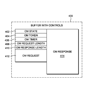
With reference to FIG. 4B, buffer 400 includes, for instance:
Operator message state 402, which indicates the state of the buffer including
idle; active and
in process; or active, response pending, as described below.
Operator message token (OMTK) 404, which is a value provided by the operating
system
(e.g., the operating system console, which includes operating system code, or
the portion of
the operating system running in the logical partition) when the operator
message process is
started. The operator message token uniquely identifies the operator message
request. When
the operator message processing buffer is idle, the operator message token
contains zeros.
This token is used to identify a buffer, once it is selected.
Operator message timer (OMT) 406, which is a time-of-day value that is set
when the
operator message request is started. It is set to the current value of the
time-of-day clock.
The operator message timer is used to determine the length of time that the
operator message
CA 02837839 2013-11-29
WO 2012/168866
PCT/1B2012/052836
has been active. When the operator message processing buffer is idle, the
operator message
timer contains zeros.
Operator message request length (OMREQL) 408, which is a value that contains
the length,
5 in bytes, of the OM request (e.g., the operator message command). When
the OM
processing buffer is idle, the value of the OMREQL object is zero.
Operator message response length (OMRESL) 410, which is a value that contains
the length,
in bytes, of the OM response. When the OM processing buffer is idle or when
the OM
10 processing buffer is active and processing, the value of the OMRESL
object is zero.
Operator message request data (OMREQD) 412, which includes the contents of the
OM
request passed into the coupling facility by the Start Operator Message
command (described
below). When the OM processing buffer is idle, the contents of the OM request
data are
15 undefined.
Operator message response data (OMRESD) 414, which includes the results of the
operator
message command. When the operator message processing buffer is idle, or when
the
operator message processing buffer is active and processing, the contents of
the OM
response data are undefined.
As described above, each buffer has various states associated with it.
Referring to FIG. 5,
initially, a buffer is in the idle state 500. This indicates that it is
available for starting a
message. Responsive to a Start Operator Message command, the buffer
transitions into an
active and in process state 502, which indicates that the operator message
command is being
processed by the coupling facility. In particular, operator message processor
240 processes
the request, including the operator message command, in the background and
provides a
response. Responsive to generating the response, the buffer is placed in an
active, response
pending state 504. At this point, a read operation that is querying the
buffers can access the
buffer and read out the response.
CA 02837839 2013-11-29
WO 2012/168866
PCT/1B2012/052836
16
Thereafter, the buffer may be returned to the idle state via for instance, a
timeout that the
coupling facility (i.e., the operator message processor) recognizes, or
explicitly by a Delete
Operator Message or Start Operator Message. Further details regarding the
buffers and
processing thereof are described below.
An operator message (OM) processing buffer is an area of coupling facility
storage that
contains information related to the processing of an operator message command
sent via the
Start Operator Message (SOM) command. The OM processing buffer is assigned
from an
area of coupling facility storage that is not available for structure
allocation.
The OM processing buffer is either active or idle. When idle, it is available
for selection by
the Start Operator Message (SOM) command. When active, an operator message
process
has been started and has not yet been deleted. If the operator message
response is available,
the buffer state is active with response pending. Otherwise, the buffer state
is active and
processing.
Deleting an active operator message process with response pending resets the
objects
associated with the OM processing buffer and places the buffer in the idle
state (a.k.a.,
resetting an OM processing buffer).
There are three ways an active operator message process can be deleted:
1. A Delete Operator Message command is executed that specifies an OM token
that matches the OM token object and the OM processing buffer is active with
response
pending.
2. The length of time that the operator message process has been active
exceeds the
value of the OM timeout control and the OM processing buffer is active with
response
pending. This may be detected by an internal coupling facility process or by a
Start Operator
Message command.
CA 02837839 2013-11-29
WO 2012/168866
PCT/1B2012/052836
17
3. A Start Operator Message command is executed that specifies
an OM token that
matches the OM token object and the OM processing buffer is active with
response pending,
and all message buffers are busy and at least one has timed out.
A lag in time may occur between the time the OM processing buffer times out
and when it is
detected as timed out and reset to the idle state. In this case, the OM
processing buffer
remains active with response pending until the OM request is deleted.
Processing an OM request is performed as a background operation. The
background process
is initiated when a Start Operator Message command successfully completes. The
background process generates the OM response data, stores the response data in
the
OMRESD object and stores the response length in the OMRESL object. It then
changes the
state of the OM processing buffer to active with response pending.
Further details regarding buffer processing, and in particular, the Operator
Message
commands are described below. However, prior to that description other objects
and
operands are described to facilitate understanding of one or more aspects of
the present
invention.
As an example, the coupling facility includes a number of global objects used
to process the
operator message commands. These objects include, for instance:
A fixed global control ¨ e.g., an operator message processing buffer count
(OMPBC), which
is a model-dependent value that specifies the number of OM processing buffers
supported by
the coupling facility;
Program modifiable global controls ¨ e.g., operator message processing buffers
(OMPB),
and an operator message timeout control (OMTOC), which is a value that
determines the
maximum length of time, in seconds, that an operator message is associated
with an OM
processing buffer. If an operator message has not been explicitly deleted
before the timeout
value is exceeded, the operator message is deleted by the coupling facility
and the OM
processing buffer is placed in the idle state. In one example, the default
value is 300; and
CA 02837839 2013-11-29
WO 2012/168866
PCT/1B2012/052836
18
Facility attributes (FACA) ¨ e.g., an operator message facility indicator,
which is a value
that specifies whether or not the facility described herein for processing
operator message
commands is supported by the coupling facility.
Further, the coupling facility includes a plurality of global operands used in
processing
operator message commands. In one example, these operands include:
Operator Message (OM) Request (OMREQ): A variable length byte string with a
maximum
length of a pre-specified number of bytes (e.g., 192 bytes) that includes the
operator message
command to be processed. The length is specified by the OM request length.
Operator Message (OM) Response (OMRES): A variable length byte string with a
maximum length of a pre-defined number of bytes (e.g., 4096 bytes). The length
is specified
by the OM response length.
Operator Message (OM) Timeout Control (OMTOC): A value that determines the
maximum length of time, in seconds, that an operator message is associated
with an OM
processing buffer. As an example, valid values range from 5 to 300. This
operand is
ignored unless the update OMTOC indicator is valid and is set to a value that
indicates the
OM timeout control is to be updated.
Operator Message (OM) Token (OMTK): A value that uniquely identifies an
operator
message process.
Update OMTOC Indicator (UOMTCI): A value that indicates whether the operator
message
timeout control should be updated. It has the following encoding, as examples:
do not
update the OM timeout control; update the OM timeout control.
In accordance with one or more aspects the present invention, operator message
commands
can be sent to the coupling facility from coupling facility consoles, as well
as logical
partitions or other systems, processors, etc., coupled to the coupling
facility. Processing
CA 02837839 2013-11-29
WO 2012/168866
PCT/1B2012/052836
19
associated with sending operator message commands to the coupling facility
from sources
other than coupling facility consoles is described with reference to FIG. 6.
Initially, a command is entered or generated by an initiator, such as an
operating system
console or a test program, as examples, STEP 600. Responsive thereto, the
operating system
(e.g., the portion executing on the console or executing the test program)
generates an
operator message token, STEP 602. In one example, the token is generated by
concatenating
a system identifier with a time-of-day clock value. Thereafter, the initiator
issues a Start
Operator Message (SOM) request, which includes the token, as well as the
requested
operator message command, STEP 604. The Start Operator Message request is sent
to the
logical partition coupled to the initiator.
At the logical partition, the operating system creates the Start Operator
Message command
by placing the start request, including the token and requested operator
message command,
in a message command block of the Start Operator Message command. The message
command block is then sent from the operating system to the coupling facility
via a SMSG
command. The multiplexor receives the SMSG command and forwards it to the
operator
message processor, in due course. The operator message processor then
processes the
command, as described below. As part of processing, a response is generated.
The response to the Start Operator Message command is forwarded back to the
initiator of
the SOM. For instance, the response is included in a message response block
forwarded to
the logical partition via SMSG. Then, from the logical partition, the response
is forwarded
to the initiator.
The initiator (e.g., operating system console, test program) receives the
response and checks
the value of the response code, INQUIRY 606. If the response code indicates
that all the
buffers are already active, and therefore, not available, processing returns
to STEP 604.
However, if the response code indicates that the operator message has been
started,
processing continues with STEP 610. Otherwise, an error message is issued,
STEP 608.
CA 02837839 2013-11-29
WO 2012/168866
PCT/1B2012/052836
At STEP 610, a Read Operator Message command is issued by the initiator to
read the buffer
to obtain the response provided by the coupling facility responsive to
processing the operator
message command in the Start Operator Message. For instance, a Read Operator
Message
request issued by the initiator is received at the logical partition (e.g.,
operating system),
5 which creates the Read Operator Message command and forwards it from the
operating
system to the coupling facility via SMSG. The coupling facility, and in
particular, the
multiplexor receives the SMSG command and forwards it, in turn, to the
operator message
processor. The operator message processor processes the read command, as
described
below, and sends a response code. The response code is ultimately returned to
the initiator,
10 as described above. The response code is checked, INQUIRY 612, and if
the response
indicates that an OM response is not available, then processing returns to
STEP 610.
However, if the response code indicates that an OM response is available, then
the buffer is
read to obtain the results of the requested operator message command.
Processing then
continues with STEP 616, in one embodiment. Otherwise, an error message is
issued, STEP
15 614.
At STEP 616, a delete operator message request is issued by the initiator and
received at the
logical partition. The operating system generates a Delete Operator Message
command and
sends it to the coupling facility via SMSG, as described above. The Delete
Operator
20 Message command is processed by the operator message processor, as
described below, and
a response is returned to the initiator. The initiator checks the response
code to the Delete
Operator Message command, INQUIRY 618. If the response code indicates that the
operator message was deleted, then the OM response is provided to the issuer,
STEP 620.
Otherwise, an error message is issued, STEP 622.
As indicated above, there are various message commands that are used in
accordance with
one or more aspects of the present invention. One such command is the Start
Operator
Message command, an embodiment of which is described with reference to FIG. 7A-
7B.
In one example, an operator message command is initiated through, for
instance, the z/OSO
console or a test program. It flows into the z/OSO logical partition and is
sent across to the
CA 02837839 2013-11-29
WO 2012/168866
PCT/1B2012/052836
21
coupling facility through Send Message in a Start Operator Message command.
One
embodiment of this processing is described with reference to FIG. 7A.
As described above, the Send Message instruction 250 includes a message
operations block
252 and a designation of a subchannel 254. In this case, however, for a Start
Operator
Message command, the message operations block only includes a message command
block
address 258, which points to MCB 264/MRB 266. For this operation, there are no
message
blocks. The message command block presented to the coupling facility includes
a Start
Operator Message MCB 780 having, for instance, Start Operator Message request
parameters 782 and an operator message request 784 that specifies the
requested operator
command. The response that comes back is a Start Operator Message MRB 790
including
Start Operator Message response parameters 792, which include a response code.
In one example, Start Operator Message request parameters include a token, the
request, and
a request length. The coupling facility and, in particular, the operator
message processor via
the multiplexor, receives the SMSG command block and begins processing the
Start
Operator Message command, as described with reference to FIG.7B.
Initially, the operator message processor scans the operating message buffers
looking for an
idle buffer (e.g., OMTK has zeros), STEP 700. A determination is made as to
whether there
are any idle buffers, INQUIRY 702. If there is an idle buffer, then an idle
buffer (e.g., the
first) is selected, STEP 704. Thereafter, the operator message token is stored
in the buffer,
STEP 706. Further, an operator message timer in the buffer is set to the
current time, STEP
708. In one example, the time is obtained from a time-of-day clock. Further,
the request and
request length are stored in the buffer, STEP 710, and the buffer state is set
to active and in
process (a.k.a., active and processing), STEP 712. A return code is returned
to the operating
system (e.g., z/OSO) indicating the buffer is set, STEP 714, and eventually to
the initiator.
This processing is performed synchronously to the z/OSO program.
Returning to INQUIRY 702, if there are no idle buffers, then the operator
message buffers
are scanned once again looking for active buffers that have timed out, STEP
720. A
determination is made as to whether there are any active buffers that have
timed out,
CA 02837839 2013-11-29
WO 2012/168866
PCT/1B2012/052836
22
INQUIRY 722. If not, then a return code is provided indicating that there are
no buffers
available, STEP 724.
However, if there are any active buffers that have timed out, then a timed out
buffer is
selected, STEP 726. In one example, it is the first timed out buffer that is
selected. The
buffer is set to the idle state, STEP 728, and processing continues with STEP
706, in which
the buffer is initialized.
Further details regarding the Start Operator Message command are described
below. As
indicated herein, this command, as well as the Read Operator Message command
and the
Delete Operator message command, are communicated to the coupling facility
using SMSG.
SMSG sends a message from the logical partition to the coupling facility that
includes the
requested command. To send the message, the message is included in a message
command
block (MCB) and any response to the message is included in a message response
block
(MRB).
In one example, the message command block for the Start Operator Message
includes: a
message header; the command (e.g., Start Operator Message); the OM request
length; the
operator message token; and the operator message request (e.g., the operator
message
command).
In operation, the value of the OM token provided in the request is compared to
the OM token
object in each OM processing buffer. If the OM token is valid and does not
match any OM
token object, and if at least one OM processing buffer is idle, an idle buffer
is selected. If no
OM processing buffers are in the idle state and at least one OM processing
buffer is active
with response pending and has exceeded the timeout value, a timed out buffer
is selected and
reset to the idle state.
Once an idle buffer is selected, the OM token is placed in the OMTK object,
the OM request
is placed in the OMREQD object, the OM request length is placed in the OMREQL
object,
the OM timer object is set to the value of the time-of-day clock, the buffer
is placed in the
active and processing state, and a background process is initiated to generate
the OM
CA 02837839 2013-11-29
WO 2012/168866
PCT/1B2012/052836
23
response (i.e., begin processing the requested operator message command and
place
information (e.g., results regarding the OM command) in the buffer). A return
code is
returned to the operating system indicating an operator message has started.
If the OM token matches an OM token object for an active OM processing buffer,
no
processing occurs. The command is completed and a response code is returned
indicating an
operator message has started.
If the OM token is valid, does not match any OM token object, and all buffers
are either
active and processing or active with response pending without exceeding the
timeout control,
the command is completed and a response code is returned indicating no
available buffers.
The response is returned in a message response block, which includes, for
instance, a
response descriptor and the response code.
Responsive to receiving a response indicating that the operator message has
been started, a
Read Operator Message command is issued to obtain the response to the
requested operator
message command. Referring to FIG. 8A, the Read Operator Message command is
sent via
the Send Message protocol. As described above, Send Message instruction 250
includes a
message operations block 252 and a designation of a subchannel 254. For a Read
Operator
Message command, message operations block 252 includes MCB address 258, MBAL
address 260, and MBAL length 262. For the Read Operator Message command, the
MBAL
length is equal to one and MBAL address 260 points to MBAL 268 having one
entry.
MBAL 268 points to a message buffer 272.
MCB address 258 designates an MCB 264/MRB 266 pair. The message control block
880
for the Read Operator Message command includes the Read Operator Message
request
parameters 882 (e.g., message header, read command, OM token), which are
forwarded to
the coupling facility for processing. Responsive to processing the Read
Operator Message
command, Read Operator Message response parameters (e.g., a response code) are
returned
in MRB 266. Additionally, an operator message (OM) response 875 is returned
and placed
in message buffer 272.
CA 02837839 2013-11-29
WO 2012/168866
PCT/1B2012/052836
24
One embodiment of the logic of the Read Operator Message Command is described
with
reference to FIG. 8B. Initially, the operator message buffers are scanned for
a buffer with an
OM token that matches the OM token provided in the command, STEP 800. If there
is no
buffer with a matching OM token, INQUIRY 802, then a response code is returned
indicating no matching token found, STEP 804.
However, if there is an OM buffer with a matching OM token, then a
determination is made
as to whether there is an OM response pending in the buffer, INQUIRY 806. If
there is not
an OM response pending, then a response code is returned indicating OM
response not
available, STEP 808.
Returning to INQUIRY 806, if there is an OM response pending, then the OM
response is
copied to a data block (e.g., located within message buffer 272) specified by
SMSG, STEP
810, and the response length is copied to the message response block, STEP
812. The OM
response (i.e., the data block) is returned, as well as a response code
indicating an OM
response is available, STEP 814.
Further details regarding the Read Operator Message command are described
below. In one
example, the message command block for the Read Operator Message command
includes a
message header; the read command; and the operator message token.
In operation, when sufficient message buffer space (e.g., buffer 272) is
provided (i.e., buffer
space equal to or greater than a pre-specified size is available), the value
of the OM token is
compared to the OM token object in each OM processing buffer.
If the OM token matches an OM token object for an OM processing buffer and the
buffer is
active with response pending, the OM response is placed in a data block. The
data block, the
OM request, the OM request length, the OM response length, and a response code
indicating
an OM response is available are returned. The response, except the data block,
is returned in
a message response block, which includes, for instance, a response descriptor,
the response
code, the OM request length, the OM response length, and the OM request. The
data block
is returned via SMSG but separate from the response block.
CA 02837839 2013-11-29
WO 2012/168866
PCT/1B2012/052836
If the OM token matches an OM token object for an OM processing buffer that is
active and
processing, no processing occurs. The command is completed and a response code
is
returned to the program indicating an OM response is not available. The
response is
returned in a response block, which includes, for instance, a response
indicator and the
5 response code.
If the OM token is valid but does not match any OM token object for an active
OM
processing buffer, no processing occurs. The command is completed and a
response code is
returned indicating no matching token found. The response is returned in a
response block,
10 which includes, for instance, a response indicator and the response
code.
When the message buffer size is less than a pre-specified size, there is
insufficient message
buffer space (e.g., buffer 272) to contain the data block. (In this case, no
processing occurs,
the command is competed and a response code is returned indicating
insufficient message
15 buffer space. The response is returned in a response block, which
includes, for instance, a
response indicator and the response code.
Subsequent to receiving the response, a decision may be made to reset the
buffer. Thus, a
Delete Operator Message command is issued. Referring to FIG. 9A, as with the
other
20 operator message commands, the Delete Operator Message command is sent
to the coupling
facility via the Send Message protocol. Again, Send Message instruction 250
includes a
message operation block 252 and a designation of subchannel 254. In this case,
the message
operation block includes MCB address 258 pointing to MCB 264/MRB 266 pair. The
MCB
980 for the Delete Operator Message includes delete operator message request
parameters
25 982 (e.g., message header, delete command, and OM token), which are
forwarded to the
coupling facility. Responsive to performing the Delete Operator Message
command, a
Delete Operator Message MRB 990, including Delete Operator Message response
parameters, are returned in MRB 266.
One embodiment of the logic of the Delete Operator Message Command performed
by the
operator message processor is described with reference to FIG. 9B. Initially,
the OM buffers
are scanned for a buffer with a matching OM token, STEP 900. If there is not a
buffer with
CA 02837839 2013-11-29
WO 2012/168866
PCT/1B2012/052836
26
a matching OM token, INQUIRY 902, a response code is returned indicating
operator
message deleted, STEP 904.
However, if there is a buffer with a matching OM token, INQUIRY 902, then a
further
determination is made as to whether an OM response is pending, INQUIRY 906. If
an OM
response is not pending, a response code is returned indicating the buffer is
active and
processing, STEP 908.
If there is an OM response pending, INQUIRY 906, the OM token, the OM timer,
the
request length and the response length are reset, e.g., set to zero, STEP 910.
Further, the
OM buffer state is set to idle, STEP 912, and a response code is returned
indicating operator
message deleted, STEP 914. (In a further embodiment, setting a buffer to an
idle state
deletes the buffer; and setting an idle buffer to an active state, creates a
new buffer.)
Further details regarding the Delete Operator Message command are described
below. In
one example, the message command block for the Delete Operator Message command
includes a message header; the Delete Operator Message command; and the
operator
message token.
In operation, the value of the OM token is compared to the OM token object in
each OM
processing buffer. If the OM token matches the value of an OM token object in
an active
OM processing buffer and the buffer is active with response pending, the
objects in the OM
processing buffer are reset and the buffer is placed in the idle state. When
the buffer objects
have been reset, the command is completed and a response code is returned to
the operating
system indicating the operator message is deleted.
When the OM processing buffer is active and processing, no action occurs. The
command is
completed and a response code is returned indicating the buffer is active and
processing.
When the OM token is valid but does not match the OM token object for any
active OM
processing buffer, no action occurs. The command is completed and a response
code is
returned to the program indicating the operator message is deleted.
CA 02837839 2013-11-29
WO 2012/168866
PCT/1B2012/052836
27
The response is returned in a message response block, which includes, for
instance, a
response descriptor and the response code.
Described in detail above are various commands to process operator message
requests.
These commands are part of an Operator Message facility, in this example. The
Operator
Message facility includes other commands, which are described herein for
completeness.
These commands include a Read Facility Parameters command and Set Facility
Authority
command.
For the Read Facility Parameters command, the message request block includes,
for
instance, a message header and the Read Facility Parameters command. In
operation, the
values of coupling facility controls are placed in the response operands, and
a response code
indicating success, if true, is stored in the response code operand. This
command may place
a number of controls in the response operands, however, for the Operator
Message Facility,
the operator message processor buffer count is placed in the OMPBC, and the
operator
message timeout control is placed in the OMTOC.
When the response code indicates that the coupling facility control values are
returned, the
message response block that is returned includes, for instance, a response
descriptor, the
response code, OM processor buffer count, and OM timeout control for the
Operator
Message Facility. Other controls may also be returned for other facilities.
For the Set Facility Authority command, the message request block includes,
for instance, a
message header, the Set Facility Authority command, an OM timeout control, an
update
OMTOC indicator, a comparative authority control and an authority control,
described
below.
In operation, a coupling facility authority control value is compared to a
comparative
authority (CAU) operand received in the message command block. When they
compare as
equal, the value of an authority (AU) operand received in the message command
block is
stored in the coupling facility authority control and the coupling facility
state is updated.
CA 02837839 2013-11-29
WO 2012/168866
PCT/1B2012/052836
28
When the coupling facility authority control is changed from zero to a nonzero
value, the
coupling facility state is changed from non-managed to managed, the OM timeout
control is
conditionally updated, an activate-message-path command is issued on each
message path to
a remote coupling facility, and a response code indicating success is
returned. If the update-
Om-timeout indicator is one, the OM timeout control operand is stored in the
OMTOC
object. Otherwise, no update is made to the OMTOC object. Other processing may
also
occur.
The response code is returned in a message response block that includes, for
instance, a
response descriptor and the response code.
In accordance with one or more aspects of the present invention, an Operator
Message
Facility is provided for processing, by a coupling facility, operator message
commands from
multiple sources, including, but not limited to, coupling facility consoles
and logical
partitions (or other processors, systems, etc.) coupled to the coupling
facility. The facility
includes, for instance:
= A collection of operator message (OM) processing buffers. Each buffer can
process one operator message request at a time. The number of buffers is fixed
(e.g., 9) and
is model dependent.
= A count of the number of supported OM processing buffers.
= An expiration timeout, called the OM timeout control, that determines the
length
of time an operator message will persist in a processing buffer before it is
deleted. The
default value for the expiration timeout is, for instance, 5 minutes. It may
be changed by the
Set Facility Authority command.
= Global commands that allow a program to access the Operator Message
Facility:
- Start Operator Message (SOM)
- Read Operator Message (ROM)
- Delete Operator Message (DOM)
= A background processing function that generates the operator message
response,
places the response in the OM processing buffer, and changes the state of the
buffer to
indicate the response is available for retrieval.
CA 02837839 2013-11-29
WO 2012/168866
PCT/1B2012/052836
29
This facility provides, in one aspect, a mechanism for remote entities, other
than coupling
facility consoles, to issue operator message commands to, e.g., test the
coupling facility.
This allows more in-depth testing, e.g., prior to production or even in
production. The
operator message commands result in an action being performed on the coupling
facility.
Examples of such commands/actions include, but are not limited to, installing
a patch of
code on the coupling facility, creating a dump of a portion of the coupling
facility,
configuring the coupling facility, deconfiguring the coupling facility or
managing one or
more components of the coupling facility. Other actions are also possible,
some of which
are described herein. An action is performed on the coupling facility,
pursuant to the
requested command, and then, a determination is made as to whether the action
performed as
expected, caused an error, etc. By performing the action, the coupling
facility is tested to see
if the coupling behaved as expected pursuant to the action.
In one particular example, a program on the z/OS system generates a sysplex-
wide unique
token using the system name and a Store Clock (STCK) value, and issues an SMSG
instruction to send the CFCC operator command to the coupling facility. The
coupling
facility accepts the command and processes the command asynchronously. If that
SMSG is
successful, the z/OS program polls for command completion with a buffer to
contain the
command response using the unique token issued on the first SMSG. When the
CFCC
processes the command, it issues messages to the coupling facility console and
saves the
messages into a buffer. When the command is complete, the SMSG used to poll
for
command completion will get a successful return code and return the command
response
into the specified buffer. The z/OS program then processes the results and
issues a SMSG to
delete the saved command responses from the coupling facility. The program
could be a
testcase which processes results or a z/OS command interface that displays
result on a
console, as examples.
As used herein, obtaining includes, but is not limited to, receiving, having,
being provided,
generating or creating, as examples.
As will be appreciated by one skilled in the art, one or more aspects of the
present invention
may be embodied as a system, method or computer program product. Accordingly,
one or
CA 02837839 2013-11-29
WO 2012/168866
PCT/1B2012/052836
more aspects of the present invention may take the form of an entirely
hardware
embodiment, an entirely software embodiment (including firmware, resident
software,
micro-code, etc.) or an embodiment combining software and hardware aspects
that may all
generally be referred to herein as a "circuit," "module" or "system".
Furthermore, one or
5 more aspects of the present invention may take the form of a computer
program product
embodied in one or more computer readable medium(s) having computer readable
program
code embodied thereon.
Any combination of one or more computer readable medium(s) may be utilized.
The
10 computer readable medium may be a computer readable storage medium. A
computer
readable storage medium may be, for example, but not limited to, an
electronic, magnetic,
optical, electromagnetic, infrared or semiconductor system, apparatus, or
device, or any
suitable combination of the foregoing. More specific examples (a non-
exhaustive list) of the
computer readable storage medium include the following: an electrical
connection having
15 one or more wires, a portable computer diskette, a hard disk, a random
access memory
(RAM), a read-only memory (ROM), an erasable programmable read-only memory
(EPROM or Flash memory), an optical fiber, a portable compact disc read-only
memory
(CD-ROM), an optical storage device, a magnetic storage device, or any
suitable
combination of the foregoing. In the context of this document, a computer
readable storage
20 medium may be any tangible medium that can contain or store a program
for use by or in
connection with an instruction execution system, apparatus, or device.
Referring now to FIG. 10, in one example, a computer program product 1000
includes, for
instance, one or more non-transitory computer readable storage media 1002 to
store
25 computer readable program code means or logic 1004 thereon to provide
and facilitate one
or more aspects of the present invention.
Program code embodied on a computer readable medium may be transmitted using
an
appropriate medium, including but not limited to wireless, wireline, optical
fiber cable, RF,
30 etc., or any suitable combination of the foregoing.
CA 02837839 2013-11-29
WO 2012/168866
PCT/1B2012/052836
31
Computer program code for carrying out operations for one or more aspects of
the present
invention may be written in any combination of one or more programming
languages,
including an object oriented programming language, such as Java, Smalltalk,
C++ or the
like, and conventional procedural programming languages, such as the "C"
programming
language, assembler or similar programming languages. The program code may
execute
entirely on the user's computer, partly on the user's computer, as a stand-
alone software
package, partly on the user's computer and partly on a remote computer or
entirely on the
remote computer or server. In the latter scenario, the remote computer may be
connected to
the user's computer through any type of network, including a local area
network (LAN) or a
wide area network (WAN), or the connection may be made to an external computer
(for
example, through the Internet using an Internet Service Provider).
One or more aspects of the present invention are described herein with
reference to
flowchart illustrations and/or block diagrams of methods, apparatus (systems)
and computer
program products according to embodiments of the invention. It will be
understood that
each block of the flowchart illustrations and/or block diagrams, and
combinations of blocks
in the flowchart illustrations and/or block diagrams, can be implemented by
computer
program instructions. These computer program instructions may be provided to a
processor
of a general purpose computer, special purpose computer, or other programmable
data
processing apparatus to produce a machine, such that the instructions, which
execute via the
processor of the computer or other programmable data processing apparatus,
create means
for implementing the functions/acts specified in the flowchart and/or block
diagram block or
blocks.
These computer program instructions may also be stored in a computer readable
medium
that can direct a computer, other programmable data processing apparatus, or
other devices
to function in a particular manner, such that the instructions stored in the
computer readable
medium produce an article of manufacture including instructions which
implement the
function/act specified in the flowchart and/or block diagram block or blocks.
The computer program instructions may also be loaded onto a computer, other
programmable data processing apparatus, or other devices to cause a series of
operational
CA 02837839 2013-11-29
WO 2012/168866
PCT/1B2012/052836
32
steps to be performed on the computer, other programmable apparatus or other
devices to
produce a computer implemented process such that the instructions which
execute on the
computer or other programmable apparatus provide processes for implementing
the
functions/acts specified in the flowchart and/or block diagram block or
blocks.
The flowchart and block diagrams in the figures illustrate the architecture,
functionality, and
operation of possible implementations of systems, methods and computer program
products
according to various embodiments of one or more aspects of the present
invention. In this
regard, each block in the flowchart or block diagrams may represent a module,
segment, or
portion of code, which comprises one or more executable instructions for
implementing the
specified logical function(s). It should also be noted that, in some
alternative
implementations, the functions noted in the block may occur out of the order
noted in the
figures. For example, two blocks shown in succession may, in fact, be executed
substantially concurrently, or the blocks may sometimes be executed in the
reverse order,
depending upon the functionality involved. It will also be noted that each
block of the block
diagrams and/or flowchart illustration, and combinations of blocks in the
block diagrams
and/or flowchart illustration, can be implemented by special purpose hardware-
based
systems that perform the specified functions or acts, or combinations of
special purpose
hardware and computer instructions.
In addition to the above, one or more aspects of the present invention may be
provided,
offered, deployed, managed, serviced, etc. by a service provider who offers
management of
customer environments. For instance, the service provider can create,
maintain, support, etc.
computer code and/or a computer infrastructure that performs one or more
aspects of the
present invention for one or more customers. In return, the service provider
may receive
payment from the customer under a subscription and/or fee agreement, as
examples.
Additionally or alternatively, the service provider may receive payment from
the sale of
advertising content to one or more third parties.
In one aspect of the present invention, an application may be deployed for
performing one or
CA 02837839 2013-11-29
WO 2012/168866
PCT/1B2012/052836
33
more aspects of the present invention. As one example, the deploying of an
application
comprises providing computer infrastructure operable to perform one or more
aspects of the
present invention.
As a further aspect of the present invention, a computing infrastructure may
be deployed
comprising integrating computer readable code into a computing system, in
which the code
in combination with the computing system is capable of performing one or more
aspects of
the present invention.
As yet a further aspect of the present invention, a process for integrating
computing
infrastructure comprising integrating computer readable code into a computer
system may be
provided. The computer system comprises a computer readable medium, in which
the
computer medium comprises one or more aspects of the present invention. The
code in
combination with the computer system is capable of performing one or more
aspects of the
present invention.
Although various embodiments are described above, these are only examples. For
example,
computing environments of other architectures can incorporate and use one or
more aspects
of the present invention. As examples, servers other than z196 servers can
include, use
and/or benefit from one or more aspects of the present invention. Further,
environments
other than logical partitioned environments may incorporate and use one or
more aspects of
the present invention. Additionally, more, less or other operator message
commands and/or
other commands may be used. Yet further, transports other than SMSG may be
used.
Moreover, the multiplexor may use other logic to select the next command to be
processed.
Many other variations are possible.
Further, other types of computing environments can benefit from one or more
aspects of the
present invention. As an example, a data processing system suitable for
storing and/or
executing program code is usable that includes at least two processors coupled
directly or
indirectly to memory elements through a system bus. The memory elements
include, for
instance, local memory employed during actual execution of the program code,
bulk storage,
CA 02837839 2013-11-29
WO 2012/168866
PCT/1B2012/052836
34
and cache memory which provide temporary storage of at least some program code
in order
to reduce the number of times code must be retrieved from bulk storage during
execution.
Input/Output or I/O devices (including, but not limited to, keyboards,
displays, pointing
devices, DASD, tape, CDs, DVDs, thumb drives and other memory media, etc.) can
be
coupled to the system either directly or through intervening I/O controllers.
Network
adapters may also be coupled to the system to enable the data processing
system to become
coupled to other data processing systems or remote printers or storage devices
through
intervening private or public networks. Modems, cable modems, and Ethernet
cards are just
a few of the available types of network adapters.
Referring to FIG. 11, representative components of a Host Computer system 5000
to
implement one or more aspects of the present invention are portrayed. The
representative
host computer 5000 comprises one or more CPUs 5001 in communication with
computer
memory (i.e., central storage) 5002, as well as I/O interfaces to storage
media devices 5011
and networks 5010 for communicating with other computers or SANs and the like.
The
CPU 5001 is compliant with an architecture having an architected instruction
set and
architected functionality. The CPU 5001 may have dynamic address translation
(DAT) 5003
for transforming program addresses (virtual addresses) into real addresses of
memory. A
DAT typically includes a translation lookaside buffer (TLB) 5007 for caching
translations so
that later accesses to the block of computer memory 5002 do not require the
delay of address
translation. Typically, a cache 5009 is employed between computer memory 5002
and the
processor 5001. The cache 5009 may be hierarchical having a large cache
available to more
than one CPU and smaller, faster (lower level) caches between the large cache
and each
CPU. In some implementations, the lower level caches are split to provide
separate low
level caches for instruction fetching and data accesses. In one embodiment, an
instruction is
fetched from memory 5002 by an instruction fetch unit 5004 via a cache 5009.
The
instruction is decoded in an instruction decode unit 5006 and dispatched (with
other
instructions in some embodiments) to instruction execution unit or units 5008.
Typically
several execution units 5008 are employed, for example an arithmetic execution
unit, a
floating point execution unit and a branch instruction execution unit. The
instruction is
executed by the execution unit, accessing operands from instruction specified
registers or
CA 02837839 2013-11-29
WO 2012/168866
PCT/1B2012/052836
memory as needed. If an operand is to be accessed (loaded or stored) from
memory 5002, a
load/store unit 5005 typically handles the access under control of the
instruction being
executed. Instructions may be executed in hardware circuits or in internal
microcode
(firmware) or by a combination of both.
5
As noted, a computer system includes information in local (or main) storage,
as well as
addressing, protection, and reference and change recording. Some aspects of
addressing
include the format of addresses, the concept of address spaces, the various
types of
addresses, and the manner in which one type of address is translated to
another type of
10 address. Some of main storage includes permanently assigned storage
locations. Main
storage provides the system with directly addressable fast-access storage of
data. Both data
and programs are to be loaded into main storage (from input devices) before
they can be
processed.
15 Main storage may include one or more smaller, faster-access buffer
storages, sometimes
called caches. A cache is typically physically associated with a CPU or an I/O
processor.
The effects, except on performance, of the physical construction and use of
distinct storage
media are generally not observable by the program.
20 Separate caches may be maintained for instructions and for data
operands. Information
within a cache is maintained in contiguous bytes on an integral boundary
called a cache
block or cache line (or line, for short). A model may provide an EXTRACT CACHE
ATTRIBUTE instruction which returns the size of a cache line in bytes. A model
may also
provide PREFETCH DATA and PREFETCH DATA RELATIVE LONG instructions which
25 effects the prefetching of storage into the data or instruction cache
or the releasing of data
from the cache.
Storage is viewed as a long horizontal string of bits. For most operations,
accesses to storage
proceed in a left-to-right sequence. The string of bits is subdivided into
units of eight bits.
30 An eight-bit unit is called a byte, which is the basic building block
of all information
formats. Each byte location in storage is identified by a unique nonnegative
integer, which
is the address of that byte location or, simply, the byte address. Adjacent
byte locations have
CA 02837839 2013-11-29
WO 2012/168866
PCT/1B2012/052836
36
consecutive addresses, starting with 0 on the left and proceeding in a left-to-
right sequence.
Addresses are unsigned binary integers and are 24, 31, or 64 bits.
Information is transmitted between storage and a CPU or a channel subsystem
one byte, or a
group of bytes, at a time. Unless otherwise specified, in, for instance, the
z/Architecture0, a
group of bytes in storage is addressed by the leftmost byte of the group. The
number of
bytes in the group is either implied or explicitly specified by the operation
to be performed.
When used in a CPU operation, a group of bytes is called a field. Within each
group of
bytes, in, for instance, the z/Architecture0, bits are numbered in a left-to-
right sequence. In
the z/Architecture0, the leftmost bits are sometimes referred to as the "high-
order" bits and
the rightmost bits as the "low-order" bits. Bit numbers are not storage
addresses, however.
Only bytes can be addressed. To operate on individual bits of a byte in
storage, the entire
byte is accessed. The bits in a byte are numbered 0 through 7, from left to
right (in, e.g., the
z/Architecture0). The bits in an address may be numbered 8-31 or 40-63 for 24-
bit
addresses, or 1-31 or 33-63 for 31-bit addresses; they are numbered 0-63 for
64-bit
addresses. Within any other fixed-length format of multiple bytes, the bits
making up the
format are consecutively numbered starting from 0. For purposes of error
detection, and in
preferably for correction, one or more check bits may be transmitted with each
byte or with a
group of bytes. Such check bits are generated automatically by the machine and
cannot be
directly controlled by the program. Storage capacities are expressed in number
of bytes.
When the length of a storage-operand field is implied by the operation code of
an
instruction, the field is said to have a fixed length, which can be one, two,
four, eight, or
sixteen bytes. Larger fields may be implied for some instructions. When the
length of a
storage-operand field is not implied but is stated explicitly, the field is
said to have a variable
length. Variable-length operands can vary in length by increments of one byte
(or with some
instructions, in multiples of two bytes or other multiples). When information
is placed in
storage, the contents of only those byte locations are replaced that are
included in the
designated field, even though the width of the physical path to storage may be
greater than
the length of the field being stored.
Certain units of information are to be on an integral boundary in storage. A
boundary is
called integral for a unit of information when its storage address is a
multiple of the length of
CA 02837839 2013-11-29
WO 2012/168866
PCT/1B2012/052836
37
the unit in bytes. Special names are given to fields of 2, 4, 8, and 16 bytes
on an integral
boundary. A halfword is a group of two consecutive bytes on a two-byte
boundary and is
the basic building block of instructions. A word is a group of four
consecutive bytes on a
four-byte boundary. A doubleword is a group of eight consecutive bytes on an
eight-byte
boundary. A quadword is a group of 16 consecutive bytes on a 16-byte boundary.
When
storage addresses designate halfwords, words, doublewords, and quadwords, the
binary
representation of the address contains one, two, three, or four rightmost zero
bits,
respectively. Instructions are to be on two-byte integral boundaries. The
storage operands
of most instructions do not have boundary-alignment requirements.
On devices that implement separate caches for instructions and data operands,
a significant
delay may be experienced if the program stores into a cache line from which
instructions are
subsequently fetched, regardless of whether the store alters the instructions
that are
subsequently fetched.
In one embodiment, the invention may be practiced by software (sometimes
referred to
licensed internal code, firmware, micro-code, milli-code, pico-code and the
like, any of
which would be consistent with one or more aspects the present invention).
Referring to
FIG. 11, software program code which embodies one or more aspects of the
present
invention may be accessed by processor 5001 of the host system 5000 from long-
term
storage media devices 5011, such as a CD-ROM drive, tape drive or hard drive.
The
software program code may be embodied on any of a variety of known media for
use with a
data processing system, such as a diskette, hard drive, or CD-ROM. The code
may be
distributed on such media, or may be distributed to users from computer memory
5002 or
storage of one computer system over a network 5010 to other computer systems
for use by
users of such other systems.
The software program code includes an operating system which controls the
function and
interaction of the various computer components and one or more application
programs.
Program code is normally paged from storage media device 5011 to the
relatively higher-
speed computer storage 5002 where it is available for processing by processor
5001. The
techniques and methods for embodying software program code in memory, on
physical
CA 02837839 2013-11-29
WO 2012/168866
PCT/1B2012/052836
38
media, and/or distributing software code via networks are well known and will
not be further
discussed herein. Program code, when created and stored on a tangible medium
(including
but not limited to electronic memory modules (RAM), flash memory, Compact
Discs (CDs),
DVDs, Magnetic Tape and the like is often referred to as a "computer program
product".
The computer program product medium is typically readable by a processing
circuit
preferably in a computer system for execution by the processing circuit.
FIG. 12 illustrates a representative workstation or server hardware system in
which one or
more aspects of the present invention may be practiced. The system 5020 of
FIG. 12
comprises a representative base computer system 5021, such as a personal
computer, a
workstation or a server, including optional peripheral devices. The base
computer system
5021 includes one or more processors 5026 and a bus employed to connect and
enable
communication between the processor(s) 5026 and the other components of the
system 5021
in accordance with known techniques. The bus connects the processor 5026 to
memory
5025 and long-term storage 5027 which can include a hard drive (including any
of magnetic
media, CD, DVD and Flash Memory for example) or a tape drive for example. The
system
5021 might also include a user interface adapter, which connects the
microprocessor 5026
via the bus to one or more interface devices, such as a keyboard 5024, a mouse
5023, a
printer/scanner 5030 and/or other interface devices, which can be any user
interface device,
such as a touch sensitive screen, digitized entry pad, etc. The bus also
connects a display
device 5022, such as an LCD screen or monitor, to the microprocessor 5026 via
a display
adapter.
The system 5021 may communicate with other computers or networks of computers
by way
of a network adapter capable of communicating 5028 with a network 5029.
Example
network adapters are communications channels, token ring, Ethernet or modems.
Alternatively, the system 5021 may communicate using a wireless interface,
such as a CDPD
(cellular digital packet data) card. The system 5021 may be associated with
such other
computers in a Local Area Network (LAN) or a Wide Area Network (WAN), or the
system
5021 can be a client in a client/server arrangement with another computer,
etc. All of these
configurations, as well as the appropriate communications hardware and
software, are
known in the art.
CA 02837839 2013-11-29
WO 2012/168866
PCT/1B2012/052836
39
FIG. 13 illustrates a data processing network 5040 in which one or more
aspects of the
present invention may be practiced. The data processing network 5040 may
include a
plurality of individual networks, such as a wireless network and a wired
network, each of
which may include a plurality of individual workstations 5041, 5042, 5043,
5044.
Additionally, as those skilled in the art will appreciate, one or more LANs
may be included,
where a LAN may comprise a plurality of intelligent workstations coupled to a
host
processor.
Still referring to FIG. 13, the networks may also include mainframe computers
or servers,
such as a gateway computer (client server 5046) or application server (remote
server 5048
which may access a data repository and may also be accessed directly from a
workstation
5045). A gateway computer 5046 serves as a point of entry into each individual
network. A
gateway is needed when connecting one networking protocol to another. The
gateway 5046
may be preferably coupled to another network (the Internet 5047 for example)
by means of a
communications link. The gateway 5046 may also be directly coupled to one or
more
workstations 5041, 5042, 5043, 5044 using a communications link. The gateway
computer
may be implemented utilizing an IBM eServerTM System zt server available from
International Business Machines Corporation.
Referring concurrently to FIG. 12 and FIG. 13, software programming code which
may
embody one or more aspects of the present invention may be accessed by the
processor 5026
of the system 5020 from long-term storage media 5027, such as a CD-ROM drive
or hard
drive. The software programming code may be embodied on any of a variety of
known
media for use with a data processing system, such as a diskette, hard drive,
or CD-ROM.
The code may be distributed on such media, or may be distributed to users
5050, 5051 from
the memory or storage of one computer system over a network to other computer
systems for
use by users of such other systems.
Alternatively, the programming code may be embodied in the memory 5025, and
accessed
by the processor 5026 using the processor bus. Such programming code includes
an
operating system which controls the function and interaction of the various
computer
components and one or more application programs 5032. Program code is normally
paged
CA 02837839 2013-11-29
WO 2012/168866
PCT/1B2012/052836
from storage media 5027 to high-speed memory 5025 where it is available for
processing by
the processor 5026. The techniques and methods for embodying software
programming
code in memory, on physical media, and/or distributing software code via
networks are well
known and will not be further discussed herein. Program code, when created and
stored on a
5 tangible medium (including but not limited to electronic memory modules
(RAM), flash
memory, Compact Discs (CDs), DVDs, Magnetic Tape and the like is often
referred to as a
"computer program product". The computer program product medium is typically
readable
by a processing circuit preferably in a computer system for execution by the
processing
circuit.
The cache that is most readily available to the processor (normally faster and
smaller than
other caches of the processor) is the lowest (L1 or level one) cache and main
store (main
memory) is the highest level cache (L3 if there are 3 levels). The lowest
level cache is often
divided into an instruction cache (I-Cache) holding machine instructions to be
executed and
a data cache (D-Cache) holding data operands.
Referring to FIG. 14, an exemplary processor embodiment is depicted for
processor 5026.
Typically one or more levels of cache 5053 are employed to buffer memory
blocks in order
to improve processor performance. The cache 5053 is a high speed buffer
holding cache
lines of memory data that are likely to be used. Typical cache lines are 64,
128 or 256 bytes
of memory data. Separate caches are often employed for caching instructions
than for
caching data. Cache coherence (synchronization of copies of lines in memory
and the
caches) is often provided by various "snoop" algorithms well known in the art.
Main
memory storage 5025 of a processor system is often referred to as a cache. In
a processor
system having 4 levels of cache 5053, main storage 5025 is sometimes referred
to as the
level 5 (L5) cache since it is typically faster and only holds a portion of
the non-volatile
storage (DASD, tape etc) that is available to a computer system. Main storage
5025
"caches" pages of data paged in and out of the main storage 5025 by the
operating system.
A program counter (instruction counter) 5061 keeps track of the address of the
current
instruction to be executed. A program counter in a z/Architecture0 processor
is 64 bits and
can be truncated to 31 or 24 bits to support prior addressing limits. A
program counter is
CA 02837839 2013-11-29
WO 2012/168866
PCT/1B2012/052836
41
typically embodied in a PSW (program status word) of a computer such that it
persists
during context switching. Thus, a program in progress, having a program
counter value,
may be interrupted by, for example, the operating system (context switch from
the program
environment to the operating system environment). The PSW of the program
maintains the
program counter value while the program is not active, and the program counter
(in the
PSW) of the operating system is used while the operating system is executing.
Typically,
the program counter is incremented by an amount equal to the number of bytes
of the current
instruction. RISC (Reduced Instruction Set Computing) instructions are
typically fixed
length while CISC (Complex Instruction Set Computing) instructions are
typically variable
length. Instructions of the IBM z/Architecture0 are CISC instructions having a
length of 2,
4 or 6 bytes. The Program counter 5061 is modified by either a context switch
operation or a
branch taken operation of a branch instruction for example. In a context
switch operation,
the current program counter value is saved in the program status word along
with other state
information about the program being executed (such as condition codes), and a
new program
counter value is loaded pointing to an instruction of a new program module to
be executed.
A branch taken operation is performed in order to permit the program to make
decisions or
loop within the program by loading the result of the branch instruction into
the program
counter 5061.
Typically an instruction fetch unit 5055 is employed to fetch instructions on
behalf of the
processor 5026. The fetch unit either fetches "next sequential instructions",
target
instructions of branch taken instructions, or first instructions of a program
following a
context switch. Modern Instruction fetch units often employ prefetch
techniques to
speculatively prefetch instructions based on the likelihood that the
prefetched instructions
might be used. For example, a fetch unit may fetch 16 bytes of instruction
that includes the
next sequential instruction and additional bytes of further sequential
instructions.
The fetched instructions are then executed by the processor 5026. In an
embodiment, the
fetched instruction(s) are passed to a dispatch unit 5056 of the fetch unit.
The dispatch unit
decodes the instruction(s) and forwards information about the decoded
instruction(s) to
appropriate units 5057, 5058, 5060. An execution unit 5057 will typically
receive
information about decoded arithmetic instructions from the instruction fetch
unit 5055 and
CA 02837839 2013-11-29
WO 2012/168866
PCT/1B2012/052836
42
will perform arithmetic operations on operands according to the opcode of the
instruction.
Operands are provided to the execution unit 5057 preferably either from memory
5025,
architected registers 5059 or from an immediate field of the instruction being
executed.
Results of the execution, when stored, are stored either in memory 5025,
registers 5059 or in
other machine hardware (such as control registers, PSW registers and the
like).
A processor 5026 typically has one or more units 5057, 5058, 5060 for
executing the
function of the instruction. Referring to FIG. 15A, an execution unit 5057 may
communicate with architected general registers 5059, a decode/dispatch unit
5056, a load
store unit 5060, and other 5065 processor units by way of interfacing logic
5071. An
execution unit 5057 may employ several register circuits 5067, 5068, 5069 to
hold
information that the arithmetic logic unit (ALU) 5066 will operate on. The ALU
performs
arithmetic operations such as add, subtract, multiply and divide as well as
logical function
such as and, or and exclusive-or (XOR), rotate and shift. Preferably the ALU
supports
specialized operations that are design dependent. Other circuits may provide
other
architected facilities 5072 including condition codes and recovery support
logic for example.
Typically the result of an ALU operation is held in an output register circuit
5070 which can
forward the result to a variety of other processing functions. There are many
arrangements
of processor units, the present description is only intended to provide a
representative
understanding of one embodiment.
An ADD instruction for example would be executed in an execution unit 5057
having
arithmetic and logical functionality while a floating point instruction for
example would be
executed in a floating point execution having specialized floating point
capability.
Preferably, an execution unit operates on operands identified by an
instruction by performing
an opcode defined function on the operands. For example, an ADD instruction
may be
executed by an execution unit 5057 on operands found in two registers 5059
identified by
register fields of the instruction.
The execution unit 5057 performs the arithmetic addition on two operands and
stores the
result in a third operand where the third operand may be a third register or
one of the two
source registers. The execution unit preferably utilizes an Arithmetic Logic
Unit (ALU)
CA 02837839 2013-11-29
WO 2012/168866
PCT/1B2012/052836
43
5066 that is capable of performing a variety of logical functions such as
Shift, Rotate, And,
Or and XOR as well as a variety of algebraic functions including any of add,
subtract,
multiply, divide. Some ALUs 5066 are designed for scalar operations and some
for floating
point. Data may be Big Endian (where the least significant byte is at the
highest byte
address) or Little Endian (where the least significant byte is at the lowest
byte address)
depending on architecture. The IBM z/Architecture0 is Big Endian. Signed
fields may be
sign and magnitude, l's complement or 2's complement depending on
architecture. A 2's
complement number is advantageous in that the ALU does not need to design a
subtract
capability since either a negative value or a positive value in 2's complement
requires only
an addition within the ALU. Numbers are commonly described in shorthand, where
a 12 bit
field defines an address of a 4,096 byte block and is commonly described as a
4 Kbyte (Kilo-
byte) block, for example.
Referring to FIG. 15B, branch instruction information for executing a branch
instruction is
typically sent to a branch unit 5058 which often employs a branch prediction
algorithm such
as a branch history table 5082 to predict the outcome of the branch before
other conditional
operations are complete. The target of the current branch instruction will be
fetched and
speculatively executed before the conditional operations are complete. When
the conditional
operations are completed the speculatively executed branch instructions are
either completed
or discarded based on the conditions of the conditional operation and the
speculated
outcome. A typical branch instruction may test condition codes and branch to a
target
address if the condition codes meet the branch requirement of the branch
instruction, a target
address may be calculated based on several numbers including ones found in
register fields
or an immediate field of the instruction for example. The branch unit 5058 may
employ an
ALU 5074 having a plurality of input register circuits 5075, 5076, 5077 and an
output
register circuit 5080. The branch unit 5058 may communicate with general
registers 5059,
decode dispatch unit 5056 or other circuits 5073, for example.
The execution of a group of instructions can be interrupted for a variety of
reasons including
a context switch initiated by an operating system, a program exception or
error causing a
context switch, an I/O interruption signal causing a context switch or multi-
threading activity
of a plurality of programs (in a multi-threaded environment), for example.
Preferably a
CA 02837839 2013-11-29
WO 2012/168866
PCT/1B2012/052836
44
context switch action saves state information about a currently executing
program and then
loads state information about another program being invoked. State information
may be
saved in hardware registers or in memory for example. State information
preferably
comprises a program counter value pointing to a next instruction to be
executed, condition
codes, memory translation information and architected register content. A
context switch
activity can be exercised by hardware circuits, application programs,
operating system
programs or firmware code (microcode, pico-code or licensed internal code
(LIC)) alone or
in combination.
A processor accesses operands according to instruction defined methods. The
instruction
may provide an immediate operand using the value of a portion of the
instruction, may
provide one or more register fields explicitly pointing to either general
purpose registers or
special purpose registers (floating point registers for example). The
instruction may utilize
implied registers identified by an opcode field as operands. The instruction
may utilize
memory locations for operands. A memory location of an operand may be provided
by a
register, an immediate field, or a combination of registers and immediate
field as
exemplified by the z/Architecture0 long displacement facility wherein the
instruction
defines a base register, an index register and an immediate field
(displacement field) that are
added together to provide the address of the operand in memory for example.
Location
herein typically implies a location in main memory (main storage) unless
otherwise
indicated.
Referring to FIG. 15C, a processor accesses storage using a load/store unit
5060. The
load/store unit 5060 may perform a load operation by obtaining the address of
the target
operand in memory 5053 and loading the operand in a register 5059 or another
memory
5053 location, or may perform a store operation by obtaining the address of
the target
operand in memory 5053 and storing data obtained from a register 5059 or
another memory
5053 location in the target operand location in memory 5053. The load/store
unit 5060 may
be speculative and may access memory in a sequence that is out-of-order
relative to
instruction sequence, however the load/store unit 5060 is to maintain the
appearance to
programs that instructions were executed in order. A load/store unit 5060 may
communicate
with general registers 5059, decode/dispatch unit 5056, cache/memory interface
5053 or
CA 02837839 2013-11-29
WO 2012/168866
PCT/1B2012/052836
other elements 5083 and comprises various register circuits, ALUs 5085 and
control logic
5090 to calculate storage addresses and to provide pipeline sequencing to keep
operations in-
order. Some operations may be out of order but the load/store unit provides
functionality to
make the out of order operations to appear to the program as having been
performed in
5 order, as is well known in the art.
Preferably addresses that an application program "sees" are often referred to
as virtual
addresses. Virtual addresses are sometimes referred to as "logical addresses"
and "effective
addresses". These virtual addresses are virtual in that they are redirected to
physical
10 memory location by one of a variety of dynamic address translation (DAT)
technologies
including, but not limited to, simply prefixing a virtual address with an
offset value,
translating the virtual address via one or more translation tables, the
translation tables
preferably comprising at least a segment table and a page table alone or in
combination,
preferably, the segment table having an entry pointing to the page table. In
the
15 z/Architecture0, a hierarchy of translation is provided including a
region first table, a region
second table, a region third table, a segment table and an optional page
table. The
performance of the address translation is often improved by utilizing a
translation lookaside
buffer (TLB) which comprises entries mapping a virtual address to an
associated physical
memory location. The entries are created when the DAT translates a virtual
address using
20 the translation tables. Subsequent use of the virtual address can then
utilize the entry of the
fast TLB rather than the slow sequential translation table accesses. TLB
content may be
managed by a variety of replacement algorithms including LRU (Least Recently
used).
In the case where the processor is a processor of a multi-processor system,
each processor
25 has responsibility to keep shared resources, such as I/O, caches, TLBs
and memory,
interlocked for coherency. Typically, "snoop" technologies will be utilized in
maintaining
cache coherency. In a snoop environment, each cache line may be marked as
being in any
one of a shared state, an exclusive state, a changed state, an invalid state
and the like in order
to facilitate sharing.
I/O units 5054 (FIG. 14) provide the processor with means for attaching to
peripheral
devices including tape, disc, printers, displays, and networks for example.
I/O units are often
CA 02837839 2013-11-29
WO 2012/168866
PCT/1B2012/052836
46
presented to the computer program by software drivers. In mainframes, such as
the System
zt from IBM , channel adapters and open system adapters are I/O units of the
mainframe
that provide the communications between the operating system and peripheral
devices.
Further, other types of computing environments can benefit from one or more
aspects of the
present invention. As an example, an environment may include an emulator
(e.g., software
or other emulation mechanisms), in which a particular architecture (including,
for instance,
instruction execution, architected functions, such as address translation, and
architected
registers) or a subset thereof is emulated (e.g., on a native computer system
having a
processor and memory). In such an environment, one or more emulation functions
of the
emulator can implement one or more aspects of the present invention, even
though a
computer executing the emulator may have a different architecture than the
capabilities
being emulated. As one example, in emulation mode, the specific instruction or
operation
being emulated is decoded, and an appropriate emulation function is built to
implement the
individual instruction or operation.
In an emulation environment, a host computer includes, for instance, a memory
to store
instructions and data; an instruction fetch unit to fetch instructions from
memory and to
optionally, provide local buffering for the fetched instruction; an
instruction decode unit to
receive the fetched instructions and to determine the type of instructions
that have been
fetched; and an instruction execution unit to execute the instructions.
Execution may include
loading data into a register from memory; storing data back to memory from a
register; or
performing some type of arithmetic or logical operation, as determined by the
decode unit.
In one example, each unit is implemented in software. For instance, the
operations being
performed by the units are implemented as one or more subroutines within
emulator
software.
More particularly, in a mainframe, architected machine instructions are used
by
programmers, usually today "C" programmers, often by way of a compiler
application.
These instructions stored in the storage medium may be executed natively in a
z/Architecture0 IBM Server, or alternatively in machines executing other
architectures.
They can be emulated in the existing and in future IBM mainframe servers and
on other
CA 02837839 2013-11-29
WO 2012/168866
PCT/1B2012/052836
47
machines of IBM (e.g., Power Systems servers and System xt Servers). They can
be
executed in machines running Linux on a wide variety of machines using
hardware
manufactured by IBM , Intel , AMDTm, and others. Besides execution on that
hardware
under a z/Architecture0, Linux can be used as well as machines which use
emulation by
Hercules, UMX, or FSI (Fundamental Software, Inc), where generally execution
is in an
emulation mode. In emulation mode, emulation software is executed by a native
processor to
emulate the architecture of an emulated processor.
The native processor typically executes emulation software comprising either
firmware or a
native operating system to perform emulation of the emulated processor. The
emulation
software is responsible for fetching and executing instructions of the
emulated processor
architecture. The emulation software maintains an emulated program counter to
keep track
of instruction boundaries. The emulation software may fetch one or more
emulated machine
instructions at a time and convert the one or more emulated machine
instructions to a
corresponding group of native machine instructions for execution by the native
processor.
These converted instructions may be cached such that a faster conversion can
be
accomplished. Notwithstanding, the emulation software is to maintain the
architecture rules
of the emulated processor architecture so as to assure operating systems and
applications
written for the emulated processor operate correctly. Furthermore, the
emulation software is
to provide resources identified by the emulated processor architecture
including, but not
limited to, control registers, general purpose registers, floating point
registers, dynamic
address translation function including segment tables and page tables for
example, interrupt
mechanisms, context switch mechanisms, Time of Day (TOD) clocks and
architected
interfaces to I/O subsystems such that an operating system or an application
program
designed to run on the emulated processor, can be run on the native processor
having the
emulation software.
A specific instruction being emulated is decoded, and a subroutine is called
to perform the
function of the individual instruction. An emulation software function
emulating a function
of an emulated processor is implemented, for example, in a "C" subroutine or
driver, or
some other method of providing a driver for the specific hardware as will be
within the skill
of those in the art after understanding the description of the preferred
embodiment. Various
CA 02837839 2013-11-29
WO 2012/168866
PCT/1B2012/052836
48
software and hardware emulation patents including, but not limited to U.S.
Letters Patent
No. 5,551,013, entitled "Multiprocessor for Hardware Emulation", by Beausoleil
et al.; and
U.S. Letters Patent No. 6,009,261, entitled "Preprocessing of Stored Target
Routines for
Emulating Incompatible Instructions on a Target Processor", by Scalzi et al;
and U.S. Letters
Patent No. 5,574,873, entitled "Decoding Guest Instruction to Directly Access
Emulation
Routines that Emulate the Guest Instructions", by Davidian et al; and U.S.
Letters Patent No.
6,308,255, entitled "Symmetrical Multiprocessing Bus and Chipset Used for
Coprocessor
Support Allowing Non-Native Code to Run in a System", by Gorishek et al; and
U.S. Letters
Patent No. 6,463,582, entitled "Dynamic Optimizing Object Code Translator for
Architecture Emulation and Dynamic Optimizing Object Code Translation Method",
by
Lethin et al; and U.S. Letters Patent No. 5,790,825, entitled "Method for
Emulating Guest
Instructions on a Host Computer Through Dynamic Recompilation of Host
Instructions", by
Eric Traut; and many others, illustrate a variety of known ways to achieve
emulation of an
instruction format architected for a different machine for a target machine
available to those
skilled in the art.
In FIG. 16, an example of an emulated host computer system 5092 is provided
that emulates
a host computer system 5000' of a host architecture. In the emulated host
computer system
5092, the host processor (CPU) 5091 is an emulated host processor (or virtual
host
processor) and comprises an emulation processor 5093 having a different native
instruction
set architecture than that of the processor 5091 of the host computer 5000'.
The emulated
host computer system 5092 has memory 5094 accessible to the emulation
processor 5093.
In the example embodiment, the memory 5094 is partitioned into a host computer
memory
5096 portion and an emulation routines 5097 portion. The host computer memory
5096 is
available to programs of the emulated host computer 5092 according to host
computer
architecture. The emulation processor 5093 executes native instructions of an
architected
instruction set of an architecture other than that of the emulated processor
5091, the native
instructions obtained from emulation routines memory 5097, and may access a
host
instruction for execution from a program in host computer memory 5096 by
employing one
or more instruction(s) obtained in a sequence & access/decode routine which
may decode the
host instruction(s) accessed to determine a native instruction execution
routine for emulating
the function of the host instruction accessed. Other facilities that are
defined for the host
CA 02837839 2013-11-29
WO 2012/168866
PCT/1B2012/052836
49
computer system 5000' architecture may be emulated by architected facilities
routines,
including such facilities as general purpose registers, control registers,
dynamic address
translation and I/O subsystem support and processor cache, for example. The
emulation
routines may also take advantage of functions available in the emulation
processor 5093
(such as general registers and dynamic translation of virtual addresses) to
improve
performance of the emulation routines. Special hardware and off-load engines
may also be
provided to assist the processor 5093 in emulating the function of the host
computer 5000'.
The terminology used herein is for the purpose of describing particular
embodiments only
and is not intended to be limiting of the invention. As used herein, the
singular forms "a",
"an" and "the" are intended to include the plural forms as well, unless the
context clearly
indicates otherwise. It will be further understood that the terms "comprises"
and/or
"comprising", when used in this specification, specify the presence of stated
features,
integers, steps, operations, elements, and/or components, but do not preclude
the presence or
addition of one or more other features, integers, steps, operations, elements,
components
and/or groups thereof.