Note: Descriptions are shown in the official language in which they were submitted.
CA 02838939 2013-12-10
WO 2012/174000 PCT/US2012/042066
FUEL CELL SYSTEM WITH INTERCONNECT
Government Rights
This invention was made with U.S. Government support under Contract No. DE-
FE0000303 awarded by the Department of Energy. The Government has certain
rights
in this invention.
Field of the Invention
The present invention generally relates to fuel cells and, in particular, to
an
interconnect for a fuel cell.
1
CA 02838939 2013-12-10
WO 2012/174000 PCT/US2012/042066
Background
Fuel cells, fuel cell systems and interconnects for fuel cells and fuel cell
systems
remain an area of interest. Some existing systems have various shortcomings,
drawbacks, and disadvantages relative to certain applications. Accordingly,
there
remains a need for further contributions in this area of technology.
2
CA 02838939 2013-12-10
WO 2012/174000
PCT/US2012/042066
Summary
The present invention includes a fuel cell system having an interconnect that
reduces or eliminates diffusion (leakage) of fuel and oxidant by providing an
increased
diffusion distance and reduced diffusion flow area.
3
CA 02838939 2013-12-10
WO 2012/174000 PCT/US2012/042066
Brief Description of the Drawings
The description herein makes reference to the accompanying drawings wherein
like reference numerals refer to like parts throughout the several views, and
wherein:
FIG. 1 schematically depicts some aspects of a non-limiting example of a fuel
cell
system in accordance with an embodiment of the present invention.
FIG. 2 schematically depicts some aspects of a non-limiting example of a cross
section of a fuel cell system in accordance with an embodiment of the present
invention.
FIG. 3 is an enlarged cross sectional view of a portion of the interconnect of
FIG.
2.
FIGS. 4A and 4B depict some alternate embodiments of interconnect
configurations.
FIG. 5 depicts a hypothetical interconnect that is contrasted herein with
embodiments of the present invention.
FIGS. 6A and 6B show a top view and a side view, respectively, of some aspects
of a non-limiting example of yet another embodiment of an interconnect.
FIG. 7 schematically depicts some aspects of a non-limiting example of a cross
section of a fuel cell system having a ceramic seal in accordance with an
embodiment
of the present invention.
FIG. 8 schematically depicts some aspects of a non-limiting example of a cross
section of another embodiment of a fuel cell system having a ceramic seal.
4
CA 02838939 2013-12-10
WO 2012/174000 PCT/US2012/042066
FIG. 9 schematically depicts some aspects of a non-limiting example of a cross
section of yet another embodiment of a fuel cell system having a ceramic seal.
FIG. 10 schematically depicts some aspects of a non-limiting example of a
cross
section of an embodiment of the present invention having a chemical barrier.
FIG. 11 schematically depicts some aspects of a non-limiting example of a
cross
section of an embodiment of the present invention having a chemical barrier.
FIG. 12 schematically depicts some aspects of a non-limiting example of a
cross
section of an embodiment of the present invention having a chemical barrier
and a
ceramic seal.
FIG. 13 schematically depicts some aspects of a non-limiting example of a
cross
section of an embodiment of the present invention having a chemical barrier
and a
ceramic seal.
FIG. 14 schematically depicts some aspects of a non-limiting example of a
cross
section of an embodiment of the present invention having a chemical barrier.
FIG. 15 schematically depicts some aspects of a non-limiting example of a
cross
section of an embodiment of the present invention having a chemical barrier.
FIG. 16 schematically depicts some aspects of a non-limiting example of a
cross
section of an embodiment of the present invention having a chemical barrier, a
ceramic
seal, and a gap between a cathode conductor film and an electrolyte layer.
FIG. 17 schematically depicts some aspects of a non-limiting example of a
cross
section of an embodiment of the present invention having a chemical barrier, a
ceramic
seal, and a gap between an interconnect auxiliary conductor and an electrolyte
layer.
CA 02838939 2013-12-10
WO 2012/174000 PCT/US2012/042066
FIG. 18 schematically depicts some aspects of a non-limiting example of a
cross
section of an embodiment of the present invention having a chemical barrier, a
ceramic
seal, and an insulator between a cathode conductor film and an electrolyte
layer.
FIG. 19 schematically depicts some aspects of a non-limiting example of a
cross
section of an embodiment of the present invention having a chemical barrier, a
ceramic
seal, and an insulator between an interconnect auxiliary conductor and an
electrolyte
layer.
6
CA 02838939 2013-12-10
WO 2012/174000 PCT/US2012/042066
Detailed Description
For purposes of promoting an understanding of the principles of the invention,
reference will now be made to the embodiments illustrated in the drawings, and
specific
language will be used to describe the same. It will nonetheless be understood
that no
limitation of the scope of the invention is intended by the illustration and
description
of certain embodiments of the invention. In addition, any alterations and/or
modifications of the illustrated and/or described embodiment(s) are
contemplated as
being within the scope of the present invention. Further, any other
applications of the
principles of the invention, as illustrated and/or described herein, as would
normally
occur to one skilled in the art to which the invention pertains, are
contemplated as being
within the scope of the present invention.
Referring to the drawings, and in particular FIG. 1, some aspects of a non-
limiting
example of a fuel cell system 10 in accordance with an embodiment of the
present
invention is schematically depicted. In the embodiment of FIG. 1, various
features,
components and interrelationships therebetween of aspects of an embodiment of
the
present invention are depicted. However, the present invention is not limited
to the
particular embodiment of FIG. 1 and the components, features and
interrelationships
therebetween as are illustrated in FIG. 1 and described herein.
The present embodiment of fuel cell system 10 includes a plurality of
electrochemical cells 12, i.e., individual fuel cells, formed on a substrate
14.
Electrochemical cells 12 are coupled together in series by interconnects 16.
Fuel cell
system 10 is a segmented-in-series arrangement deposited on a flat porous
ceramic
tube, although it will be understood that the present invention is equally
applicable to
7
CA 02838939 2013-12-10
WO 2012/174000 PCT/US2012/042066
segmented-in-series arrangements on other substrates, such on a circular
porous
ceramic tube. In various embodiments, fuel cell system 10 may be an integrated
planar
fuel cell system or a tubular fuel cell system.
Each electrochemical cell 12 of the present embodiment has an oxidant side 18
and a fuel side 20. The oxidant is typically air, but could also be pure
oxygen (02) or
other oxidants, e.g., including dilute air for fuel cell systems having air
recycle loops,
and is supplied to electrochemical cells 12 from oxidant side 18. Substrate 14
of the
present embodiment is porous, e.g., a porous ceramic material which is stable
at fuel
cell operation conditions and chemically compatible with other fuel cell
materials. In
other embodiments, substrate 14 may be a surface-modified material, e.g., a
porous
ceramic material having a coating or other surface modification, e.g.,
configured to
prevent or reduce interaction between electrochemical cell 12 layers and
substrate 14.
A fuel, such as a reformed hydrocarbon fuel, e.g., synthesis gas, is supplied
to
electrochemical cells 12 from fuel side 20 via channels (not shown) in porous
substrate
14. Although air and synthesis gas reformed from a hydrocarbon fuel are
employed in
the present embodiment, it will be understood that electrochemical cells using
other
oxidants and fuels may be employed without departing from the scope of the
present
invention, e.g., pure hydrogen and pure oxygen. In addition, although fuel is
supplied to
electrochemical cells 12 via substrate 14 in the present embodiment, it will
be
understood that in other embodiments of the present invention, the oxidant may
be
supplied to the electrochemical cells via a porous substrate.
Referring to FIG. 2, some aspects of a non-limiting example of fuel cell
system
are described in greater detail. Fuel cell system 10 can be formed of a
plurality of
8
CA 02838939 2013-12-10
WO 2012/174000 PCT/US2012/042066
layers screen printed onto substrate 14. Screen printing is a process whereby
a woven
mesh has openings through which the fuel cell layers are deposited onto
substrate 14.
The openings of the screen determine the length and width of the printed
layers.
Screen mesh, wire diameter, ink solids loading and ink rheology determine the
thickness of the printed layers. Fuel cell system 10 layers include an anode
conductive
layer 22, an anode layer 24, an electrolyte layer 26, a cathode layer 28 and a
cathode
conductive layer 30. In one form, electrolyte layer 26 is formed of an
electrolyte sub-
layer 26A and an electrolyte sub-layer 26B. In other embodiments, electrolyte
layer 26
may be formed of any number of sub-layers. It will be understood that FIG. 2
is not to
scale; for example, vertical dimensions are exaggerated for purposes of
clarity of
illustration.
Interconnects for solid oxide fuel cells (SOFC) are preferably electrically
conductive in order to transport electrons from one electrochemical cell to
another;
mechanically and chemically stable under both oxidizing and reducing
environments
during fuel cell operation; and nonporous, in order to prevent diffusion of
the fuel and/or
oxidant through the interconnect. If the interconnect is porous, fuel may
diffuse to the
oxidant side and burn, resulting in local hot spots that may result in a
reduction of fuel
cell life, e.g., due to degradation of materials and mechanical failure, as
well as reduced
efficiency of the fuel cell system. Similarly, the oxidant may diffuse to the
fuel side,
resulting in burning of the fuel. Severe interconnect leakage may
significantly reduce the
fuel utilization and performance of the fuel cell, or cause catastrophic
failure of fuel cells
or stacks.
9
CA 02838939 2013-12-10
WO 2012/174000 PCT/US2012/042066
For segmented-in-series cells, fuel cell components may be formed by
depositing
thin films on a porous ceramic substrate, e.g., substrate 14. In one form, the
films are
deposited via a screen printing process, including the interconnect. In other
embodiments, other process may be employed to deposit or otherwise form the
thin
films onto the substrate. The thickness of interconnect layer may be 5 to 30
microns,
but can also be much thicker, e.g., 100 microns. If the interconnect is not
fully
nonporous, e.g., due to sintering porosity, microcracks, voids and other
defects
introduced during processing, gas or air flux through interconnect layer may
be very
high, resulting in undesirable effects, as mentioned above. Accordingly, in
one aspect
of the present invention, the interconnect (interconnect 16) is configured to
minimize or
eliminate diffusion of the oxidant and fuel therethrough.
The material of interconnect 16 of the present embodiment is a precious metal,
such as Ag, Pd, Au and/or Pt and/or alloys thereof, although other materials
may be
employed without departing from the scope of the present invention. For
example, in
other embodiments, it is alternatively contemplated that other materials may
be
employed, including precious metal alloys, such as Ag-Pd, Ag-Au, Ag-Pt, Au-Pd,
Au-Pt,
Pt-Pd, Ag-Au-Pd, Ag-Au-Pt, Ag-Au-Pd-Pt and/or binary, ternary, quaternary
alloys in the
Pt-Pd-Au-Ag family, inclusive of alloys having minor non-precious metal
additions,
cermets composed of a precious metal, precious metal alloy, Ni metal and/or Ni
alloy
and an inert ceramic phase, such as alumina, or ceramic phase with minimum
ionic
conductivity which will not create significant parasitics, such as YSZ (yttria
stabilized
zirconia, also known as yttria doped zirconia, yttria doping is 3-8 mor/o,
preferably 3-5
mor/o), ScSZ (scandia stabilized zirconia, scandia doping is 4-10 mor/o,
preferably 4-6
CA 02838939 2013-12-10
WO 2012/174000 PCT/US2012/042066
M01%), and/or conductive ceramics, such as conductive perovskites with A or B-
site
substitutions or doping to achieve adequate phase stability and/or sufficient
conductivity
as an interconnect, e.g., including at least one of LNF (LaNixFeiO3,
preferably x=0.6),
LSM (Lai_xSrxMn03, x=0.1 to 0.3), doped ceria, doped strontium titanate (such
as
LaxSri_xTiO 3_6, X=0.1 to 0.3) , LSCM (Lai_xSrxCri_yMny03, x=0.1 to 0.3 and
y=0.25 to
0.75), doped yttrium chromites (such as Y1_xCaxCr03_6 , x=0.1-0.3) and/or
other doped
lanthanum chromites (such as La1_xCaxCr03_6 ,x=0.15-0.3), and conductive
ceramics,
such as at least one of LNF (LaNixFe1_x03, preferably x=0.6), LSM
(La1_xSrxMn03, x=0.1
to 0.3), doped strontium titanate, doped yttrium chromites, LSCM
(La1_xSrxCr1_yMny03),
and other doped lanthanum chromites. In some embodiments, it is contemplated
that
all or part of interconnect 16 may be formed of a Ni metal cermet and/or a Ni
alloy
cermet in addition to or in place of the materials mentioned above. The Ni
metal cermet
and/or the Ni alloy cermet may have one or more ceramic phases, for example
and
without limitation, a ceramic phase being YSZ (yttria doping is 3-8 mor/o,
preferably 3-5
mor/o), alumina, ScSZ (scandia doping is 4-10 mor/o, preferably 4-6 mor/o),
doped ceria
and/or Ti02.
One example of materials for interconnect 16 is y(PdxPti_x)-(1-y)YSZ. Where x
is
from 0 to 1 in weight ratio, preferably x is in the range of 0 to 0.5 for
lower hydrogen flux.
Y is from 0.35 to 0.80 in volume ratio, preferably y is in the range of 0.4 to
0.6.
Anode conductive layer 22 of the present embodiment is an electrode conductive
layer formed of a nickel cermet, such as such as Ni-YSZ (yttria doping in
zirconia is 3-8
mor/o,), Ni-ScSZ (scandia doping is 4-10 mor/o, preferably second doping for
phase
stability for 10 mol% scandia-Zr02) and/or Ni-doped ceria (such as Gd or Sm
doping),
11
CA 02838939 2013-12-10
WO 2012/174000 PCT/US2012/042066
doped lanthanum chromite (such as Ca doping on A site and Zn doping on B
site),
doped strontium titanate (such as La doping on A site and Mn doping on B site)
and/or
La1_xSrxMnyCr1_y03. Alternatively, it is considered that other materials for
anode
conductive layer 22 may be employed such as cermets based in part or whole on
precious metal. Precious metals in the cermet may include, for example, Pt,
Pd, Au,
Ag, and/or alloys thereof. The ceramic phase may include, for example, an
inactive
non-electrically conductive phase, including, for example, YSZ, ScSZ and/or
one or
more other inactive phases, e.g., having desired coefficients of thermal
expansion
(CTE) in order to control the CTE of the layer to match the CTE of the
substrate and
electrolyte. In some embodiments, the ceramic phase may include A1203 and/or a
spinel
such as NiA1204, MgA1204, MgCr204, NiCr204. In other embodiments, the ceramic
phase may be electrically conductive, e.g., doped lanthanum chromite, doped
strontium
titanate and/or one or more forms of LaSrMnCrO.
One example of anode conductive layer material is 76.5%Pd, 8.5%Ni, 15`)/03YSZ.
Anode 24 may be formed of xNi0-(100-x)YSZ (x is from 55 to 75 in weight
ratio),
yNi0-(100-y)ScSZ (y is from 55 to 75 in weight ratio) , NiO-gadolinia
stabilized ceria
(such as 55wt%Ni0-45wW0GDC) and/or NiO samaria stabilized ceria in the present
embodiment, although other materials may be employed without departing from
the
scope of the present invention. For example, it is alternatively considered
that anode
layer 24 may be made of doped strontium titanate, and La1_xSrxMnyCr1_y03.(such
as
Lao 75Sro 25Mflo 5Cro 503)
12
CA 02838939 2013-12-10
WO 2012/174000 PCT/US2012/042066
Electrolyte layer 26 of the present embodiment, e.g., electrolyte sub-layer
26A
and/or electrolyte sub-layer 26B, may be made from a ceramic material. In one
form, a
proton and/or oxygen ion conducting ceramic, may be employed. In one form,
electrolyte layer 26 is formed of YSZ, such as 3YSZ and/or 8YSZ. In other
embodiments, electrolyte layer 26 may be formed of ScSZ, such as 4ScSZ, 6ScSz
and/or 10ScSZ in addition to or in place of YSZ. In other embodiments, other
materials
may be employed. For example, it is alternatively considered that electrolyte
layer 26
may be made of doped ceria and/or doped lanthanum gallate. In any event,
electrolyte
layer 26 is essentially impervious to diffusion therethrough of the fluids
used by fuel cell
10, e.g., synthesis gas or pure hydrogen as fuel, as well as, e.g., air or 02
as an
oxidant, but allows diffusion of oxygen ions or protons.
Cathode layer 28 may be formed at least one of of LSM (Lai_xSrxMn03,x=0.1 to
0.3), Lai_xSrxFe03,(such as x=0.3), La1_xSrxCoyFe1_y03 (such as Lao 8Sro
4Coo2Feo 803 )
and/or Pr1_xSrxMn03 (such as Pro 8Sro2Mn03), although other materials may be
employed without departing from the scope of the present invention. For
example, it is
alternatively considered that Ruddlesden-Popper nickelates and La1_xCaxMn03
(such as
Lao 8Cao 2Mn03) materials may be employed.
Cathode conductive layer 30 is an electrode conductive layer formed of a
conductive ceramic, for example, at least one of LaNixFe1_x03 (such as LaNio
8Feo 403),
La1_xSrxMn03 (such as Lao 75Sro25Mn03), doped lanthanum chromites (such as La1-
xCaxCr03-6 , x=0.15-0.3), and/or Pr1_xSrxCo03, such as Pro 8Sro 2Co03. In
other
embodiments, cathode conductive layer 30 may be formed of other materials,
e.g., a
precious metal cermet, although other materials may be employed without
departing
13
CA 02838939 2013-12-10
WO 2012/174000 PCT/US2012/042066
from the scope of the present invention. The precious metals in the precious
metal
cermet may include, for example, Pt, Pd, Au, Ag and/or alloys thereof. The
ceramic
phase may include, for example, YSZ, ScSZ and A1203, or other ceramic
materials.
One example of cathode conductive layer materials is 80wt%Pd-20wW0LSM.
In the embodiment of FIG. 2, various features, components and
interrelationships
therebetween of aspects of an embodiment of the present invention are
depicted.
However, the present invention is not limited to the particular embodiment of
FIG. 2 and
the components, features and interrelationships therebetween as are
illustrated in FIG.
2 and described herein.
In the present embodiment, anode conductive layer 22 is printed directly onto
substrate 14, as is a portion of electrolyte sub-layer 26A. Anode layer 24 is
printed onto
anode conductive layer 22. Portions of electrolyte layer 26 are printed onto
anode layer
24, and portions of electrolyte layer 26 are printed onto anode conductive
layer 22 and
onto substrate 14. Cathode layer 28 is printed on top of electrolyte layer 26.
Portions of
cathode conductive layer 30 are printed onto cathode layer 28 and onto
electrolyte layer
26. Cathode layer 28 is spaced apart from anode layer 24 in a direction 32 by
the local
thickness of electrolyte layer 26.
Anode layer 24 includes anode gaps 34, which extend in a direction 36.
Cathode layer 28 includes cathode gaps 38, which also extend in direction 36.
In the
present embodiment, direction 36 is substantially perpendicular to direction
32, although
the present invention is not so limited. Gaps 34 separate anode layer 24 into
a plurality
of individual anodes 40, one for each electrochemical cell 12. Gaps 38
separate
cathode layer 28 into a corresponding plurality of cathodes 42. Each anode 40
and the
14
CA 02838939 2013-12-10
WO 2012/174000 PCT/US2012/042066
corresponding cathode 42 that is spaced apart in direction 32 therefrom, in
conjunction
with the portion of electrolyte layer 26 disposed therebetween, form an
electrochemical
cell 12.
Similarly, anode conductive layer 22 and cathode conductive layer 30 have
respective gaps 44 and 46 separating anode conductive layer 22 and cathode
conductive layer 30 into a plurality of respective anode conductor films 48
and cathode
conductor films 50. The terms, "anode conductive layer" and "anode conductor
film"
may be used interchangeably, in as much as the latter is formed from one or
more
layers of the former; and the terms, "cathode conductive layer" and "cathode
conductor
film" may be used interchangeably, in as much as the latter is formed from one
or more
layers of the former.
In the present embodiment, anode conductive layer 22 has a thickness, i.e., as
measured in direction 32, of approximately 5-15 microns, although other values
may be
employed without departing from the scope of the present invention. For
example, it is
considered that in other embodiments, the anode conductive layer may have a
thickness in the range of 5-50 microns. In yet other embodiments, different
thicknesses
may be used, depending upon the particular material and application.
Similarly, anode layer 24 has a thickness, i.e., as measured in direction 32,
of
approximately 5-20 microns, although other values may be employed without
departing
from the scope of the present invention. For example, it is considered that in
other
embodiments, the anode layer may have a thickness in the range of 5-40
microns. In
yet other embodiments, different thicknesses may be used, depending upon the
particular anode material and application.
CA 02838939 2013-12-10
WO 2012/174000 PCT/US2012/042066
Electrolyte layer 26, including both electrolyte sub-layer 26A and electrolyte
sub-
layer 26B, of the present embodiment has a thickness of approximately 5-15
microns
with individual sub-layer thicknesses of approximately 5 microns minimum,
although
other thickness values may be employed without departing from the scope of the
present invention. For example, it is considered that in other embodiments,
the
electrolyte layer may have a thickness in the range of 5-40 microns. In yet
other
embodiments, different thicknesses may be used, depending upon the particular
materials and application.
Cathode layer 28 has a thickness, i.e., as measured in direction 32, of
approximately 10-20 microns, although other values may be employed without
departing from the scope of the present invention. For example, it is
considered that in
other embodiments, the cathode layer may have a thickness in the range of 10-
50
microns. In yet other embodiments, different thicknesses may be used,
depending
upon the particular cathode material and application.
Cathode conductive layer 30 has a thickness, i.e., as measured in direction
32, of
approximately 5-100 microns, although other values may be employed without
departing from the scope of the present invention. For example, it is
considered that in
other embodiments, the cathode conductive layer may have a thickness less than
or
greater than the range of 5-100 microns. In yet other embodiments, different
thicknesses may be used, depending upon the particular cathode conductive
layer
material and application.
In each electrochemical cell 12, anode conductive layer 22 conducts free
electrons away from anode 24 and conducts the electrons to cathode conductive
layer
16
CA 02838939 2013-12-10
WO 2012/174000 PCT/US2012/042066
30 via interconnect 16. Cathode conductive layer 30 conducts the electrons to
cathode
28.
Interconnect 16 is embedded in electrolyte layer 26, and is electrically
coupled to
anode conductive layer 22, and extends in direction 32 from anode conductive
layer 22
through electrolyte sub-layer 26A toward electrolyte sub-layer 26B, then in
direction 36
from one electrochemical cell 12 to the next adjacent electrochemical cell 12,
and then
in direction 32 again toward cathode conductive layer 30, to which
interconnect 16 is
electrically coupled. In particular, at least a portion of interconnect 16 is
embedded
within an extended portion of electrolyte layer 26, wherein the extended
portion of
electrolyte layer 26 is a portion of electrolyte layer 26 that extends beyond
anode 40
and cathode 42, e.g., in direction 32, and is not sandwiched between anode 40
and
cathode 42.
Referring to FIG. 3, some aspects of a non-limiting example of interconnect 16
are described in greater detail. Interconnect 16 includes a blind primary
conductor 52,
and two blind auxiliary conductors, or vias 54, 56. Blind primary conductor 52
is
sandwiched between electrolyte sub-layer 26A and electrolyte sub-layer 26B,
and is
formed of a body 58 extending between a blind end 60 and a blind end 62
opposite end
60. Blind- primary conductor 52 defines a conduction path encased within
electrolyte
layer 26 and oriented along direction 36, i.e., to conduct a flow of electrons
in a direction
substantially parallel to direction 36. Blind auxiliary conductor 54 has a
blind end 64,
and blind auxiliary conductor 56 has a blind end 66. Blind auxiliary
conductors 54 and
56 are oriented in direction 32. As that term is used herein, "blind" relates
to the
conductor not extending straight through electrolyte layer 26 in the direction
of
17
CA 02838939 2013-12-10
WO 2012/174000 PCT/US2012/042066
orientation of the conductor, i.e., in the manner of a "blind hole" that ends
in a structure,
as opposed to a "through hole" that passes through the structure. Rather, the
blind
ends face portions of electrolyte layer 26. For example, end 64 of conductor
54 faces
portion 68 electrolyte sub-layer 26B and is not able to "see" through
electrolyte sub-
layer 26B. Similarly, end 66 of conductor 56 faces portion 70 of electrolyte
sub-layer
26A and is not able to "see" through electrolyte sub-layer 26A. Likewise, ends
60 and
62 of body 58 face portions 72 and 74, respectively, and are not able to "see"
through
electrolyte sub-layer 26A.
In the embodiment of FIG. 3, various features, components and
interrelationships
therebetween of aspects of an embodiment of the present invention are
depicted.
However, the present invention is not limited to the particular embodiment of
FIG. 3 and
the components, features and interrelationships therebetween as are
illustrated in FIG.
3 and described herein. It will be understood that FIG. 3 is not to scale; for
example,
vertical dimensions are exaggerated for purposes of clarity of illustration.
In the present embodiment, blind primary conductor 52 is a conductive film
created with a screen printing process, which is embedded within electrolyte
layer 26,
sandwiched between electrolyte sub-layers 26A and 26B. Anode layer 24 is
oriented
along a first plane, cathode layer 28 is oriented along a second plane
substantially
parallel to the first plane, electrolyte layer 26 is oriented along a third
plane substantially
parallel to the first plane, and the conductive film forming blind primary
conductor 52
extends in a direction substantially parallel to the first plane.
In one form, the material of blind primary conductor 52 may be a precious
metal
cermet or an electrically conductive ceramic. In other embodiments, other
materials
18
CA 02838939 2013-12-10
WO 2012/174000 PCT/US2012/042066
may be employed in addition to or in place of a precious metal cermet or an
electrically
conductive ceramic, e.g., a precious metal, such as Ag, Pd, Au and/or Pt,
although
other materials may be employed without departing from the scope of the
present
invention. In various embodiments, it is contemplated that one or more of many
materials may be employed, including precious metal alloys, such as Ag-Pd, Ag-
Au, Ag-
Pt, Au-Pd, Au-Pt, Pt-Pd, Ag-Au-Pd, Ag-Au-Pt, and Ag-Au-Pd-Pt, cermets composed
of
precious metal or alloys, Ni metal and/or Ni alloy, and an inert ceramic
phase, such as
alumina, or ceramic phase with minimum ionic conductivity which will not
generate
significant parasitic current, such as YSZ, ScSZ, and/or conductive ceramics,
such as at
least one of LNF (LaNixFei_x03), LSM (LaiSrxMn03), doped strontium titanate,
doped
yttrium chromites, LSCM (Lai_xSrxCri_yMny03), and/or other doped lanthanum
chromites,
and conductive ceramics, such as LNF (LaNixFei_x03), for example, LaNio 6Feo
403, LSM
(Lai_xSrxMn03), such as Lao 75Sro 25Mn03, doped strontium titanate, doped
yttrium
chromites, LSCM (La1_xSrxCr1_yMny03), such as Lao 75Sro 25Cro 5Mno 503, and
other
doped lanthanum chromites. In other embodiments, it is contemplated that blind
primary conductor 52 may be formed of a Ni metal cermet and/or a Ni alloy
cermet in
addition to or in place of the materials mentioned above. The Ni metal cermet
and/or
the Ni alloy cermet may have one or more ceramic phases, for example and
without
limitation, a ceramic phase being YSZ, alumina, ScSZ, doped ceria and/or Ti02.
In
various embodiments, blind primary conductor 52 may be formed of materials set
forth
above with respect to interconnect 16.
One example of materials for blind primary conductor 52 is y(PdxPti_x)-(1-
y)YSZ.
Where x is from 0 to 1 in weight ratio. For cost reduction, x is preferred in
the range of
19
CA 02838939 2013-12-10
WO 2012/174000 PCT/US2012/042066
0.5 to 1. For better performance and higher system efficiency, x is prefered
in the range
of 0 to 0.5. Because hydrogen has higher flux in Pd. Y is from 0.35 to 0.80 in
volume
ratio, preferably y is in the range of 0.4 to 0.6.
Another example of materials for blind primary conductor 52 is x'YoPd-y'YoNi-
(100-
x-y)YoYSZ, where x=70-80, y=5-10.
Each of blind auxiliary conductors 54 and 56 may be formed from the same or
different materials than primary conductor 52. In one form, blind auxiliary
conductor 54
is formed during processing of blind primary conductor 52 and from the same
material
as blind primary conductor 52, whereas blind auxiliary conductor 56 is formed
at the
same process step as cathode conductive layer 30 and from the same material as
cathode conductive layer 30. However, in other embodiments, blind primary
conductor
52, blind auxiliary conductor 54 and blind auxiliary conductor 56 may be made
from
other material combinations without departing from the scope of the present
invention.
The materials used for blind auxiliary conductor 54 and blind auxiliary
conductor
56 may vary with the particular application. For example, with some material
combinations, material migration may occur at the interface of interconnect 16
with
anode conductive layer 22 and/or cathode conductive layer 30 during either
cell
fabrication or cell testing, which may cause increased resistance at the
interface and
higher cell degradation during fuel cell operation. Material may migrate into
primary
conductor 52 from anode conductive layer 22 and/or cathode conductive layer
30,
and/or material may migrate from primary conductor 52 into anode conductive
layer 22
and/or cathode conductive layer 30, depending upon the compositions of primary
conductor 52, anode conductive layer 22 and cathode conductive layer 30. To
reduce
CA 02838939 2013-12-10
WO 2012/174000 PCT/US2012/042066
material migration at the interconnect/conductive layer interface, one or both
of blind
auxiliary conductor 54 and blind auxiliary conductor 56 may be formed from a
material
that yields an electrically conductive chemical barrier layer between primary
conductor
52 and a respective one or both of anode conductive layer 22 (anode conductor
film 48)
and/or cathode conductive layer 30 (cathode conductor film 50). This chemical
barrier
may eliminate or reduce material migration during fuel cell fabrication and
operation.
Materials for auxiliary conductor 54 at the interconnect 16 and anode
conductive
layer 22 interface that may be used to form a chemical barrier may include,
but are not
limited to Ni cermet, Ni-precious metal cermet and the precious metal can be
Ag, Au,
Pd, Pt, or the alloy of them, the ceramic phase in the cermet can be at least
one of YSZ
(yttria doping is 3-5 mol% in zironia), ScSZ (scandia doping is 4-6 mol% in
zirconia) ,
doped ceria (such as GDC, or SDC), alumina, and Ti02, or conductive ceramics,
such
as doped strontium titanate, doped yttrium chromites, La1_xSrxCr1_yMny03
(x=0.15-0.35,
y=0.25-0.5), and other doped lanthanum chromites.
One example of auxiliary conductor 54 is 50e0(50Pd5OPt)-50v%3YSZ.
Another example of auxiliary conductor 54 is 15%Pd, 19%NiO, 66%NTZ, where
NTZ is 73.6wt% NiO, 20.0%Ti02, 6.4% 3YSZ.
Materials for auxiliary conductor 56 at the interconnect 16 and cathode
conductive layer 30 interface that may be used to form a chemical barrier may
include,
but are not limited to precious metal cermets having a precious metal being at
least one
of: Ag, Au, Pd, Pt, or its alloy, wherein the ceramic phase may be at least
one of YSZ
(yttria doping is preferred from 3-5 mol%), ScSZ (scandia doping is preferred
from 4-6
mol%), LNF (LaNixFe1_x03, x=0.6), LSM (La1_xSrxMn03,x=0.1 to 0.3), doped
yttrium
21
CA 02838939 2013-12-10
WO 2012/174000 PCT/US2012/042066
chromites (such as Yo8Cao2Cr03), LSCM (Lai_xSrxCr 1_yMny03), x=0.15-0.35,
y=0.5-
0.75), and other doped lanthanum chromites (such as La07Ca03Cr0 3), or
conductive
ceramics, such as at least one of LNF (LaNixFei_x03), LSM (Lai_xSrxMn03),
Ruddlesden-
Popper nickelates, LSF (such as Lao8Sro2Fe03), LSCF (Lao6Sro4Coo2Fe0803), LSCM
(Lai_xSrxCr i_yMny03), LCM (such as Lao8Cao2Mn03), doped yttrium chromites and
other doped lanthanum chromites.
One example for auxiliary conductor 56 is 50e0(50Pd5OPt)-50v%3YSZ.
Another example of auxiliary conductor 56 is 15%Pd, 19%NiO, 66%NTZ, where
NTZ is 73.6wt% NiO, 20.0%Ti02, 6.4% 3YSZ.
In the present embodiment, auxiliary conductor 54 has a width 76, i.e., in
direction 36, of approximately 0.4 mm, although greater or lesser widths may
be used
without departing from the scope of the present invention. Similarly,
auxiliary conductor
56 has a width 78, i.e., in direction 36, of approximately 0.4 mm, although
greater or
lesser widths may be used without departing from the scope of the present
invention.
Primary conductor 52 has a length in direction 36 that defines a minimum
diffusion
distance 80 for any hydrogen that may diffuse through interconnect 16, e.g.,
due to
sintering porosity, microcracks, voids and/or other defects introduced into
interconnect
16 during processing. In the present embodiment, diffusion distance 80 is 0.6
mm,
although greater or lesser widths may be used without departing from the scope
of the
present invention. The film thickness 82 of primary conductor 52, i.e., as
measured in
direction 32, is approximately 5-15 microns. The total height 84 of
interconnect 16 in
direction 32 is approximately 10-25 microns, which generally corresponds to
the
thickness of electrolyte layer 26.
22
CA 02838939 2013-12-10
WO 2012/174000 PCT/US2012/042066
The total diffusion distance for hydrogen diffusing through interconnect 16
may
include the height of auxiliary conductor 54 and auxiliary conductor 56 in
direction 32,
which may be given by subtracting from the total height 84 the film thickness
82 of
primary conductor 52, which yields approximately 10 microns. Thus, the
diffusion
distance is predominantly controlled by diffusion distance 80, e.g., since the
heights of
auxiliary conductors 54 and 56 represent only a small fraction of the total
diffusion
distance.
Referring to FIGS. 4A and 4B, a plan view of a continuous "strip"
configuration of
interconnect 16 and a plan view of a "via" configuration of interconnect 16
are
respectively depicted. The term, "strip," pertains to the configuration being
in the form
of a single long conductor that is comparatively narrow in width as compared
to length.
In the strip configuration, the primary conductor takes the form of a
continuous strip 52A
extending in a direction 86 that in the present embodiment is substantially
perpendicular
to both directions 32 and 36, and runs approximately the length in direction
86 of
electrochemical cell 12. In the depiction of FIGS. 4A and 4B, direction 32
extends into
and out of the plane of the drawing, and hence is represented by an "X" within
a circle.
The term, "via," pertains to a relatively small conductive pathway through a
material that
connects electrical components. In the depiction of FIG. 4B, the primary
conductor
takes the form of a plurality of vias 52B, e.g., each having a width in
direction 86 of only
approximately 0.4 mm, although greater or lesser widths may be used without
departing
from the scope of the present invention.
In the embodiment of FIGS. 4A and 4B, various features, components and
interrelationships therebetween of aspects of an embodiment of the present
invention
23
CA 02838939 2013-12-10
WO 2012/174000 PCT/US2012/042066
are depicted. However, the present invention is not limited to the particular
embodiment
of FIGS. 4A and 4B and the components, features and interrelationships
therebetween
as are illustrated in FIGS. 4A and 4B and described herein.
Referring again to FIG. 3, in conjunction with FIGS. 4A and 4B, the minimum
diffusion area of interconnect 16 is controlled by the diffusion area of
primary conductor
52, which serves as a diffusion flow orifice that restricts the diffusion of
fluid. For
example, if, for any reason, primary conductor 52 is not non-porous, fluid,
e.g., oxidant
and fuel in liquid and/or gaseous form may diffuse through interconnect 16.
Such
diffusion is controlled, in part, by the film thickness 82. In the "strip"
configuration, the
diffusion area is given by the width of continuous strip 52A in direction 86
times the film
thickness 82, whereas in the "via" configuration, the diffusion area is given
by the width
of each via 52B in direction 86 times the film thickness 82 times the number
of vias 52B.
Although it may be possible to employ an interconnect that extends only in
direction 32 from anode conductor film 48 to cathode conductor film 50
(assuming that
cathode conductor film 50 were positioned above anode conductor films 48 in
direction
36), such a scheme would result in higher leakage than were the interconnect
of the
present invention employed.
For example, referring to FIG. 5, some aspects of a non-limiting example of an
interconnect 88 are depicted, wherein interconnect 88 in the form of a via
passing
through an electrolyte layer 90, which is clearly not embedded in electrolyte
layer 90 or
sandwiched between sub-layers of electrolyte layer 90, and does not include
any blind
conductors. Interconnect 88 transfers electrical power from an anode conductor
92 to a
cathode conductor 94. For purposes of comparison, the length 96 of
interconnect 88 in
24
CA 02838939 2013-12-10
WO 2012/174000 PCT/US2012/042066
direction 32, which corresponds to the thickness of electrolyte layer 90, is
assumed to
be the 1 0-1 5 microns, e.g., similar to interconnect 16, and the width of
interconnect 88,
e.g., the width of the open slot in the electrolyte 96 into which interconnect
88 is printed,
in direction 36 is assumed to be the minimum printable via dimension 98 in
direction 36
with current industry technology, which is approximately 0.25 mm. The length
of
interconnect 88 in direction 86 is assumed to be 0.4 mm. Thus, with
interconnect 88,
the diffusion flow area for one via is approximately 0.25 mm times 0.4 mm,
which equals
0.1 mm2. The limiting dimension is the minimum 0.25 mm screen printed via
dimension
98.
With the present invention, however, assuming via 52B (FIG. 4B) to have the
same length in direction 86 of 0.4 mm, the diffusion flow area for one via of
0.4 mm
times the film thickness in direction 32 of 0.010 mm (10 microns) equals .004
mm2,
which is only 4 percent of the flow area of interconnect 88. Thus, by
employing a
geometry that allows a reduction of the minimum dimension that limits a
minimum
diffusion flow area, the diffusion flow area of the interconnect may be
reduced, thereby
potentially decreasing diffusion of oxidant and/or fuel through the
interconnector, e.g., in
the event the interconnect is not fully non-porous (such as, for example, due
to process
limitations and/or manufacturing defects), or the interconnect is a mixed ion
and
electronic conductor.
Further, the diffusion distance in interconnect 88 corresponds to the
thickness 96
of interconnect 88, which in the depicted example is also the thickness of
electrolyte
layer 90, i.e., 10-15 microns.
CA 02838939 2013-12-10
WO 2012/174000 PCT/US2012/042066
In contrast, the diffusion distance of the inventive blind primary connector
52,
whether in the form of a continuous strip 52A or a via 52B, is diffusion
distance 80,
which is 0.6 mm, and which is 40-60 times the diffusion distance of
interconnect 88 (0.6
mm divided by 10-15 microns), which is many times the thickness of the
electrolyte.
Thus, by employing a geometry wherein the diffusion distance extends in a
direction not
limited by the thickness of the electrolyte, the diffusion distance of the
interconnect may
be substantially increased, thereby potentially decreasing diffusion of
oxidant and/or fuel
through the interconnector.
Generally, the flow of fuel and/or air through an interconnect made from a
given
material and microstructure depends on the flow area and flow distance. Some
embodiments of the present invention may reduce fuel and/or air flow through
the
interconnect by 102 to 104 magnitude, e.g., if the connector is not non-
porous,
depending on the specific dimension of the interconnect used.
For example, processing-related defects such as sintering porosity,
microcracks
and voids are typically from sub-microns to a few microns in size (voids) or a
few
microns to 10 microns (microcracks). With a diffusion distance of only 10-15
microns,
the presence of a defect may provide a direct flowpath through the
interconnect, or at
least decrease the diffusion distance by a substantial percentage. For
example,
assume a design diffusion distance of 10 microns. In the presence of a 10
micron
defect, a direct flowpath for the flow of hydrogen and/or oxidant would occur,
since such
a defect would open a direct pathway through the interconnect (it is noted
that the
anode/conductive layer and cathode/conductive layer are intentionally porous).
Even
assuming a design diffusion distance of 15 microns in the presence of a 10
micron
26
CA 02838939 2013-12-10
WO 2012/174000 PCT/US2012/042066
defect, the diffusion distance would be reduced by 67%, leaving a net
diffusion distance
of only 5 microns.
On the other hand, a 10 micron defect in the inventive interconnect 16 would
have only negligible effect on the 0.6 mm design diffusion distance of primary
conductor
52, i.e., reducing the 0.6 mm design diffusion distance to 0.59 mm, which is a
relatively
inconsequential reduction caused by the presence of the defect.
Referring to FIGS. 6A and 6B, some aspects of a non-limiting example of an
embodiment of the present invention having a blind primary conductor in the
form of a
via 520 extending in direction 86 are depicted. In the depiction of FIG. 6A,
direction 32
extends into and out of the plane of the drawing, and hence is represented by
an "X"
within a circle. In the depiction of FIG. 6B, direction 36 extends into and
out of the plane
of the drawing, and hence is represented by an "X" within a circle. Via 520 is
similar to
via 52B, except that it extends in direction 86 rather than direction 36, for
example, as
indicated by diffusion distance 80 being oriented in direction 86. It will be
understood
that although FIGS. 6A and 6B depict only a single via 520, embodiments of the
present invention may include a plurality of such vias extending along
direction 86.
The direction of electron flow in FIGS. 6A and 6B is illustrated by three
dimensional flowpath line 100. Electrons flow in direction 36 through anode
conductor
film 48 toward auxiliary conductor 54, and then flow in direction 32 through
auxiliary
conductor 54 toward via 520. The electrons then flow in direction 86 through
via 520
toward auxiliary conductor 56, and then flow in direction 32 through auxiliary
conductor
56 into cathode conductor film 50, after which the electrons flow in direction
36 through
cathode conductor film 50, e.g., to the next electrochemical cell.
27
CA 02838939 2013-12-10
WO 2012/174000 PCT/US2012/042066
In the embodiment of FIGS. 6A and 6B, various features, components and
interrelationships therebetween of aspects of an embodiment of the present
invention
are depicted. However, the present invention is not limited to the particular
embodiment
of FIGS. 6A and 6B and the components, features and interrelationships
therebetween
as are illustrated in FIGS. 6A and 6B and described herein.
Referring to FIG. 7, some aspects of a non-limiting example of an embodiment
of
a fuel cell system 210 are schematically depicted. Fuel cell system 210
includes a
plurality of electrochemical cells 212 disposed on a substrate 214, each
electrochemical
cell 212 having a seal in the form of a ceramic seal 102. Fuel cell system 210
also
includes the components set forth above and described with respect to fuel
cell system
10, e.g., including interconnects 16 having blind primary conductors 52 and
blind
auxiliary conductors or vias 54 and 56; an oxidant side 18; a fuel side 20;
electrolyte
layers 26; anodes 40; cathodes 42, anode conductor films 48 and cathode
conductor
films 50. The description of substrate 14 applies equally to substrate 214. In
the
embodiment of FIG. 7, auxiliary conductor 56 of interconnect 16 is formed of
the same
material as cathode conductor film 50, whereas auxiliary conductor 54 of
interconnect
16 is formed of the same material as anode conductor film 48. Blind primary
conductor
52 of interconnect 16 is formed of the same material described above with
respect to
interconnect 16 in the embodiment of FIG. 2. In other embodiments, for
example,
auxiliary conductor 54 and/or auxiliary conductor 56 may be formed of the same
material as blind primary conductor 52, or may be formed of different
materials. In one
form, blind primary conductor 52 is in the form of a continuous strip, e.g.,
continuous
strip 52A depicted in FIG. 4A. In another form, blind primary conductor 52 is
in the form
28
CA 02838939 2013-12-10
WO 2012/174000 PCT/US2012/042066
of a plurality of vias, such as vias 52B in FIG. 4B. In other embodiments,
blind primary
conductor 52 may take other forms not explicitly set forth herein.
In one form, ceramic seal 102 is applied onto porous substrate 214, and is
positioned horizontally (in the perspective of FIG. 7) between the anode
conductor film
48 of one electrochemical cell 212 and the auxiliary conductor 54 of the
adjacent
electrochemical cell 212. In other embodiments, ceramic seal 102 may be
located in
other orientations and locations. Ceramic seal 102 has a thickness, i.e., as
measured in
direction 32, of approximately 5-30 microns, although other thickness values
may be
employed in other embodiments. In one form, ceramic seal 102 is impervious to
gases
and liquids, such as the fuel and oxidants employed by electrochemical cells
212, and is
configured to prevent the leakage of gases and liquids from substrate 214 in
those
areas where it is applied. In other embodiments, ceramic seal 102 may be
substantially
impervious to gases and liquids, and may be configured to reduce leakage of
gases and
liquids from substrate 214 in those areas where it is applied, e.g., relative
to other
configurations that do not employ a ceramic seal. Ceramic seal 102 is
configured to
provide an essentially "gas-tight" seal between substrate 214 and fuel cell
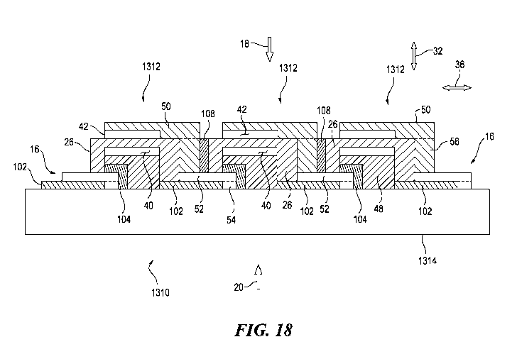
components
disposed on the side of ceramic seal 102 opposite of that of substrate 214.
In one form, ceramic seal 102 is positioned to prevent or reduce leakage of
gases and liquids from substrate 214 into interconnect 16. In one form,
ceramic seal
102 extends in direction 36, and is positioned vertically (in direction 32)
between porous
substrate 214 on the bottom and blind primary conductor 52 of interconnect 16
and
electrolyte 26 on the top, thereby preventing the leakages of gases and
liquids into the
portions of blind primary conductor 52 (and electrolyte 26) that are
overlapped by
29
CA 02838939 2013-12-10
WO 2012/174000 PCT/US2012/042066
ceramic seal 102. In other embodiments, ceramic seal 102 may be disposed in
other
suitable locations in addition to or in place of that illustrated in FIG. 7.
Blind primary
conductor 52 is embedded between a portion of ceramic seal 102 on the bottom
and a
portion of extended electrolyte 26 on the top. The diffusion distance in the
embodiment
of FIG. 7 is primarily defined by the length of the overlap of interconnect 16
by both
ceramic seal 102 and electrolyte 26 in direction 36. In one form, the overlap
is 0.3-0.6
mm, although in other embodiments, other values may be employed. Interconnect
16
extends into the active electrochemical cell 212 area. In some embodiments,
the
primary interconnect area of the configuration illustrated in FIG. 7 may be
smaller than
other designs, which may increase the total active cell area on substrate 214,
which
may increase the efficiency of fuel cell system 210.
Ceramic seal 102 is formed from a ceramic material. In one form, the ceramic
material used to form ceramic seal 102 is yittria stabilized zirconia, such as
3YSZ. In
another form, the material used to form ceramic seal 102 is scandia stabilized
zirconia,
such as 4ScSZ. In another form, the material used to form ceramic seal 102 is
alumina.
In another form, the material used to form ceramic seal 102 is non-conductive
PYrochlore materials, such as La2Zr207. Other embodiments may employ other
ceramics, e.g., depending upon various factors, such as compatibility with the
materials
of adjacent portions of each electrochemical cell 212 and substrate 214, the
fuels and
oxidants employed by fuel cell system 210, and the local transient and steady-
state
operating temperatures of fuel cell system 210. Still other embodiments may
employ
materials other than ceramics.
CA 02838939 2013-12-10
WO 2012/174000 PCT/US2012/042066
In the embodiment of FIG. 7, various features, components and
interrelationships
therebetween of aspects of an embodiment of the present invention are
depicted.
However, the present invention is not limited to the particular embodiment of
FIG. 7 and
the components, features and interrelationships therebetween as are
illustrated in FIG.
7 and described herein.
Referring to FIG. 8, some aspects of a non-limiting example of an embodiment
of
a fuel cell system 310 are schematically depicted. Fuel cell system 310
includes a
plurality of electrochemical cells 312 disposed on a substrate 314, each
electrochemical
cell 312 including a ceramic seal 102. Fuel cell system 310 also includes the
components set forth above and described with respect to fuel cell system 10,
e.g.,
including interconnects 16 having blind primary conductors 52 and blind
auxiliary
conductors or vias 54 and 56; an oxidant side 18; a fuel side 20; electrolyte
layers 26;
anodes 40; cathodes 42, anode conductor films 48 and cathode conductor films
50.
The description of substrate 14 applies equally to substrate 314. In the
embodiment of
FIG. 8, interconnect 16 is formed predominantly by the material of anode
conductor film
48, and hence, blind primary conductor 52 and auxiliary conductor 54 in the
embodiment of FIG. 8 may be considered as extensions of anode conductor film
48.
For example, blind primary conductor 52 and auxiliary conductor 54 are
depicted as
being formed by the material of anode conductor film 48, whereas auxiliary
conductor
56 is formed of the materials set forth above for interconnect 16 in the
embodiment of
FIG. 2. In one form, blind primary conductor 52 is in the form of a continuous
strip, e.g.,
continuous strip 52A depicted in FIG. 4A. In another form, blind primary
conductor 52 is
31
CA 02838939 2013-12-10
WO 2012/174000 PCT/US2012/042066
in the form of a plurality of vias, such as vias 52B in FIG. 4B. In other
embodiments,
blind primary conductor 52 may take other forms not explicitly set forth
herein.
Ceramic seal 102 is positioned to prevent or reduce leakage of gases and
liquids
from substrate 314 into interconnect 16. In one form, ceramic seal 102 is
positioned
vertically (in direction 32) between porous substrate 314 on the bottom and
blind
primary conductor 52 and electrolyte 26 on the top, thereby preventing the
leakages of
gases and liquids into the portions of blind primary conductor 52 that are
overlapped by
ceramic seal 102. Blind primary conductor 52 is embedded between a portion of
ceramic seal 102 on the bottom and extended electrolyte 26 on the top. The
diffusion
distance in the embodiment of FIG. 8 is primarily defined by the length of the
overlap of
interconnect 16 by both ceramic seal 102 and electrolyte 26 in direction 36.
In one
form, the overlap is 0.3-0.6 mm, although in other embodiments, other values
may be
employed.
Because ceramic seal 102 prevents the ingress of gas and liquids into
electrochemical cell 312, interconnect 16 does not need to be as dense (in
order to
prevent or reduce leakage) as other designs that do not include a seal, such
as ceramic
seal 102. In such designs, interconnect 16 may be formed of the materials used
to form
anode conductor layer 48 and/or cathode conductor layer 50. For example,
referring to
FIG. 9, an embodiment is depicted wherein interconnect 16 is formed entirely
of the
materials used to form anode conductor layer 48 and cathode conductor layer
50. FIG.
9 schematically depicts some aspects of a non-limiting example of an
embodiment of a
fuel cell system 410. Fuel cell system 410 includes a plurality of
electrochemical cells
412 disposed on a substrate 414, each electrochemical cell 412 including a
ceramic
32
CA 02838939 2013-12-10
WO 2012/174000 PCT/US2012/042066
seal 102. Fuel cell system 410 also includes the components set forth above
and
described with respect to fuel cell system 10, e.g., including interconnects
16 having
blind primary conductors 52 and blind auxiliary conductors or vias 54 and 56;
an oxidant
side 18; a fuel side 20; electrolyte layers 26; anodes 40; cathodes 42, anode
conductor
films 48 and cathode conductor films 50. The description of substrate 14
applies
equally to substrate 414. In the embodiment of FIG. 9, blind primary conductor
52 and
auxiliary conductor 54 are formed of the same material used to form anode
conductor
film 48, and are formed in the same process steps used to form anode conductor
film
48. Hence, blind primary conductor 52 and auxiliary conductor 54 in the
embodiment of
FIG. 9 may be considered as extensions of anode conductor film 48. Similarly,
in the
embodiment of FIG. 9, auxiliary conductor 56 is formed of the same material
used to
form cathode conductor film 50, and is formed in the same process steps used
to form
cathode conductor film 50. Hence, auxiliary conductor 56 in the embodiment of
FIG. 9
may be considered as an extension of cathode conductor film 50.
In the embodiments of FIGS. 8 and 9, various features, components and
interrelationships therebetween of aspects of embodiments of the present
invention are
depicted. However, the present invention is not limited to the particular
embodiments of
FIGS. 8 and 9 and the components, features and interrelationships therebetween
as are
illustrated in FIGS. 8 and 9 and described herein.
Referring to FIGS. 10-15 generally, the inventors have determined that
material
diffusion between the interconnect and adjacent components, e.g., an anode
and/or an
anode conductor film and/or cathode and/or cathode conductor film, may
adversely
affect the performance of certain fuel cell systems. Hence, some embodiments
of the
33
CA 02838939 2013-12-10
WO 2012/174000 PCT/US2012/042066
present invention include an electrically conductive chemical barrier (e.g.,
as discussed
above, and/or chemical barrier 104, discussed below with respect to FIGS. 10-
15) to
prevent or reduce such material diffusion. In various embodiments, chemical
barrier
104 may be configured to prevent or reduce material migration or diffusion at
the
interface between the interconnect and an anode, and and/or between the
interconnect
and an anode conductor film, and/or between the interconnect and a cathode,
and
and/or between the interconnect and a cathode conductor film which may improve
the
long term durability of the interconnect. For example, without a chemical
barrier,
material migration (diffusion) may take place at the interface between an
interconnect
formed of a precious metal cermet, and an anode conductor film and/or anode
formed
of a Ni-based cermet. The material migration may take place in both
directions, e.g., Ni
migrating from the anode conductive layer/conductor film and/or anode into the
interconnect, and precious metal migrating from the interconnect into the
conductive
layer/conductor film and/or anode. The material migration may result in
increased
porosity at or near the interface between the interconnect and the anode
conductor film
and/or anode, and may result in the enrichment of one or more non or low-
electronic
conducting phases at the interface, yielding a higher area specific resistance
(ASR),
and hence resulting in reduced fuel cell performance. Material migration
between the
interconnect and the cathode and/or between the interconnect and the cathode
conductor film may also or alternatively result in deleterious effects on fuel
cell
performance.
Accordingly, some embodiments employ a chemical barrier, e.g., chemical
barrier 104, that is configured to prevent or reduce material migration or
diffusion at the
34
CA 02838939 2013-12-10
WO 2012/174000 PCT/US2012/042066
interface between the interconnect and an adjacent electrically conductive
component,
such as one or more of an anode, an anode conductive layer/conductor film, a
cathode
and/or a cathode conductive layer/conductor film, and hence prevent or reduce
material
migration (diffusion) that might otherwise result in deleterious effect, e.g.,
the formation
of porosity and the enrichment of one or more non or low-electronic conducting
phases
at the interface. Chemical barrier 104 may be formed of one or both of two
classes of
materials; cermet and/or conductive ceramic. For the cermet, the ceramic phase
may
be one or more of an inert filler; a ceramic with low ionic conductivity, such
as YSZ; and
an electronic conductor. In various embodiments, e.g., for the anode side
(e.g., for use
adjacent to an anode and/or anode conductive layer/conductor film), chemical
barrier
104 may be formed of one or more materials, including, without limitation, Ni
cermet or
Ni-precious metal cermet. The precious metal phase may be, for example and
without
limitation, one or more of Ag, Au, Pd, Pt, or one or more alloys of Ag, Au, Pd
and/or Pt.
The ceramic phase in the cermet may be, for example and without limitation, be
at least
one of YSZ (such as 3YSZ), ScSZ (such as 4ScSZ), doped ceria (such as Gdo iCeo
9
02), SrZr03, pyrochlores of the composition (MRE)2Zr207 (where MRE = one or
more rare
earth cations, for example and without limitation La, Pr, Nd, Gd, Sm, Ho, Er,
and/or Yb),
for example and without limitation, La2Zr207 and Pr2Zr207, alumina, and Ti02,
or one or
more electronically conductive ceramics, such as doped ceria (higher
electronic
conductivity at lower oxygen partial pressure to provide low enough ASR due to
thin
film), doped strontium titanate, LSCM (La1_xSrxCr1_yMny03, x=0.15-0.35, y=0.25-
0.5),
and/or other doped lanthanum chromites and doped yttria chromites. In various
embodiments, e.g., for the cathode side(e.g., for use adjacent to a cathode
and/or
CA 02838939 2013-12-10
WO 2012/174000 PCT/US2012/042066
cathode conductive layer/conductor film), chemical barrier 104 may be formed
of one or
more materials, including, without limitation precious metal cermet. The
precious metal
phase may be, for example and without limitation, one or more of Ag, Au, Pd,
Pt, or one
or more alloys of Ag, Au, Pd and/or Pt. The ceramic phase in the cermet may
be, for
example and without limitation, be at least one of YSZ, ScSZ, doped ceria,
SrZr03,
pyrochlores of the composition (MRE)2Zr207(where MRE = one or more rare earth
cations, for example and without limitation La, Pr, Nd, Gd, Sm, Ho, Er, and/or
Yb), for
example and without limitation, La2Zr207 and Pr2Zr207, alumina, and Ti02, or
one or
more electronically conductive ceramics, such as LNF (LaNixFei_x03, such as
x=0.6)
LSM (Lai_xSrxMn03, x=0.15-0.3), LCM (such as Lao8Cao2Mn03), Ruddlesden-Popper
nickelates, LSF (such as Lao8Sro2Fe03), LSCF (Lao6Sro4C002Fe0803), LSCM
(LaiSrCr 1_yMny03, x=0.15-0.35, y=0.5-0.75) doped yttrium chromites, and other
doped
lanthanum chromites. The selection of the specific material(s) for chemical
barrier 104
may vary with the needs of the application, e.g., depending upon cost, ease of
manufacturing, the type of materials used for the component(s) electrically
adjacent to
interconnect 16 and/or one of its subcomponents, e.g., blind primary conductor
52,
auxiliary conductor 54 and auxiliary conductor 56.
One example of anode side chemical barrier materials is 15%Pd, 19%NiO,
66%NTZ, where NTZ is 73.6wt% NiO, 20.0%Ti02, 6.4% YSZ.
Another example of anode side chemical barrier materials is doped ceria, such
as GdoiCeo 9 02
Experimental testing with a chemical barrier, such as chemical barrier 104, in
a
fuel cell system yielded approximately 0.1% per thousand hour degradation rate
in cell
36
CA 02838939 2013-12-10
WO 2012/174000 PCT/US2012/042066
power output over the course of 1300 hours of testing using a chemical barrier
formed
of 30wt%Pd-70wt(YoNTZ cermet (NTZ = Ni02-3YSZ), disposed between an
interconnect
formed of 65Pd35Pt-YSZ cermet and an anode conductive layer formed of 20wt%Pd-
Ni-spinel. In a comparative test, but without the inclusion of a chemical
barrier, such as
chemical barrier 104, an interconnect formed of 50e0(96Pd6Au)-50e0YSZ cermet
directly interfacing with an anode conductive layer formed of 20wt%Pd-Ni-
spinel
showed significant degradation in about 10 hours of testing, and fuel cell
failure at about
25 hours of testing resulting from material migration between the interconnect
and the
anode conductive layer. In another test, two fuel cells were tested using a
chemical
barrier 104 formed of a conductive ceramic (10mor/oGd doped Ce02) disposed
between disposed between an anode conductor film and an interconnect. ASR for
the
interconnect showed no degradation after approximately 8000 hours of testing,
and
instead showed slight improvement, yielding final values of .05 ohm-cm2 and
.06 ohm-
cm2 in the two test articles.
Referring to FIG. 10, some aspects of a non-limiting example of an embodiment
of a fuel cell system 510 disposed on a substrate 514 are schematically
depicted. Fuel
cell system 510 includes a chemical barrier 104. Fuel cell system 510 also
includes
some the components set forth above and described with respect to fuel cell
system 10,
e.g., including an interconnects 16 having a blind primary conductor 52; an
oxidant side
18; a fuel side 20; electrolyte layers 26; anodes 40; and cathodes 42.
Although only a
single instance of interconnect 16, blind primary conductor 52, anode 40 and
cathode
42 are depicted, and two instances of electrolyte layers 26 are depicted, it
will be
understood that fuel cell system 510 may include a plurality of each such
components,
37
CA 02838939 2013-12-10
WO 2012/174000 PCT/US2012/042066
e.g., arranged in series in direction 36, e.g., similar to embodiments
described above.
The description of substrate 14 applies equally to substrate 514. In fuel cell
system
510, chemical barrier 104 is disposed between anode 40 and interconnect 16
(blind
primary conductor 52), extending in direction 32 between anode 40 and
interconnect 16,
and is configured to prevent material migration between anode 40 and
interconnect 16
(blind primary conductor 52). Chemical barrier 104 may be formed from one or
more of
the materials set forth above with respect to the embodiments of FIGS. 10-15.
Referring to FIG. 11, some aspects of a non-limiting example of an embodiment
of a fuel cell system 610 are schematically depicted. Fuel cell system 610
includes a
plurality of electrochemical cells 612 disposed on a substrate 614, each
electrochemical
cell 612 including a chemical barrier 104. Fuel cell system 610 also includes
the
components set forth above and described with respect to fuel cell system 10,
e.g.,
including interconnects 16 having blind primary conductors 52 and blind
auxiliary
conductors or vias 54 and 56; an oxidant side 18; a fuel side 20; electrolyte
layers 26;
anodes 40; cathodes 42, anode conductor films 48 and cathode conductor films
50.
The description of substrate 14 applies equally to substrate 614. In fuel cell
system
610, chemical barrier 104 is disposed between anode conductor film 48 and
interconnect 16 (blind primary conductor 52), extending in direction 32
between anode
conductor film 48 and interconnect 16, and is configured to prevent material
migration
between anode conductor film 48 and interconnect 16 (blind primary conductor
52).
Chemical barrier 104 may be formed from one or more of the materials set forth
above
with respect to the embodiments of FIGS. 10-15. In fuel cell system 610, a
portion of
38
CA 02838939 2013-12-10
WO 2012/174000 PCT/US2012/042066
electrolyte layer 26 is disposed between anode 40 and chemical barrier 104,
extending
in direction 36 between anode 40 and chemical barrier 104.
Referring to FIG. 12, some aspects of a non-limiting example of an embodiment
of a fuel cell system 710 are schematically depicted. Fuel cell system 710
includes a
plurality of electrochemical cells 712 disposed on a substrate 714, each
electrochemical
cell 712 including a ceramic seal 102 and a chemical barrier 104. Fuel cell
system 710
also includes the components set forth above and described with respect to
fuel cell
system 10, e.g., including interconnects 16 having blind primary conductors 52
and
blind auxiliary conductors or vias 54 and 56; an oxidant side 18; a fuel side
20;
electrolyte layers 26; anodes 40; cathodes 42, anode conductor films 48 and
cathode
conductor films 50. The description of substrate 14 applies equally to
substrate 714. In
fuel cell system 710, ceramic seal 102 is positioned to prevent or reduce
leakage of
gases and liquids from substrate 714 into interconnect 16 (blind interconnect
52), and
extends in direction 36 between the anode conductor film 48 of one
electrochemical cell
712 and the auxiliary conductor 54 of an adjacent electrochemical cell 712.
In fuel cell system 710, ceramic seal 102 is positioned vertically (in
direction 32)
between porous substrate 714 on the bottom and blind primary conductor 52 of
interconnect 16 and electrolyte 26 on the top, thereby preventing the leakages
of gases
and liquids from substrate 714 into the portions of blind primary conductor 52
(and
electrolyte 26) that are overlapped by ceramic seal 102. In other embodiments,
ceramic
seal 102 may be disposed in other suitable locations in addition to or in
place of that
illustrated in FIG. 12. Ceramic seal 102 may be formed of one or more of the
materials
set forth above with respect to the embodiment of FIG. 7. A portion of blind
primary
39
CA 02838939 2013-12-10
WO 2012/174000 PCT/US2012/042066
conductor 52 is embedded between ceramic seal 102 on the bottom and
electrolyte 26
on the top. The diffusion distance in the embodiment of FIG. 12 is primarily
defined by
the length of the overlap of blind primary conductor 52 by both ceramic seal
102 and
electrolyte 26 in direction 36.
In fuel cell system 710, chemical barrier 104 is disposed between anode
conductor film 48 and interconnect 16 (blind primary conductor 52), extending
in
direction 32 between anode conductor film 48 and both blind primary conductor
52 and
auxiliary conductor 54 of interconnect 16, and is configured to prevent
material
migration between anode conductor film 48 and blind primary conductor 52 and
auxiliary conductor 54. Chemical barrier 104 may be formed from one or more of
the
materials set forth above with respect to the embodiments of FIGS. 10-15.
Referring to FIG. 13, some aspects of a non-limiting example of an embodiment
of a fuel cell system 810 are schematically depicted. Fuel cell system 810
includes a
plurality of electrochemical cells 812 disposed on a substrate 814, each
electrochemical
cell 812 including a ceramic seal 102 and a chemical barrier 104. Fuel cell
system 810
also includes the components set forth above and described with respect to
fuel cell
system 10, e.g., including interconnects 16 having blind primary conductors 52
and
auxiliary conductors or vias 54 and 56; an oxidant side 18; a fuel side 20;
electrolyte
layers 26; anodes 40; cathodes 42, anode conductor films 48 and cathode
conductor
films 50. The description of substrate 14 applies equally to substrate 814.
In fuel cell system 810, ceramic seal 102 is positioned to prevent or reduce
leakage of gases and liquids from substrate 814 into interconnect 16 (blind
interconnect
52), and extends in direction 36 between the anode 40 and anode conductor film
48 of
CA 02838939 2013-12-10
WO 2012/174000 PCT/US2012/042066
one electrochemical cell 812 and the anode 40 and anode conductor film 48 of
an
adjacent electrochemical cell 812. In fuel cell system 810, ceramic seal 102
is
positioned vertically (in direction 32) between porous substrate 814 on the
bottom and
blind primary conductor 52 of interconnect 16 and electrolyte 26 on the top,
thereby
preventing the leakages of gases and liquids from substrate 714 into the
portions of
blind primary conductor 52 (and electrolyte 26) that are overlapped by ceramic
seal 102.
In other embodiments, ceramic seal 102 may be disposed in other suitable
locations in
addition to or in place of that illustrated in FIG. 13. Ceramic seal 102 may
be formed of
one or more of the materials set forth above with respect to the embodiment of
FIG. 7.
A portion of blind primary conductor 52 is embedded between ceramic seal 102
on the
bottom, and electrolyte 26 on the top. The diffusion distance in the
embodiment of FIG.
13 is primarily defined by the length of the overlap of blind primary
conductor 52 by both
ceramic seal 102 and electrolyte 26 in direction 36.
In fuel cell system 810, chemical barrier 104 is disposed between anode 40 and
blind primary conductor 52, and is configured to prevent material migration
between
anode 40 and blind primary conductor 52. In one form, chemical barrier 104
also
functions as auxiliary conductor 54. In other embodiments, auxiliary conductor
54 may
be formed separately from chemical barrier 104. Chemical barrier 104 may be
formed
from one or more of the materials set forth above with respect to the
embodiments of
FIGS. 10-15.
Referring to FIG. 14, some aspects of a non-limiting example of an embodiment
of a fuel cell system 910 disposed on a substrate 914 are schematically
depicted. Fuel
cell system 910 includes a chemical barrier 104. Fuel cell system 910 also
includes
41
CA 02838939 2013-12-10
WO 2012/174000 PCT/US2012/042066
some the components set forth above and described with respect to fuel cell
system 10,
e.g., including an interconnects 16 having a blind primary conductor 52; an
oxidant side
18; a fuel side 20; electrolyte layers 26; anodes 40; and cathodes 42.
Although only a
single instance of interconnect 16, blind primary conductor 52, anode 40 and
cathode
42 are depicted, and two instances of electrolyte layers 26 are depicted, it
will be
understood that fuel cell system 910 may include a plurality of each such
components,
e.g., arranged in series in direction 36, e.g., similar to embodiments
described above.
The description of substrate 14 applies equally to substrate 914. In fuel cell
system
910, chemical barrier 104 is disposed between cathode 42 and interconnect 16
(blind
primary conductor 52), extending in direction 32 between cathode 42 and
interconnect
16, and is configured to prevent material migration between cathode 42 and
interconnect 16 (blind primary conductor 52). Chemical barrier 104 may be
formed from
one or more of the materials set forth above with respect to the embodiments
of FIGS.
10-15.
Referring to FIG. 15, some aspects of a non-limiting example of an embodiment
of a fuel cell system 1010 are schematically depicted. Fuel cell system 1010
includes a
plurality of electrochemical cells 612 disposed on a substrate 1014, each
electrochemical cell 1012 including a chemical barrier 104. Fuel cell system
1010 also
includes the components set forth above and described with respect to fuel
cell system
10, e.g., including interconnects 16 having blind primary conductors 52 and
blind
auxiliary conductors or vias 54 and 56; an oxidant side 18; a fuel side 20;
electrolyte
layers 26; anodes 40; cathodes 42, anode conductor films 48 and cathode
conductor
films 50. The description of substrate 14 applies equally to substrate 1014.
In fuel cell
42
CA 02838939 2013-12-10
WO 2012/174000 PCT/US2012/042066
system 1010, chemical barrier 104 is disposed between cathode conductor film
50 and
interconnect 16 (blind primary conductor 52), extending in direction 32
between cathode
conductor film 50 and interconnect 16 (blind primary conductor 52), and is
configured to
prevent material migration between cathode conductor film 50 and interconnect
16
(blind primary conductor 52). Chemical barrier 104 may be formed from one or
more of
the materials set forth above with respect to the embodiments of FIGS. 10-15.
In the
embodiment of FIG. 15, chemical barrier 104 also functions as auxiliary
conductor 56.
In the embodiments of FIGS. 10-15, various features, components and
interrelationships therebetween of aspects of embodiments of the present
invention are
depicted. However, the present invention is not limited to the particular
embodiments of
FIGS. 10-15 and the components, features and interrelationships therebetween
as are
illustrated in FIGS. 10-15 and described herein.
Referring to FIGS. 16-19 generally, the inventors have determined that in some
fuel cells, under some operating conditions, the cathode conductive
layer/conductor
film, the electrolyte, and portions of the interconnect, e.g., vias, can form
parasitic cells
within or between each electrochemical cell, particularly where there is
overlap between
the cathode conductive layer/conductor film and the electrolyte. In the
parasitic cells,
the cathode conductive layer/conductor film functions as a cathode, and the
interconnect, e.g., vias formed of precious metal cermet, function as an
anode. The
parasitic cells consume fuel during fuel cell operation, thereby reducing the
efficiency of
the fuel cell system. In addition, the steam generated by the parasitic cells
may create
local high oxygen partial pressure that may result in the oxidation of Ni that
may have
43
CA 02838939 2013-12-10
WO 2012/174000 PCT/US2012/042066
diffused into precious metal phase of the interconnect (e.g., via) materials,
resulting in
degradation of the interconnect.
The inventors performed tests that confirmed the existence of parasitic cells.
The tests confirmed that, although significant degradation did not occur at
some
temperatures, e.g., 900 C, under the testing times, degradation of the
interconnect
occurred at higher operating temperatures, e.g., 925 C after approximately 700
hours of
testing. Post test analysis showed Ni migration from the anode conductive
layer/conductor film side to the cathode conductive layer/conductor film side
of the
interconnect through the precious metal phase in blind primary conductor 52,
which was
accelerated by the higher operating temperature. A high oxygen partial
pressure
resulting from steam formed by the parasitic cells caused Ni oxidation at the
interface of
extended electrolyte 26 and blind primary interconnect 52 near the boundary
between
the cathode conductive layer/conductor film and the electrolyte, which
segregated from
the precious metal of the interconnect. Continued NiO accumulation at the
interface
between the blind primary conductor 52 and the electrolyte 26, and continued
Ni
migration would likely result in failure of the interconnect.
In order to prevent overlap between the cathode conductive layer/conductor
film
and the electrolyte, in various embodiments the inventors employed a
separation
feature (gap 106 of FIGS. 16 and 17; and insulator 108 of FIGS. 18 and 19)
between
the cathode conductive layer/conductor film and the electrolyte to separate,
i.e., space
apart, the cathode conductive layer/conductor film and the electrolyte from
contacting
each other, thus eliminating the parasitic cells. Testing of fuel cell systems
with a
separation feature in the form of gap 106 (and also including a chemical
barrier 104
44
CA 02838939 2013-12-10
WO 2012/174000 PCT/US2012/042066
formed of Pd-Ni alloy cermet) for approximately 2000 hours, including
approximately
1000 hours at aggressive conditions (925 C and fuel consisting of 20% H2, 10%
CO,
19% CO2, 47% steam and 4% N2) did not result in degradation of the
interconnect.
Accordingly, some embodiments of the present invention include a separation
feature,
e.g., gap 106, between the cathode conductive layer/conductor film and the
electrolyte,
which prevents the establishment of parasitic cells.
Referring to FIG. 16, some aspects of a non-limiting example of an embodiment
of a fuel cell system 1110 are schematically depicted. Fuel cell system 1110
includes a
plurality of electrochemical cells 1112 disposed on a substrate 1114, each
electrochemical cell 1112 including a ceramic seal 102, a chemical barrier
104, and a
separation feature in the form of gap 106. Fuel cell system 1110 also includes
the
components set forth above and described with respect to fuel cell system 10,
e.g.,
including interconnects 16 having blind primary conductors 52 and blind
auxiliary
conductors or vias 54 and 56; an oxidant side 18; a fuel side 20; electrolyte
layers 26;
anodes 40; cathodes 42, anode conductor films 48 and cathode conductor films
50.
The description of substrate 14 applies equally to substrate 1114. Gap 106
extends in
direction 36 between cathode conductor film 50 (e.g., formed of one or more
cathode
conductive layers 30) and electrolyte layer 26.
In fuel cell system 1110, ceramic seal 102 is positioned to prevent or reduce
leakage of gases and liquids from substrate 1114 into interconnect 16 (blind
primary
conductor 52), and extends in direction 36 between the anode conductor film 48
of one
electrochemical cell 1112 and the auxiliary conductor 54 of an adjacent
electrochemical
cell 1112.
CA 02838939 2013-12-10
WO 2012/174000 PCT/US2012/042066
In fuel cell system 1110, ceramic seal 102 is positioned vertically (in
direction 32)
between porous substrate 1114 on the bottom and blind primary conductor 52 of
interconnect 16 and electrolyte 26 on the top, thereby preventing the leakages
of gases
and liquids from substrate 1114 into the portions of blind primary conductor
52 (and
electrolyte 26) that are overlapped by ceramic seal 102. In other embodiments,
ceramic
seal 102 may be disposed in other suitable locations in addition to or in
place of that
illustrated in FIG. 12. Ceramic seal 102 may be formed of one or more of the
materials
set forth above with respect to the embodiment of FIG. 7. A portion of blind
primary
conductor 52 is embedded between ceramic seal 102 on the bottom, and extended
electrolyte 26 on the top. The diffusion distance in the embodiment of FIG. 16
is
primarily defined by the length of the overlap of blind primary conductor 52
by both
ceramic seal 102 and electrolyte 26 in direction 36.
In fuel cell system 1110, chemical barrier 104 is disposed between anode
conductor film 48 and interconnect 16 (blind primary conductor 52), extending
in
direction 32 between anode conductor film 48 and both blind primary conductor
52 and
auxiliary conductor 54 of interconnect 16, and is configured to prevent
material
migration between anode conductor film 48 and blind primary conductor 52 and
auxiliary conductor 54. Chemical barrier 104 may be formed from one or more of
the
materials set forth above with respect to the embodiments of FIGS. 10-15.
In fuel cell system 1110, gap 106 is configured to prevent formation of a
parasitic
fuel cell between cathode conductor film 50, electrolyte layer 26 and blind
primary
conductor 52. Although gap 106 in the embodiment of FIG. 16 is employed in
conjunction with a fuel cell system having ceramic seal 102, chemical barrier
104 and
46
CA 02838939 2013-12-10
WO 2012/174000 PCT/US2012/042066
anode conductor film 48, in other embodiments, gap 106 may be employed in fuel
cell
systems that do not include components corresponding to one or more of ceramic
seal
102, chemical barrier 104 and anode conductor film 48.
Referring to FIG. 17, some aspects of a non-limiting example of an embodiment
of a fuel cell system 1210 are schematically depicted. Fuel cell system 1210
includes a
plurality of electrochemical cells 1212 disposed on a substrate 1214, each
electrochemical cell 1212 including a chemical barrier 104 and a separation
feature in
the form of gap 106. Fuel cell system 1210 also includes the components set
forth
above and described with respect to fuel cell system 10, e.g., including
interconnects 16
having blind primary conductors 52 and blind auxiliary conductors or vias 54
and 56; an
oxidant side 18; a fuel side 20; electrolyte layers 26; anodes 40; cathodes
42, anode
conductor films 48 and cathode conductor films 50. The description of
substrate 14
applies equally to substrate 1214.
In fuel cell system 1210, chemical barrier 104 is disposed between anode
conductor film 48 and interconnect 16 (blind primary conductor 52), extending
in
direction 32 between anode conductor film 48 and interconnect 16, and is
configured to
prevent material migration between anode conductor film 48 and interconnect 16
(blind
primary conductor 52). Chemical barrier 104 may be formed from one or more of
the
materials set forth above with respect to the embodiments of FIGS. 10-15. In
fuel cell
system 1210, a portion of electrolyte layer 26 is disposed between anode 40
and
chemical barrier 104, extending in direction 36 between anode 40 and chemical
barrier
104.
47
CA 02838939 2013-12-10
WO 2012/174000 PCT/US2012/042066
In fuel cell system 1210, gap 106 is configured to prevent formation of a
parasitic
fuel cell between auxiliary conductor 56 (formed of the same material as
cathode
conductor film 50), electrolyte layer 26 and blind primary conductor 52.
Although gap
106 in the embodiment of FIG. 17 is employed in conjunction with a fuel cell
system
having chemical barrier 104 and anode conductor film 48, in other embodiments,
gap
106 may be employed in fuel cell systems that do not include components
corresponding to one or more of chemical barrier 104 and anode conductor film
48.
Referring to FIG. 18, some aspects of a non-limiting example of an embodiment
of a fuel cell system 1310 are schematically depicted. Fuel cell system 1310
includes a
plurality of electrochemical cells 1312 disposed on a substrate 1314, each
electrochemical cell 1312 including a ceramic seal 102, a chemical barrier
104, and a
separation feature in the form of an insulator 108. Fuel cell system 1310 also
includes
the components set forth above and described with respect to fuel cell system
10, e.g.,
including interconnects 16 having blind primary conductors 52 and blind
auxiliary
conductors or vias 54 and 56; an oxidant side 18; a fuel side 20; electrolyte
layers 26;
anodes 40; cathodes 42, anode conductor films 48 and cathode conductor films
50.
The description of substrate 14 applies equally to substrate 1314. Insulator
108
extends in direction 36 between cathode conductor film 50 (e.g., formed of one
or more
cathode conductive layers 30) and electrolyte layer 26.
In fuel cell system 1310, ceramic seal 102 is positioned to prevent or reduce
leakage of gases and liquids from substrate 1314 into interconnect 16 (blind
primary
conductor 52), and extends in direction 36 between the anode conductor film 48
of one
48
CA 02838939 2013-12-10
WO 2012/174000 PCT/US2012/042066
electrochemical cell 1312 and the auxiliary conductor 54 of an adjacent
electrochemical
cell 1312.
In fuel cell system 1310, ceramic seal 102 is positioned vertically (in
direction 32)
between porous substrate 1314 on the bottom and blind primary conductor 52 of
interconnect 16 and electrolyte 26 on the top, thereby preventing the leakages
of gases
and liquids from substrate 1314 into the portions of blind primary conductor
52 (and
electrolyte 26) that are overlapped by ceramic seal 102. In other embodiments,
ceramic
seal 102 may be disposed in other suitable locations in addition to or in
place of that
illustrated in FIG. 12. Ceramic seal 102 may be formed of one or more of the
materials
set forth above with respect to the embodiment of FIG. 7. A portion of blind
primary
conductor 52 is embedded between ceramic seal 102 on the bottom, and extended
electrolyte 26 on the top. The diffusion distance in the embodiment of FIG. 18
is
primarily defined by the length of the overlap of blind primary conductor 52
by both
ceramic seal 102 and electrolyte 26 in direction 36.
In fuel cell system 1310, chemical barrier 104 is disposed between anode
conductor film 48 and interconnect 16 (blind primary conductor 52), extending
in
direction 32 between anode conductor film 48 and both blind primary conductor
52 and
auxiliary conductor 54 of interconnect 16, and is configured to prevent
material
migration between anode conductor film 48 and blind primary conductor 52 and
auxiliary conductor 54. Chemical barrier 104 may be formed from one or more of
the
materials set forth above with respect to the embodiments of FIGS. 10-15.
In fuel cell system 1310, insulator 108 is configured to prevent formation of
a
parasitic fuel cell between cathode conductor film 50, electrolyte layer 26
and blind
49
CA 02838939 2013-12-10
WO 2012/174000 PCT/US2012/042066
primary conductor 52. In one form, insulator 108 is formed from an insulating
non-
conductive materials, such as aluminum oxide (A1203), pyrochlore, such as In
other
embodiments, La2Zr207, Pr2Zr207, and SrZr03.other materials may be employed to
form
insulator 108, e.g., one or more other types of non-conducting ceramics in
addition to or
in place of aluminum oxide. Although insulator 108 in the embodiment of FIG.
16 is
employed in conjunction with a fuel cell system having ceramic seal 102,
chemical
barrier 104 and anode conductor film 48, in other embodiments, insulator 108
may be
employed in fuel cell systems that do not include components corresponding to
one or
more of ceramic seal 102, chemical barrier 104 and anode conductor film 48.
Referring to FIG. 19, some aspects of a non-limiting example of an embodiment
of a fuel cell system 1410 are schematically depicted. Fuel cell system 1410
includes a
plurality of electrochemical cells 1412 disposed on a substrate 1414, each
electrochemical cell 1412 including a chemical barrier 104 and a separation
feature in
the form of insulator 108. Fuel cell system 1410 also includes the components
set forth
above and described with respect to fuel cell system 10, e.g., including
interconnects 16
having blind primary conductors 52 and blind auxiliary conductors or vias 54
and 56; an
oxidant side 18; a fuel side 20; electrolyte layers 26; anodes 40; cathodes
42, anode
conductor films 48 and cathode conductor films 50. The description of
substrate 14
applies equally to substrate 1414.
In fuel cell system 1410, chemical barrier 104 is disposed between anode
conductor film 48 and interconnect 16 (blind primary conductor 52), extending
in
direction 32 between anode conductor film 48 and interconnect 16, and is
configured to
prevent material migration between anode conductor film 48 and interconnect 16
(blind
CA 02838939 2013-12-10
WO 2012/174000 PCT/US2012/042066
primary conductor 52). Chemical barrier 104 may be formed from one or more of
the
materials set forth above with respect to the embodiments of FIGS. 10-15. In
fuel cell
system 1410, a portion of electrolyte layer 26 is disposed between anode 40
and
chemical barrier 104, extending in direction 36 between anode 40 and chemical
barrier
104.
In fuel cell system 1410, insulator 108 is configured to prevent formation of
a
parasitic fuel cell between auxiliary conductor 56 (formed of the same
material as
cathode conductor film 50), electrolyte layer 26 and blind primary conductor
52.
Insulator 108 may be formed of the materials set forth above in the embodiment
of FIG.
18. Although insulator 108 in the embodiment of FIG. 19 is employed in
conjunction
with a fuel cell system having chemical barrier 104 and anode conductor film
48, in
other embodiments, insulator 108 may be employed in fuel cell systems that do
not
include components corresponding to one or more of chemical barrier 104 and
anode
conductor film 48.
In the embodiments of FIGS. 16-19, various features, components and
interrelationships therebetween of aspects of embodiments of the present
invention are
depicted. However, the present invention is not limited to the particular
embodiments of
FIGS. 16-19 and the components, features and interrelationships therebetween
as are
illustrated in FIGS. 16-19 and described herein.
As mentioned above with respect to FIGS. 16-19, under certain conditions,
parasitic cells may be undesirably formed. The embodiments discussed above
with
respect to FIGS. 16-19 provide certain approaches to resolving the parasitic
cell
problem. The inventors have also created other approaches to solving the
parasitic cell
51
CA 02838939 2013-12-10
WO 2012/174000 PCT/US2012/042066
problem, based on material selection, e.g., the material from which the
interconnect
and/or vias (e.g., interconnect 16, including blind primary conductor 52,
auxiliary
conductor 54 and/or auxiliary conductor 56, and/or other interconnect and/or
via
configurations not mentioned herein) are formed. In one form, for an alternate
cermet
material, precious metal- La2Zr207 Pyrochlore cermet may be employed for
primary
interconnect material for segmented-in-series fuel cell, or via material for
multi-layer
ceramic interconnect. In the such a cermet material, La2Zr207 Pyrochlore could
fully
replace doped zirconia, or partially replace doped zirconia to keep ionic
phase below its
percolation to eliminate or reduce ionic conduction.
In one form, the composition of the interconnect and/or via(s), e.g., one or
more
of the previously mentioned compositions for the interconnect and/or via(s),
is altered to
include non-ionic conducting ceramic phases in the composition of the
interconnect
and/or via(s).
For example, in one form, the interconnect and/or via may be formed, all or in
part, of a cermet, such as those previously described with respect to
interconnect 16,
including blind primary conductor 52, auxiliary conductor 54 and/or auxiliary
conductor
56, but also or alternatively including one or more non-ionic conductive
ceramic phases.
Examples include, without limitation, SrZr03, La2Zr207 Pyrochlore,
Pr2Zr207pyrochlore,
BaZr03, MgA1204 spinel, NiA1204 spinel, MgCr204 spinel, NiCr204 spinel,
Y3A15012 and
other garnets with various A- and B-site substitution, and alumina. Other non-
ionic
conductive ceramic phases are also contemplated herein in addition to or in
place of the
examples set forth herein. Considerations for materials may include the
coefficient of
thermal expansion of the ceramic phase(s), e.g., relative to the coefficient
thermal
52
CA 02838939 2013-12-10
WO 2012/174000 PCT/US2012/042066
expansion of the porous substrate. In some embodiments, preferred materials
for
chemical compatibility with adjacent fuel cell layers may include precious
metal-
pyrochlore cermets, wherein the general class of pyrochlores is (MRE)2Zr207,
wherein
MRE is a rare earth cation, for example and without limtiation La, Pr, Nd, Gd,
Sm, Ho, Er,
and/or Yb.
In other embodiments, nonionic phases such as SrZr03, MgA1204 spinel, NiA1204
spinel, alumina and pyrochlore compositions partially or completely replace
the ionic
conducting YSZ, e.g., of previously described interconnects and/or vias.
Preferably,
pyrochlore powders and/or one or more of the other nonionic phases replace YSZ
sufficiently to render the balance of the YSZ to be below a percolation
threshold to
eliminate ionic conductivity across the interconnect/via. The YSZ volume
fraction of the
via is purposely reduced to less than 30v% to minimize any ionic conductivity
within the
via material.
In one form, the composition of the interconnect and/or via(s), e.g., one or
more
of the previously mentioned compositions for the interconnect and/or via(s),
is altered to
include a reactant phase to form non-ionic conducting ceramic phases during
firing of
the fuel cell, e.g., by the inclusion of rare earth oxides in the compound
used to form the
interconnect/via(s).
For example, in some embodiments, all or portions interconnect 16 or other
interconnects or vias may include a reactant phase in the form of rare earth
oxide, e.g.,
within the screen printing ink, at less than the stoichiometric ratio to form
pyrochlore
being one mole of the oxides of La, Pr, Nd, Gd, Sm, Ho, Er, Yb to two moles of
the
zirconia content of the via. In the overall cermet composition (e.g., cermet
compositions
53
CA 02838939 2013-12-10
WO 2012/174000 PCT/US2012/042066
for all or part of interconnect 16 set forth herein) which reacts with the YSZ
during firing
of the fuel cell to form pyrochlore within the interconnect/via and adjacent
to the
electrolyte, e.g., electrolyte 26. In one form, the minimum rare earth oxide
required is
about 13mole% ceramic composition in order to reduce YSZ phase below 30v%
percolation. In other embodiments, other rare earth oxide amounts may be
employed.
The zirconia phase may still be able to exist at greater than the percolation
threshold,
since the insulating pyrochlore phase could form along grain boundaries.
However, in
some embodiments, it would be preferable to add sufficient rare earth oxides
to take the
YSZ phase content to below the percolation threshold on a bulk composition
basis.
Similar to the pyrochlores, SrZr03 nonionic phases could be created in-situ
through
addition of Sr0 powder as a reactant phase, e.g., to the interconnect inks, at
less than
the stoichimetric ratio of 1 mole Sr0 to 1 mole Zr02.
In still other embodiments, all or portions interconnect 16 or other
interconnects
or vias may include a content of rare earth oxide, e.g., within the screen
printing ink, at
greater than the stoichiometric ratio of pyrochlore being one mole of the
oxides, e.g., of
La, Pr, Nd, Gd, Sm, Ho, Er, and/or Yb, to two moles of the zirconia content of
the via in
the overall cermet composition (e.g., cermet compositions for all or part of
interconnect
16 set forth herein) which reacts with the YSZ during firing of the fuel cell
to form
pyrochlore within the interconnect/via, and the unreacted rare earth oxide
will further
react with the extended electrolyte in the vicinity of the interconnect during
electrolyte
firing to form a pyrochlore film on the electrolyte surface, e.g., on the
surface of
electrolyte 26, which will sufficiently disrupt the pathways for oxygen ionic
conductivity.
In form, the rare earth oxide amount is from 33mole% to 50mole% based on the
total
54
CA 02838939 2013-12-10
WO 2012/174000 PCT/US2012/042066
ceramic phase. In other embodiments, other rare earth oxide amounts may be
employed. The excess rare earth oxide may ensure the absence of ionic
conductivity.
However, too much excess rare earth remaining within the interconnect/via
could cause
the via to be susceptible to moisture induced damage on phase change to the
rare earth
hydroxides. Hence, it is desirable in some embodiments to limit the amount of
rare
earth oxides to less than 10% over the stoichiometric ratio. Similar to the
pyrochlores,
SrZr03 nonionic phases could be created in-situ within the via and adjacent
extended
electrolyte through addition of Sr0 powder to the interconnect inks in excess
of the
stoichimetric ratio of 1 mole Sr0 to 1 mole Zr02. In one form, a lower limit
is
approximately 15-20 mole% Sr0 based on the ceramic phase, in order to form
SrZr03
to reduce YSZ below the percolation threshold. In other embodiments, other
lower
limits may apply. In one form, an upper limit is about 50-60 mole% Sr0 based
on the
ceramic phase (Sr0 + Zr02). In other embodiments, other upper limits may
apply.
In yet still other embodiments, all or portions interconnect 16 or other
interconnects or vias may include a content of rare earth oxide at the
stoichiometric ratio
with YSZ to lead to full reactivity to (MRE)2Zr207.
Firing temperatures for using a reactant phase to form the non-ionic
conducting
ceramic phases during firing of the fuel cell may vary with the needs of the
particular
application. Considerations include, for example and without limitation, the
sinterability
of different materials, powder particle size, specific surface area. Other
material and/or
processing parameters may also affect the selected firing temperature. For
example, If
the temperature is too low, the electrolyte may have higher porosity and cause
leakage.
If the temperature is too high, it may cause other issues, such as too high an
anode
CA 02838939 2013-12-10
WO 2012/174000 PCT/US2012/042066
density, which may reduce electrochemical activity, or may cause substrate
dimensional
changes, etc. Hence, the actual firing temperature for purposes of using one
or more
reactant phases to form one or more non-ionic conducting ceramic phases may
vary as
between applications. In one form, the firing temperature may be 1385 C. In
some
embodiments, the firing temperature may be in the range of 1370 C to 1395 C.
In other
embodiments, the firing temperature may be in the range of 1350 C to 1450 C.
In still
other embodiments, the firing temperature may be outside the range of 1350 C
to
1450 C. Processing steps to form the one or more non-ionic conducting ceramic
phases may include preparing a composition including the rare earth oxide, YSZ
and a
precious metal, forming the interconnect/via(s), firing the composition at the
desired
temperature, e.g., at a temperature or within a temperature range set forth
above, and
holding the composition at the firing temperature for a desired period, e.g.,
in the range
of 1-5 hours. In embodiments wherein all or portions of the fuel cell are
formed by
screen printing, the method may include preparing a screen printable ink that
incorporates the rare earth oxide, YSZ and the precious metal; printing the
interconnect/via(s); drying the ink; firing the printed interconnect/via(s) at
the desired
temperature, e.g., at a temperature or within a temperature range set forth
above; and
holding the composition at the firing temperature for a desired period, e.g.,
in the range
of 1-5 hours.
In additional embodiments, other non-ionic conducting phases or reactant
phases may be employed to minimize the ionic conductivity of the interconnect.
The following Tables 1-8 provide compositional information for some aspects of
non-limiting experimental fuel cell and fuel cell component examples produced
in
56
CA 02838939 2013-12-10
WO 2012/174000
PCT/US2012/042066
accordance with some aspects of some embodiments of the present invention. It
will be
understood the present invention is in no way limited to the examples provided
below.
The columns entitled "General Composition" illustrate some potential
compositional
ranges, including some preferred ranges, for some materials described herein,
whereas, the columns entitled "Specific Composition" illustrates the materials
used in
the test articles/materials.
TABLE 1 (w/o ceramic seal)
General Composition
Specific Composition
Anode NiO-YSZ (Ni0=55-75wt%)
Anode conductive layer Pd-Ni-YSZ
Cathode Laii_.)Sr.Mn0(3D(x=0.1-0.3) -3YSZ
Cathode conductive layer Pd - Laii_.)Sr.Mn0(3_,0 (x=0.1-0.3)
Electrolyte 3YSZ 3YSZ
Blind primary conductor xPd(100-x)Pt -YSZ (x=35-65 wt ratio, 31.1%Pd,
31.1%Pt, 24.4% 3YSZ
alloy is 35-80v%)
Auxiliary conductor on anode side xPd(100-x)Pt -YSZ (x=35-65 wt ratio,
31.1%Pd, 31.1%Pt, 24.4% 3YSZ
alloy is 35-80v%)
Auxiliary conductor on cathode side Pd - Laii_.)Sr.Mn0(3_,0 (x=0.1-0.3)
Substrate MgO-MgA1204 69.4%Mg0,
30.6%MgA1204
Substrate surface modification layer 3-8
mol%Y203-Zr02 8YSZ
Ceramic seal N/A N/A
Cell ASR, ohm-cm^2 0.375
Interconnect ASR, ohm-cm^2 0.027
Test duration, hrs 860
Examples: TCT23 (STC13-3):
blind primary interconnect
is long strip design
Figure 4
57
CA 02838939 2013-12-10
WO 2012/174000
PCT/US2012/042066
TABLE 2 (w/o ceramic seal)
General Composition
Specific Composition
Anode NiO-YSZ (Ni0=55-75wt%)
Anode conductive layer Pd-Ni-YSZ
Cathode Laii,)Sr.Mn0(3_d)(x=0.1-0.3) -3YSZ
Cathode conductive layer Pd - La(1,)Sr.Mn0(3_d) (x=0.1-0.3)
Electrolyte 3YSZ 3YSZ
Blind primary conductor xPd(100-x)Pt -YSZ (x=35-65 wt ratio, 31.1%Pd,
31.1%Pt, 24.4% 3YSZ
alloy is 35-80v%)
Auxiliary conductor on anode side xPd(100-x)Pt -YSZ (x=35-65 wt ratio,
31.1%Pd, 31.1%Pt, 24.4% 3YSZ
alloy is 35-80v%)
Pd - La(1,)Sr.Mn0(3_d) (x=0.1-0.3)
Substrate MgO-MgA1204 69.4%Mg0,
30.6%MgA1204
Substrate surface modification layer 3-8
mol%Y203-Zr02 8YSZ
Ceramic seal N/A
cell ASR, ohm-cm^2 0.30
Interconnect ASR, ohm-cm^2 0.02
Test duration, hrs 3500
Examples: PCT11(PC08-2/3):
blind primary interconnect
is via design
Figure 6
58
CA 02838939 2013-12-10
WO 2012/174000
PCT/US2012/042066
TABLE 3 (with ceramic seal)
General Composition
Specific Composition
Anode NiO-YSZ (Ni0=55-75wt%)
Anode conductive layer Pd-Ni-YSZ
Cathode La(l_x)SrxMn0(3_3)(x=0.1-0.3) -3YSZ
Cathode conductive layer Pd - La(l,)SrxMl10(3-5) (x=0.1-0.3)
Electrolyte 3YSZ 3YSZ
Blind primary conductor Pd-Ni-YSZ
76.5%Pd, 8.5%Ni, 15%3YSZ
Auxiliary conductor on anode side Pd-Ni-YSZ
76.5%Pd, 8.5%Ni, 15%3YSZ
Auxiliary conductor on cathode side Pd - La(i_x)SrxMn0(3_3) (x=0.1-0.3)
Substrate MgO-MgA1204
69.4%Mg0, 30.6%MgA1204
Substrate surface modification layer 3-8
mol%Y203-Zr02 8YSZ
Ceramic seal 3-5 mol%Y203-Zr02, or 3YSZ
4-6mol%5c203-Zr02
cell & interconnect ASR, ohm-cm^2 0.50
Test duration, hrs 1200
Examples: TCT2: blind primary
interconnect is long strip design
Figure 8
59
CA 02838939 2013-12-10
WO 2012/174000
PCT/US2012/042066
TABLE 4 (Pd-NTZ as chemical barrier)
General Composition
Specific Composition
knode NiO-YSZ (Ni0=55-75wt%)
knode conductive layer Pd-Ni0-(Mg0.4.2,
Ni0.58)A1204.
Dathode La(l_x)Sr,<Mn0(3-5)(x=0.1-0.3) -3YSZ
Dathode conductive layer La(l_x)SrxMn0(3_d) (x=0.1-
0.3)
Electrolyte 3-8 mol%Y203-Zr02, or
4-11 mol%Sc203-Zr02 3YSZ
3Iind primary conductor xPd(100-x)Pt -YSZ (x=35-65 wt ratio,
31.1%Pd, 31.1%Pt, 24.4% 3YSZ
alloy is 35-80v%)
Dhemical barrier on anode side xPd-(100-x) NTZ* (x=10-40)
15%Pd, 19%NiO, 66%NTZ
kuxiliary conductor on La(1-x)SrxMn0(3-d) (x=0.1-0.3)
.:athode side
3ubstrate MgO-MgA1204
69.4%Mg0, 30.6%MgA1204
-Substrate surface 3-8 mol%Y203-Zr02 8YSZ
nodification layer
Deramic seal N/A N/A
ell ASR, ohm-cm^2 0.35
nterconnect ASR, ohm-cm^2 0.02-
0.05
fest duration, hrs 1400
NTZ: 73.6wt% NiO, 20.0%Ti02,
3.4% YSZ
Examples: PCT14B (PC11-4),
And vies, Fig. 11
CA 02838939 2013-12-10
WO 2012/174000
PCT/US2012/042066
TABLE 5, wt% (GDC10 as chemical barrier)
General Composition Specific
Composition
knode NiO-YSZ (Ni0=55-75wt%)
knode conductive layer Pd-NiO-(Mg0.4.2, Nlo.58)A1204.
3athode Lam,)Sr,<Mn0(3-5)(x=0.1-0.3) -3YSZ
3athode conductive layer Lam,)SrxMn0(3-d)(x=0.1-0.3)
Electrolyte 3-8 mol%Y203-Zr02, or 3YSZ
4-11 mol%5c203-Zr02
3Iind primary conductor xPd -(100-x)YSZ (x=70-90 weight ratio) 85%Pd,
15%3YSZ
3hemical barrier on anode side Doped Ceria
(Gdai,Ceo.9)02
kuxiliary conductor on La(1,)SrxMn0(3_d)(x=0.1-0.3)
:athode side
iubstrate MgO-MgA1204
69.4%Mg0, 30.6%MgA1204
iubstrate surface 3-8 mol%Y203-Zr02 8YSZ
nodification layer
3eramic seal 3-5 mol%Y203-Zr02, or 3YSZ
4-6mol%5c203-Zr02
3ell ASR, ohm-cm^2 0.24
nterconnect ASR, ohm-cm^2 0.04-
0.05
-est duration, hrs 1340
Examples: PCT55A (PC28-2)
or Fig. 12
61
CA 02838939 2013-12-10
WO 2012/174000
PCT/US2012/042066
TABLE 6, wt%
General Composition
Specific Composition
Anode NiO-YSZ (Ni0=55-75wt%)
Anode conductive layer Pd-NiO-(Mg0.4.2, Nlo.58)A1204.
Cathode Lam,)Sr,<Mn0(3-5)(x=0.1-0.3) -3YSZ
Cathode conductive layer La(1,)SrxMn0(3_d)(x=0.1-0.3), or
LaNi0.6Fe0.403
Electrolyte 4-11 mol% Sc203-Zr02 6ScSZ
Blind primary conductor xPd(100-x)Pt -YSZ (x=35-65 wt ratio,
31.1%Pd, 31.1%Pt, 24.4% 3YSZ
alloy is 35-80v%)
Chemical barrier on anode side Doped Ceria (Gd0i,Ce0.9)02
Auxiliary conductor on La(1,)SrxMn0(3_d)(x=0.1-0.3), or
cathode side LaNi0.6Fe0.403
Substrate MgO-MgA1204
69.4%Mg0, 30.6%MgA1204
Substrate surface 3-8 mol%Y203-Zr02 8YSZ
modification layer
Ceramic seal 3-5 mol%Y203-Zr02, or 3YSZ
4-6mol%5c203-Zr02
Cell ASR, ohm-cm^2 0.24
Interconnect ASR, ohm-cm^2 0.05-
0.06
Test duration, hrs 8000
Examples: PCT63A&B
For Figiure 16
62
CA 02838939 2013-12-10
WO 2012/174000 PCT/US2012/042066
TABLE 7
General Composition Specific Composition
Anode
Anode conductive layer
Cathode
Cathode conductive layer
Electrolyte
Blind primary conductor Pt-YSZ-SrZr03
78.8%Pt-11.1%3YSZ-10.1%SrZr03
Auxiliary conductor on anode side
Auxiliary conductor on cathode side
Substrate
Substrate surface modification layer
Ceramic seal
Cell ASR, ohm-cm^2
Interconnect ASR, ohm-cm^2
Examples: not tested in an actual
SOFC test article, pellet formulation
63
CA 02838939 2013-12-10
WO 2012/174000
PCT/US2012/042066
TABLE 8
General Composition
Specific Composition
Anode NiO-YSZ (Ni0=55-75wt%)
Anode conductive layer Pd-Ni0-(Mg0.4.2, Nlo.58)A1204.
Cathode Lam,)Sr,<Mn0(3-5)(x=0.1-0.3) -3YSZ
Cathode conductive layer Lam_x)SrxMn0(3-d) (x=0.1-0.3)
Electrolyte 3-8 mol%Y203-Zr02 3YSZ
Blind primary conductor Pt-Pd-YSZ-La203 36%Pt-36%Pd-25.2%3YSZ-
2.8%La203
Auxiliary conductor on anode side Pt-Pd-YSZ-La203 36%Pt-36%Pd-25.2%3YSZ-
2.8%La203
Auxiliary conductor on La(i_x)SrxMn0(3_d) (x=0.1-0.3)
cathode side
Substrate MgO-MgA1204 69.4%Mg0,
30.6%MgA1204
Substrate surface 3-8 mol%Y203-Zr02 8YSZ
modification layer
Ceramic seal 3-5 mol%Y203-Zr02, or 3YSZ
4-6mol%5c203-Zr02
Cell ASR, ohm-cm^2 0.3-0.34
Interconnect ASR, ohm-cm^2 0.04-0.07
Examples: PCT57
Embodiments of the present invention include a fuel cell system, comprising:a
plurality of electrochemical cells, each electrochemical cell formed of an
anode, a
cathode spaced apart from the anode, and an electrolyte disposed between the
anode
and the cathode; an interconnect electrically coupling a pair of electrically
adjacent
electrochemical cells, the interconnect electrically coupling the anode of one
electrochemical cell to the cathode of the other electrochemical cell; and a
cathode
conductive layer electrically coupled to the interconnect, wherein the
interconnect is in
contact with the cathode conductive layer and in contact with the electrolyte;
and
wherein the interconnect is formed of a cermet compound having a reactant
phase
configured for in-situ formation of at least one non-ionic conducting ceramic
phase
during firing of the fuel cell system.
In a refinement, the cermet compound include yttria stabilized zirconia (YSZ).
64
CA 02838939 2013-12-10
WO 2012/174000 PCT/US2012/042066
In another refinement, the reactant phase is Sr0.
In yet another refinement, the reactant phase is configured to form a SrZr03
non-
ionic conducting phase during the firing.
In still another refinement, the reactant phase is a rare earth oxide.
In yet still another refinement, the rare earth oxide is an oxide of at least
one of
La, Pr, Nd, Gd, Sm, Ho, Er and Yb.
In a further refinement, the reactant phase is configured to form a pyrochlore
non-ionic conducting phase during the firing.
In a yet further refinement, the amount of the reactant phase is less than the
stoichiometric ratio with the YSZ to form the non-ionic conducting phase.
In a still further refinement, the amount of the reactant phase is at the
stoichiometric ratio with the YSZ to form the non-ionic conducting phase.
In a yet still further refinement, the amount of the reactant phase is greater
than
the stoichiometric ratio with the YSZ to form the non-ionic conducting phase.
In another further refinement, the cathode conductive layer is in contact with
the
electrolyte.
In yet another further refinement, the interconnect includes a portion
embedded
within the electrolyte.
Embodiments of the present invention include a fuel cell system, comprising: a
cathode of a first electrochemical cell; an electrolyte; and an anode of a
second
electrochemical cell spaced apart from the cathode by the electrolyte; a
cathode
CA 02838939 2013-12-10
WO 2012/174000 PCT/US2012/042066
conductive layer adjoining the cathode; an interconnect configured to conduct
free
electrons between the anode and the cathode, wherein the interconnect adjoins
both
the cathode conductive layer and the electrolyte; and wherein the interconnect
is formed
of a cermet compound having a reactant phase configured for in-situ formation
of at
least one non-ionic conducting ceramic phase during firing of the fuel cell
system.
In a refinement, the cermet compound include yttria stabilized zirconia (YSZ).
In another refinement, the reactant phase is Sr0.
In yet another refinement, the reactant phase is configured to form a SrZr03
non-
ionic conducting phase during the firing.
In a further refinement, the reactant phase is a rare earth oxide.
In a yet further refinement, the rare earth oxide is an oxide of at least one
of La,
Pr, Nd, Gd, Sm, Ho, Er and Yb.
In a still further refinement, the reactant phase is configured to form a
pyrochlore
non-ionic conducting phase during the firing.
In a yet still further refinement, the amount of the reactant phase is less
than the
stoichiometric ratio with the YSZ to form the non-ionic conducting phase.
In another further refinement, the amount of the reactant phase is at the
stoichiometric ratio with the YSZ to form the non-ionic conducting phase.
In yet another further refinement, the amount of the reactant phase is greater
than the stoichiometric ratio with the YSZ to form the non-ionic conducting
phase.
66
CA 02838939 2013-12-10
WO 2012/174000 PCT/US2012/042066
While the invention has been described in connection with what is presently
considered to be the most practical and preferred embodiment, it is to be
understood
that the invention is not to be limited to the disclosed embodiment(s), but on
the
contrary, is intended to cover various modifications and equivalent
arrangements
included within the spirit and scope of the appended claims, which scope is to
be
accorded the broadest interpretation so as to encompass all such modifications
and
equivalent structures as permitted under the law. Furthermore it should be
understood
that while the use of the word preferable, preferably, or preferred in the
description
above indicates that feature so described may be more desirable, it
nonetheless may
not be necessary and any embodiment lacking the same may be contemplated as
within the scope of the invention, that scope being defined by the claims that
follow. In
reading the claims it is intended that when words such as "a," "an," "at least
one" and
"at least a portion" are used, there is no intention to limit the claim to
only one item
unless specifically stated to the contrary in the claim. Further, when the
language "at
least a portion" and/or "a portion" is used the item may include a portion
and/or the
entire item unless specifically stated to the contrary.
67