Note: Descriptions are shown in the official language in which they were submitted.
CA 02839213 2014-01-10
BROADBAND HIGH EFFICIENCY AMPLIFIER SYSTEM
Technical Field
The present invention relates to radio frequency
(RE') communication systems and is particularly directed
to systems and methods for high power amplification of RE'
signals.
Background of the Invention
An electronic amplifier is a device for increasing
the power of a signal. Generally, an amplifier outputs
energy from a provided power supply and controls the
output to match an associated shape of an input signal
with a larger amplitude. There are many types of
electronic amplifiers, and they are commonly used in
radio and television transmitters and receivers, high-
CA 02839213 2014-01-10
- 2 -
fidelity stereo equipment, microcomputers and other
electronic digital equipment, and audio amplifiers.
Summary of the Invention
In accordance with an aspect of the present
invention, a system is provided for generating a
modulated radio frequency (RF) output signal representing
a baseband input signal. A digitizer is configured to
sample the baseband input signal and produce an N-bit
digital signal representing a scaled linear function of
the signal amplitude. An RE' signal source configured to
produce an RE' carrier signal. N amplifier paths each
include at least one amplifier configured to receive the
RE' carrier signal as an input and provide a corresponding
output RE' signal. The amplifiers associated with each of
the N amplifier paths are active only when a
corresponding bit of the digital signal assumes a first
value. A power combiner assembly is configured to
combine the outputs of the plurality of amplifier paths
to deliver the modulated RE' output signal.
In accordance with another aspect of the present
invention, a method is provided for generating a
CA 02839213 2014-01-10
- 3 -
modulated radio frequency (RE') output signal representing
a baseband input signal. A sample of the baseband input
signal is digitized to provide an N-bit digital signal
representing an amplitude of the baseband input signal.
An RF carrier signal is provided to each of N amplifier
assemblies. Each of the N amplifier assemblies is
operated according to the value of a corresponding bit
within the N-bit word, such that a given amplifier
assembly is active when its associated bit assumes a
first value and mute when its associated bit assumes a
second value. The outputs of the N amplifier assemblies
are combined to construct the modulated RE' output signal.
In accordance with yet another aspect of the present
invention, a system is provided for generating a
modulated radio frequency (RE') output signal representing
a baseband input signal. A digitizer is configured to
sample the baseband input signal and produce a digital
signal representing a linear function of the signal
amplitude. An RE' signal source is configured to produce
an RE' carrier signal. A plurality of amplifier
assemblies each include at least one amplifier configured
to receive the RE carrier signal as an input and amplify
CA 02839213 2014-01-10
- 4 -
the RF carrier signal only when a corresponding bit of
digital signal assumes a first value. A power combiner
assembly is configured to combine the output signals of
the plurality of amplifier assemblies to provide the
modulated RF output signal. The power combiner assembly
includes a series of hybrid combiners, with an output
port of each hybrid combiner in the series, other than a
final hybrid combiner in the series, being connected to
an isolation port of a subsequent hybrid combiner in the
series.
Brief Description of the Drawings
The foregoing and other features of the present
invention will become apparent to those skilled in the
art to which the present invention relates upon
consideration of the following description of the
invention with reference to the accompanying drawings,
wherein:
FIG. 1 is a functional block diagram of an amplifier
system in accordance with an aspect of the present
invention;
CA 02839213 2014-01-10
- 5 -
FIGS. 2 and 3 illustrate an example implementation
of an amplifier system in accordance with an aspect of
the present invention;
FIG. 4 is a chart illustrating the technical
characteristics of one implementation of the system of
FIGS. 2 and 3;
FIG. 5 illustrates a back-end, including the
amplifier stages and signal combiner, of an example
implementation of a system in accordance with an aspect
of the present invention;
FIG. 6 illustrates one example of an amplifier that
can be used in a system in accordance with an aspect of
the present invention; and
FIG. 7 illustrates one example of a method for
providing an amplified radio frequency (RF) signal from a
baseband input signal.
Description of the Preferred Embodiment
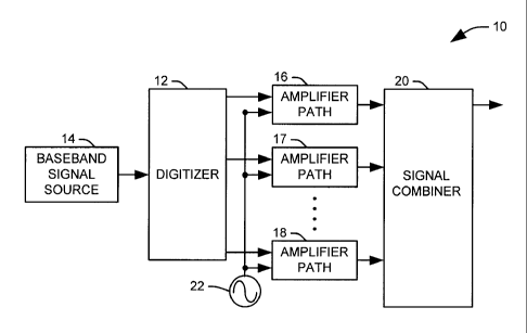
FIG. 1 is a functional block diagram of an amplifier
system 10 in accordance with an aspect of the present
invention. The system 10 includes a signal digitizer 12
configured to receive a baseband input signal from a
baseband signal source 14 and acquire samples of the
CA 02839213 2014-01-10
- 6 -
signal's amplitude with a given sampling frequency to
produce an N-bit digital signal representing a scaled
linear function of the amplitude of the baseband input
signal. In this context, N is an integer greater than
one. For example, the signal digitizer 12 can include
one or more analog to digital converter (ADC) assemblies
configured to provide the digital signal at a desired
sampling rate.
The signal digitizer 12 can further include a linear
transformer (not shown) implemented in a digital domain.
The transformer applies a linear function on the sampled
amplitude of the baseband input signal to accommodate a
particular amplitude modulation type, such as adding a DC
component and/or changing sign of the signal. It will
thus be appreciated that the digital signal can represent
any linear function of the baseband input signal having a
non-zero linear coefficient.
The system further includes N amplifier paths 16-18,
each associated with one bit of the digital signal
produced by the signal digitizer. In one implementation,
each amplifier path 16-18 includes a discrete RF phase
shifter, an RF switch and an amplifier path. Each
CA 02839213 2014-01-10
- 7 -
plurality of discrete phase shifters that can selectively
apply respective phase shift values to the RF carrier
signal delivered to its associated amplifier path
according to the values of the bits more significant than
the associated bit of the amplifier path. Accordingly,
in this implementation, the dedicated data bus broadcasts
the content of all significant bits in an N-bit binary
envelope sequence provided to each discrete phase
shifter.
Each RF switch is associated with a particular
amplifier path and receptive only to the bit from the N-
bit binary envelope sequence associated with its
amplifier path. Every time the associated bit assumes a
first value, the RF switch connects RF signal from an RF
signal source to the input of the associated amplifier
assembly. Every time the associated bit assumes a second
value, the RF switch disconnects the RF signal from an
input of the associated amplifier assembly and
effectively mutes the path.
The system further includes a plurality of amplifier
paths 16-18 that each receive a radio frequency (RF)
carrier signal from an associated RF carrier source 22,
CA 02839213 2014-01-10
- 8 -
for example, delivered through the associated discrete
value phase shifter and RF switch. It will be
appreciated that a given amplifier path 16-18 can include
multiple amplifier stages connected in series or in
parallel, connected via appropriate signal splitters and
combiners (not shown). The amplifiers associated with a
given amplifier path 16-18 can each include an active RE
power generating device, such as a bipolar junction
transistor (BJT), a metal-oxide semiconductor field
effect transistor (MOSFET), or an electronic tube.
Each of the amplifier paths 16-18 that are active at
a given time provide an RE output signal to a signal
combiner 20. The signal combiner 20 combines the outputs
of the plurality of amplifier paths 16-18 to deliver an
output signal having amplitude modulation that is
essentially a scaled replica of the binary envelope
sequence. In one implementation, the signal combiner
assembly 20 can include a series of hybrid combiners,
with the output of a first amplifier path 16 connected to
an isolation port of a first hybrid combiner, and two
outputs of a second amplifier path 17 connected to
corresponding through and coupled ports of the first
CA 02839213 2014-01-10
- 9 -
hybrid combiner. The output of the first hybrid combiner
can be connected to the isolation port of a next hybrid
combiner, with two outputs from a third amplifier path
connected to corresponding through and coupled ports of
the second hybrid combiner. This arrangement can be
continued until a final hybrid combiner that receives the
combined output signal of the previous amplifier paths at
an isolation port, and outputs from a final amplifier
path 18 at through and coupled ports. In one example,
illustrated in detail in FIGS. 2 and 3, each amplifier
path 17-18 after a first amplifier assembly 16 is
configured to provide RF signal with twice the voltage
level of the RF signal delivered by the previous
amplifier path. Accordingly, the output signal from the
signal combiner 20 can take on any of 2N voltage values
from the binary series
Votzt= 0,171,2171,3V1, ..,2N-1.171,.,(2N--1).Vi, where N is the
number of amplifier paths, equal to the dimension of the
binary envelope sequence, and V/ is the voltage of output
RF signal generated by the first amplifier path.
In accordance with an aspect of the present
invention, the operational status of each amplifier path
CA 02839213 2014-01-10
- 10 -
is controlled by the values in the N-bit binary sequence
distributed inside of the system by the signal digitizer
12. The operational status of the first amplifier
assembly is controlled by the value of a least
significant bit (LSB) in the binary sequence. The
operational status of the second amplifier assembly is
controlled by the value of the second least significant
bit in the binary sequence, and so on. Accordingly, in
the proceeding discussion, each amplifier path 16-18 can
be referenced by its assigned significant bit. For
example, the first amplifier path 16 can be referred to
as the LSB amplifier path and the last amplifier assembly
path can be referred to as the most significant bit (MSB)
amplifier path.
FIGS. 2 and 3 illustrates an example implementation
of a system for generating high power and high efficiency
amplitude modulated RF signals in accordance with an
aspect of the present invention. The illustrated system
can be utilized to provide amplitude modulated RF signals
over a wide range of operating RF frequencies. High
efficiency operation is achieved by employing RF power
transistors biased in Class C and driven into voltage
CA 02839213 2014-01-10
- 11 -
saturation mode when operational. A plurality of power
amplifiers are arranged in a series of amplifier
assemblies and used to amplify an RE' carrier signal, with
each power amplifier comprising RE' power transistors and
components arranged to form input and output matching
circuits. The output of each amplifier assembly is
coupled to one or more corresponding ports of an output
power combiner to construct an amplitude modulated output
signal.
FIG. 2 illustrates a front end 30 of the illustrated
system that provides both a carrier signal provided to
each of the plurality of amplifier paths and a digital
signal, based on the baseband signal amplitude, to
selectively activate the amplifier paths. An RE' carrier
source 32 receives a baseband input signal from a
baseband signal source 34 at a frequency upconverter 36,
where the signal is converted to a desired RE' frequency.
The RE' signal is then filtered at a bandpass filter (BPF)
38 around a desired carrier frequency to remove unwanted
modulation products and provided to an amplitude limiter
39 that attenuates the signal beyond a desired envelope
to remove any remaining amplitude modulation from the
CA 02839213 2014-01-10
- 12 -
signal. The resulting RF carrier signal is provided to
the back-end of FIG. 3, at point A.
A signal digitizer 40 samples the baseband input
signal at a selected sample rate at an analog-to-digital
converter and produces a binary envelope sequence of N-
bit digital words, each representing instantaneous
envelope of the RF signal, where N is an integer greater
than one. In the illustrated implementation, a sequence
of N-bit digital words is produced at an analog-to-
digital converter 42 and modified at a linear transform
44 to provide a binary envelope sequence representing a
linear function of the baseband signal amplitude. It
will be appreciated that this linear function can include
a linear coefficient applied to the offset, which can be
positive or negative, as well as an offset value,
depending on the application. In one implementation, the
linear coefficient is one and the offset is zero, such
that the digital signal represents the baseband signal
amplitude without modification. The resulting N-bit
digital signal is broadcast to the amplifier assemblies
via a dedicated data bus, represented in FIG. 2 as point
B.
CA 02839213 2014-01-10
- 13 -
The N-bit digital signal is also provided to a
linearity corrector 46 which ensures that the output of
the system is an accurate representation of the N-bit
digital signal. A sample of the output signal of the
amplifier system, represented by point C, is provided to
an RF demodulator 48 to downconvert a provided
representation of the system output to the baseband
frequency. The downconverted signal is provided to an
analog-to-digital converter 49 to produce a digital
representation of the downconverted signal. This digital
representation is compared to the N-bit digital signal at
a linearity corrector to ensure that the system output
has amplitude modulation that is an accurate replica of
the N-bit digital signal. Any non-linearity introduced
by the plurality of amplifier paths can be addressed by
altering the supply voltage provided to each path
according to this comparison.
FIG. 3 illustrates a back-end 50 of the example
system of FIGS. 2 and 3 comprising a plurality of
amplifier paths 52-56 and a power combiner 58 for
combining the outputs of the plurality of amplifier
paths. Each of the N amplifier paths 52-56 is provided
CA 02839213 2014-01-10
- 14 -
with each value of in the N-bit digital signal, provided
at the signal digitizer 40 of FIG. 2 and represented as
point A in FIG. 3, and is associated with a bit in the N-
bit digital signal. For example, a first amplifier path
52 can be associated with a least significant bit (LSB),
a second amplifier path 53 can be associate with a next
bit, and so on, with a most significant bit (MSB)
associated with an Nth amplifier path 56. The bit
associated with each amplifier path 52-56 is used to
control respective RF switches 60-64 in each amplifier
path. When the bit associated with a given amplifier
path 52-56 takes on a first value (e.g., a "1"), the
associated RF switch 60-64 is enabled to deliver an RF
signal to an input of an amplifier assembly 66-70
associated with the amplifier path. When the bit
associated with the amplifier path 52-56 takes on a
second value (e.g., a "0"), the RF switch 60-64 is not
enabled, and the amplifier assembly 66-70 is mute.
The input for each amplifier path 52-56 is supplied
as an RF carrier signal generated at the RF carrier
source 32 of FIG. 2, and represented by point B in FIG.
3. In the illustrated implementation, the RF carrier
CA 02839213 2014-01-10
- 15 -
signal can be delayed by various continuous phase
shifters 70-73 associated with the last N-1 amplifier
paths 53-56. The purpose of the continuous phase
shifters 70-73 is to provide appropriate phase delay
between consequent amplifier paths. The delay is needed
to account for propagation delays between the amplifier
paths 52-56. Introducing appropriate compensating delay
assists in providing phase conditions for the RF signals
generated by the amplifiers to combine in phase at the
output of each combining stage of the power combiner 58.
It will be appreciated that the phase delay provided by
the continuous phase shifters 70-73 can be adjusted to
allow the system to operate at different frequencies.
Each of the first N-1 amplifier paths 52-55 further
include a discrete RF phase shifter 74-77 to provide a
further delay to the RF carrier signal prior to
amplification. Each of the discrete RF phase shifters
74-77 are similar and serve to implement a phase shift to
a given RF signal within a given amplifier path 52-55 to
account for a discrete phase change of RF signal
reflected from the output of amplifier assemblies 67-70
CA 02839213 2014-01-10
- 16 -
located downstream in a combining path of the power
combiner 58.
The phase change occurs when these downstream
amplifier assemblies 67-70 change status from mute to
active and back to mute. Each downstream amplifier
assembly 67-70 is therefore characterized with a
corresponding phase change value. Each discrete phase
shifter can be programmed with a subset or all of the
discrete phase shift values associated with each
amplifier assembly, to implement a phase shift value yn
such that:
µPn, =
q.
Eq. 1
where N is the dimension of the binary word, n is a
sequential value of a significant bit associated with a
given amplifier path, Oi is a phase change value
associated with an ith amplifier assembly, And di is the
value of an ith bit within (1-1-1)iN range.
In other words, if a given bit 6i=1, the
corresponding phase shift is added to the sum. If the
bit 8i=0 the phase change is omitted from the sum.
Accordingly, the first phase shifter 74, associated with
CA 02839213 2014-01-10
- 17 -
the first amplifier path 52, can apply a combination of
(N-1) different phase shift values that belong to (N-1)
amplifier assemblies that follow the first one. The
phase shifter that belongs to the (N-1) st amplifier path
55 can have only one phase shift value
= 6",y (19 or- 1.) TIN , where ösy is the binary bit
value of the MSB. As will be appreciated, the MSB will
shift between zero and one during operation, affecting
the phase shift values inside previous (N-1) amplifier
paths. To facilitate this, the entire N-bit word
sequence can be provided via a dedicated bus to each of
the amplifier paths 52 and received by all phase shifters
at the same time.
In the illustrated implementation, the power
combiner 58 is formed from a plurality of hybrid
combiners connected in series, with the output of each
hybrid combiner coupled to an isolation port of a
subsequent hybrid combiner, and the output of a final
hybrid combiner in the series providing the output of the
system, indicated here as point C. In this
implementation, the first amplifier assembly 66 includes
a power amplifier that provides its output to the
CA 02839213 2014-01-10
- 18 -
isolation port of a first hybrid combiner of the series
of hybrid combiners comprising the power combiner 58.
The second amplifier assembly 67 includes two power
amplifiers that each provide their output to one of the
through and the coupled ports of the first hybrid
combiner.
The power amplifier associated with the first
amplifier assembly 66 is configured to provide a first
output voltage, 171, when operated in saturation. Each of
the two power amplifiers associated with the second
amplifier assembly 67 is configured to generate, when
operated at saturation, an output voltage equal to A571.
When the second amplifier assembly 67 is active, it
contributes an RF signal with amplitude 2V1 to the output
of the first hybrid combiner. Accordingly, a first
hybrid combiner within the power combiner 58 can deliver
one of four voltage levels (0, Vu 2V1, or 3V1), generated
by the either or both of first amplifier assembly 44 and
the second amplifier assembly. These voltage levels
represent the two least significant bits of the digitized
baseband input signal.
CA 02839213 2014-01-10
- 19 -
Every subsequent combining stage, represented by a
hybrid combiner and its associated amplifier assembly,
provides additional voltage levels. Specifically, an rth
hybrid combiner in the power combiner 58, in combination
with its associated (r+1) th amplifier assembly, provides
RF signal with an additional 2r equally spaced voltage
levels for the system output. For example, a system with
three RF amplifier paths and two combining stages
provides output RF signal with eight equally spaced
output voltage levels, with the first two amplifier paths
providing four output levels and combination of all three
amplifier paths providing additional four output levels.
A system with four amplifier assemblies and three
combining stages provides output RF signal with sixteen
output voltage levels, with the first two amplifier paths
providing four output levels, the third amplifier path in
combination with first two amplifier paths providing four
additional output levels, and a combination of all four
amplifier paths providing eight additional output levels.
All voltage levels are integer multiples of V1. Thus,
every new amplifier assembly represents an additional
binary bit.
CA 02839213 2014-01-10
- 20 -
To be able to follow the binary sequence and deliver
twice the voltage level of the previous stage, every
additional amplifier assembly should either contain four
times the number of RF power devices operating in
parallel employed at the previous path amplifier or have
a smaller number of correspondingly more powerful devices
operating in parallel. For example, if the power
amplifier in the first amplifier assembly contains one
transistor in the output stage, then each output power
amplifier in the second amplifier assembly should contain
two transistors operating in parallel, each output power
amplifier in the third amplifier assembly should contain
eight transistors operating in parallel, and each output
power amplifier in the fourth amplifier assembly should
contain thirty-two transistors operating in parallel.
The transistors can be connected in parallel using either
an in-phase or an out-of-phase combiner.
As discussed previously, each discrete phase shifter
74-77 is programmed to remember individual phase shift
values associated with each amplifier path 45,õ These
individual phase values are measured during each
amplifier path characterization process when the phase of
CA 02839213 2014-01-10
- 21 -
RF signal generated by the previous amplifier path
propagating down the combining path is reflected from
next amplifier assemblies output. The phase of the
reflected RF signal changes depending on operational
status of encountered amplifier assembly. The reflected
signal phase shift (ideally 1800) that happens when
amplifier is switching from mute mode to voltage
saturation mode is measured across operational frequency
range and stored in each discrete phase shifter. To
reflect this, the phase values are associated with
particular significant bits received by the phase
shifters through the dedicated data bus from the signal
digitizer 40 of FIG 2, as shown in Eq. 1, above. The
total phase shift is determined as a function of
modulation envelope amplitude and implemented for each
envelope value following the sampling sequence.
The discrete RF phase shifters 74-77 are operated
such that its corresponding output signal is amplified
and, after propagating through the plurality of output
combiners arrives to the system output in-phase with the
RF signals from the other amplifier paths. The
propagation path of the RF signal generated by each
CA 02839213 2014-01-10
- 22 -
amplifier assembly includes reflecting of the RF signal
from the output of the encountered amplifier assemblies,
and thus an active amplifier assembly representing a most
significant bit of the system output will have no phase
shift applied. The reflection phase depends on the
operational status of the encountered amplifier. Ideally
the signal reflected from the inactive or mute amplifier
output is out-of-phase with the signal reflected from the
saturated amplifier output. To account for this phase
change the signal generated by the previous significant
bit amplifier should be correspondingly pre-shifted
180 out-of-phase every time when the next higher
significant bit amplifier is operational. This would
provide a necessary condition for the signals generated
by both lower bit and higher bit amplifiers to propagate
in-phase to the system output. The real value of the
phase shift due to the difference in reflection angle
between mute and operational saturated amplifier output
is generally less than 1800. It is specific to the
parasitic parameters of RF power generating device,
output matching circuit and frequency of operation.
CA 02839213 2014-01-10
- 23 -
Correspondingly, the phase shift correction is less than
180 .
To better understand the use of the discrete phase
shifters 74-77 in providing efficient combination of the
amplifier assembly outputs, it is instructive to examine
the interaction of RE signal generated by the first
amplifier assembly 66 with the RE signal generated at the
output of the second amplifier assembly 67. If the first
amplifier assembly 66 is mute, the impedance Z20 is a
nominal load impedance at the outputs of the power
amplifiers in second amplifier assembly 67.
When driven with a sufficiently high input RE
signal, the active devices in the second amplifier
assembly 67 enter voltage saturation mode. The amplitude
of the output RE signal grows to a maximum value and
becomes limited by the power supply voltage. At that
moment, the amplitude of the output signal is no longer
increasing and the efficiency of the amplifiers
approaches its highest point. It will be appreciated
that device operation in or close to the voltage
saturation mode is most efficient.
CA 02839213 2014-01-10
- 24 -
An RF power device in voltage saturation mode is
approaching a voltage source and as such exhibits low
output impedance. Therefore, each amplifier in the
second amplifier assembly can be considered as RF voltage
source when the amplitude of the output signal of the RF
power amplifying devices situated inside of the power
amplifiers reaches the voltage limit determined by power
supply voltage.
A typical value of power MOSFET output impedance in
voltage saturated mode can be much lower than a typical
value of the load impedance presented at the output of
this device. Hence, devices operating in saturation mode
can be qualified as a fairly good voltage source. As
such, the device presents two important characteristics.
First, when the device is in voltage saturation mode, the
amplitude of the RF voltage at the output port of the
device is not particularly sensitive to the input RF
drive and is effectively determined by the power supply
voltage. Therefore, an amplitude of RF signal at the
output of each amplifier assembly can be tuned for a
specific value by setting up a corresponding DC power
supply voltage. These DC power supply voltages can be
CA 02839213 2014-01-10
- 25 -
continuously refined by the linearity corrector 46 of
FIG. 2 to maintain a linear operation of the system.
Further, an RF signal applied from an external power
source to the output port of the device will bounce back
due to the high reflection coefficient of the active
device output. The phase of the reflected signal depends
on whether the amplifier is mute or driven into
saturation.
The latter characteristic provides an opportunity
for the RF signal generated by first amplifier assembly
66 to combine in-phase with the signal generated by the
second amplifier assembly 67 at the output port of the
first hybrid combiner and, simultaneously, to reduce load
impedance at the active device output of the second
amplifier assembly when both amplifiers are operational.
For this, the phase of the signal supplied by the first
amplifier assembly 66 should be shifted so that the first
signal would arrive at the outputs of the active devices
included in the output stage of the second amplifier
assembly 67 out-of-phase with the signal generated by the
second amplifier.
CA 02839213 2014-01-10
- 26 -
Ideally the phase step applied to the first RF
signal, when both first and second paths 52 and 53 are
operational, would be 1800. This phase step corresponds
to the difference incurred when the same RF signal
generated by a finite impedance source is being reflected
from a current source (mute mode) as opposed to a voltage
source (saturation mode). The corresponding phase
difference between two reflected RF signals would be
180 . Therefore, if we want the reflected signals in
both cases have the same phase we need to change phase of
one of the incident signals 180 . In reality, the output
of the active device in cut-off mode is far from being a
current source. It has a strong reactive component due
to inherent parasitic capacitance. As result, the phase
of the RF signal reflected from the muted active device
in cut-off mode can be significantly different from 0 .
This makes the difference between phases of the RF signal
reflected from the second amplifier output when it is in
mute mode as opposed to saturated mode less than 180 .
We introduced an arbitrary phase step 9 (0 9 ._. 180 )
that is device specific. The phase step is applied to
the first RF signal when both first and second amplifiers
CA 02839213 2014-01-10
- 27 -
are operational. This creates conditions for both RE'
signals to combine in phase at the system output.
As a result of applying the phase shift, the load
impedance presented at the output port of the active
devices of the second amplifier assembly 67 is reduced,
which allows the power of the RE' signal generated by the
second amplifier output stage to grow higher while the
output stage remains in voltage saturation mode. This is
accomplished by constructing each amplifier path with
amplifier driver stages having some extra gain and extra
power level capability. This way the RE' signal level
generated by the driver stage is high enough for the
output amplifier stage to remain in voltage saturation
mode when the load impedance drops. The level of RE'
voltage at the output port of each active device inside
the output stage of second amplifier assembly 67 is not
changing during this exercise. As a result, the output
power level generated by this amplifier path 53 grows
inversely proportional to the load impedance change.
To achieve this load pulling effect, the RE' signal from
the output of first amplifier assembly 66 is applied to
CA 02839213 2014-01-10
- 28 -
the isolation port of the first hybrid combiner of the
power combiner 58.
Following the properties of a two-way 3dB ninety-
degree hybrid splitter, the signal propagates to the
outputs of amplifiers of the second amplifier assembly
43, splitting equally between them. Each signal travels
further to the output port of active devices, and, in the
illustrated implementation, the devices are biased in
Class C and, therefore, have a high output reflection
coefficient. Both amplifiers are identical and therefore
have identical reflection coefficients. Both RF signals
reflect back and arrive at the corresponding input ports
of the output hybrid combiner with their phases shifted
ninety degrees relative to each other. Given the
properties of a three decibel, ninety-degree hybrid
combiner, both signals will travel to the output port of
the hybrid combiner and recombine there. Given a high
directivity of the hybrid combiner, negligibly low level
reflection signal is delivered back to the output of the
first amplifier assembly 66. By propagating to the
output ports of the active devices within each power
amplifier the load impedance presented at the ports is
CA 02839213 2014-01-10
- 29 -
changed. The direction of the change is determined by
the phase relationship between two interacting RF signals
at the AD output port. If the signals are out-of-phase,
and the discrete phase shifter 74 associated with the
first amplifier path 54 can be controlled to ensure that
they are, the impedance drops. Accordingly, the output
power delivered by the second amplifier assembly 67 grows
inversely proportional to the impedance drop.
FIG. 4 is a chart 80 illustrating the effects of the
first amplifier RF output voltage, VI, on the load
impedance, Z2, presented at the output port of the active
devices of the second amplifier assembly 67. A vertical
axis 72 represents the ratio of Z2 to the nominal load
impedance, Z20. A horizontal axis 74 represents the
ratio of the output voltage, VI, of the first amplifier
assembly 66 to a saturation voltage, V2sat, of the power
amplifiers of the second amplifier assembly 67. Positive
values on the horizontal axis indicate that the output
signal of the first amplifier assembly 66 is delivered in
phase with the output signal of the second amplifier
assembly 67 at the output ports of the active devices in
the second amplifier assembly, while negative values
CA 02839213 2014-01-10
- 30 -
indicate that the two signals are out-of-phase. The
relationship between the two for the system of FIG. 2 is
plotted as a solid line 76.
In general, the load impedance, Z2_sat, presented at
the active device output port when operating at
saturation can be expressed as a function of an RE' signal
voltage generated by the first amplifier assembly, 1/17, and
a saturation voltage, V25at, of the second amplifier
assembly as:
Z20
Z2 _ sat =
V Eq. 2
1-N/2 ___________________ I
V2sal
As can be seen from the chart, the load impedance at
the output of the active devices can be reduced to
approximately half the nominal value when 1/1 is equal to
(-V2 sat i'j) =
It will be appreciated that the phase shift applied
to the carrier signal provided to the first amplifier
assembly 66 and the second amplifier assembly 67 can be
selected such that the signals generated by the two
amplifier assemblies arrive out-of-phase with the signal
generated by third amplifier assembly 44 at the output
ports of the active devices within the third amplifier
CA 02839213 2014-01-10
- 31 -
assembly. This can be continued for each of the N
amplifier assemblies 66-70, such that an output RF signal
having envelope representing the transformed amplitude of
baseband input signal can be achieved.
FIG. 5 illustrates a detailed view 100 of the
amplifier assemblies 102-104 and a signal combiner 106,
of an example implementation of a system in accordance
with an aspect of the present invention. In the
illustrated implementation, three amplifier assemblies
102-104 are used to provide a simplified example,
although it will be appreciated that systems and methods
in accordance with an aspect of the present invention can
be expanded to more than three amplifier assemblies.
In the illustrated implementation, five power
amplifiers 108-112 are employed to provide three
amplifier assemblies, including an amplifier 108
associated with a first amplifier assembly 102, two
amplifiers 109 and 110 associated with a second amplifier
assembly 103, and two amplifiers 111 and 112 associated
with a third amplifier assembly 104. It will be
appreciated that the amplifiers 108-112 can include any
appropriate assemblies for high power amplification of RE
CA 02839213 2014-01-10
- 32 -
signals. For example, each amplifier 108-112 can contain
one or more active devices operating in parallel, a
direct current (DC) power supply for the active devices,
and appropriate impedance matching circuitry at the input
and output of the device. The active devices can be
implemented to include, for example, metal-oxide
semiconductor field effect transistors (MOSFETs), bipolar
junction transistors (BJTs), junction gate field effect
transistors (JFETs), or vacuum tubes. In the illustrated
implementation, each of the amplifiers 85-89 is biased in
class C.
FIG. 6 illustrates one example of an amplifier 130
that can be used in a system in accordance with an aspect
of the present invention. The amplifier 130 includes an
input impedance matching component network 132, an active
device 134, a direct current (DC) power supply and bias
circuit 136, and an output impedance matching network
138. While the amplifier 130 is shown with one active
device 134, it will be appreciated that an amplifier in
accordance with an aspect of the present invention can
include multiple active devices operating in parallel.
For example, the amplifier could include two devices in
CA 02839213 2014-01-10
- 33 -
push-pull configuration or a number of devices connected
in parallel with an in-phase combining network. In the
illustrated implementation, the active device 134 is
implemented with a MOSFET 142. It will be appreciated,
however, that the active device 134 could include one or
more of a bipolar junction transistor (BJT), junction
gate field-effect transistor (JFET), a vacuum tube, or a
similar device. Depending on a particular kind of active
device employed, a corresponding quiescent bias feed can
be provided.
It will be appreciated that, throughout this
document, any discussion of the impedance within an
amplifier assembly refers to the impedance at the output
of the active device of a given amplifier of the
amplifier assembly. So, this is intended to refer to a
point 144.
Returning to FIG. 5, each amplifier assembly 102-104
is provided with an RF carrier signal for amplification.
The RF carrier signal is amplified at the first amplifier
108 to provide a first amplified signal, representing the
first amplifier assembly 102. The second amplifier
assembly 103 includes a first three-decibel, ninety-
CA 02839213 2014-01-10
- 34 -
degree signal splitter 114 that distributes the RF
carrier signal equally between the two identical output
stage amplifiers 109 and 110 associated with the second
amplifier assembly 103. Each of the output stage
amplifiers 109 and 110 provide a second amplified signal
to one of the through and coupled ports of a first three-
decibel, ninety-degree hybrid combiner 116. The first
amplified signal, from the first amplifier assembly 108,
is delivered to an isolation port of the first hybrid
combiner 116.
The third amplifier assembly 104 includes a second
three-decibel, ninety-degree signal splitter 118 that
distributes the RF carrier signal equally between the two
identical output stage amplifiers 111 and 112 associated
with the third amplifier assembly 104. Each of the two
amplifiers 111 and 112 comprising the third amplifier
assembly 104 delivers a third amplified signal to a
second three-decibel, ninety-degree hybrid combiner 120.
The output of the first hybrid combiner 116 is connected
to an isolation port of the second hybrid combiner 120.
The resulting output of the second hybrid combiner 120
represents the output of the amplifier system.
CA 02839213 2014-01-10
- 35 -
FIG. 6 illustrates a method 200 for generating a
modulated radio frequency (RF) output signal representing
a baseband input signal. At 202, a sample of the
baseband input signal is digitized to provide an N-bit
digital signal representing the input signal, where N is
an integer greater than one. At 204, the input signal is
transformed according to a predetermined linear function.
It will be appreciated that the linear transform can be
represented as a positive or negative scaling multiplier
and a positive or negative offset value. In one
implementation, the multiplier is one and the offset is
zero, such that the resulting digital signal forms a
direct proportion between the input baseband signal
amplitude and output RF signal envelope.
At 206, an RF carrier signal is formed by up-
converting the input baseband signal and eliminating the
amplitude modulation by using amplitude hard limiter.
At 208, the RF carrier signal is provided to each of N
amplifier assemblies. In one implementation, (N-1)
summary status values Szwqon are also derived from the
baseband input signal, representing phase shifts to be
applied to the inputs of at least some of the N amplifier
CA 02839213 2014-01-10
- 36 -
assemblies. Accordingly, a phase shift can be
selectively applied to the RF carrier signal supplied to
at least a subset of the N amplifier assemblies according
to the value of Sz(nywn, such that a given amplifier
assembly in the subset receives the RF carrier signal
with a predetermined phase shift when its associated bit
assumes a first value and without the predetermined phase
shift when its associated bit assumes a second value.
At 210, each of the N amplifier assemblies are
operated according to the value of an associated
significant bit within the N-bit word, such that a given
amplifier assembly is active when its associated bit
assumes a first value and mute when its associated bit
assumes a second value. Amplitudes of RF signals
generated by different amplifier paths can differ from
each other, such that the combined output of the N
amplifier assemblies has an applied amplitude modulation
representing the transformed digitized baseband input
signal. For example, each assembly can have a operating
output voltage of generated RF signal twice that of a
preceding amplifier assembly. At 212, the output signals
of the N amplifier assemblies are combined to provide the
CA 02839213 2014-01-10
- 37 -
output RF output signal. For example, the output signals
of the N amplifier assemblies can be delivered to a
series of hybrid combiners in which an output port of
each hybrid combiner in the series, other than a final
hybrid combiner in the series, is connected to an
isolation port of a subsequent hybrid combiner in the
series. The output of the final hybrid combiner in the
series provides the system output.
The systems and methods described in FIGS. 1-6
provide a number of advantages. RF communication signals
created with digital modulation techniques can be
characterized by a Peak-to-Average Power Ratio (PAPR).
The high definition television broadcast industry employs
such modulation standards, for example, in the Very High
Frequency (VHF) and Ultra High Frequency (UHF) bands.
One example would be the Digital Video Broadcasting -
Terrestrial (DVB-T) modulation used in many countries
around the world. A single TV channel can include many
spectral carriers (e.g., thousands) tightly spaced over
an 8MHz frequency range. This creates a signal with
amplitude modulated envelope varying between zero
CA 02839213 2014-01-10
- 38 -
amplitude and amplitude of 6db to 12dB above average
signal level depending on the modulation standard used.
Currently used Class AB RE' amplifiers operate at
average power levels backed off from their peak power
capability by the factor of PAPR. This leads to a
relatively low DC-RE' efficiency. A system in accordance
with the present invention allows for the use of power
amplifiers biased in class C and operating at or near
saturation much of the time, greatly increasing the
efficiency of the system.
In addition, the systems and methods described
herein are not frequency sensitive. Most countries have
their frequency range allocated for television (TV)
channels that spans from 470MHz to 862MHz at UHF and from
175MHz to 252MHz at VHF. The TV allocated frequency span
at UHF is 59% wide and at VHF is 36% wide. Many
broadcasting networks prefer to have transmitters that
can operate at any channel within UHF or VHF frequency
range without physical adjustments.
A system in accordance with the present invention
provides such possibility by incorporating a lossless
load pulling at the active device output to the frequency
CA 02839213 2014-01-10
- 39 -
range boundaries of a three-decibel hybrid combiner.
This is done by introducing a novel output power
combining technique. As a result, a high efficiency,
high power amplitude modulator can operate across a
frequency range as wide as the bandwidth of 3dB hybrid
combiner. The operating bandwidth of three decibel
hybrid combiners can be extended by adding quarter
wavelength sections to the construction of the combiner
and properly organizing the corresponding coupling levels
between transmission lines.
From the above description of the invention, those
skilled in the art will perceive improvements, changes,
and modifications. Such improvements, changes, and
modifications within the skill of the art are intended to
be covered by the appended claims.