Note: Descriptions are shown in the official language in which they were submitted.
CA 02839780 2013-12-17
rise2tC,--e
Pr rl
PET I SE 2n11.: ; 0 5 0 8 9 1
2 4 -04- 2013
METHOD FOR PRODUCING A NEUTRON DETECTOR COMPONENT, A
NEUTRON DETECTOR COMPONENT, USE THEREOF FOR DETECTING
NEUTRONS AND A NEUTRON DETECTING DEVICE COMPRISING
NEUTRON DETECTOR COMPONENTS
Technical field
The present disclosure relates to a method for producing a neutron
detector component comprising a neutron detecting boron carbide layer
comprising boron-10 arranged on a substantially neutron transparent
substrate. The disclosure also relates to a neutron detector component for
use in a neutron detector, the use of such a neutron detector component for
neutron detection, and a neutron detecting device comprising a plurality of
neutron detector components arranged as a stack.
Technical background
Due to the approaching very limited availability of 3He and unaffordable
prices of the same, new kinds of neutron detectors not based on 3He, are
urgently needed, especially for large area neutron detector applications. One
possible replacement for 3He for neutron detection is the boron isotope 1 B.
1013 has a relatively high neutron absorption cross section, resulting in an
absorption efficiency of 70% compared to 3He, at a neutron wavelength of
1.8 A. Naturally occurring boron contains 20% of 106, but due to the almost
10% mass difference to the other boron isotope, 11B, the isotope separation is
relatively simple.
Use of 10B in neutron detectors is known both in the scintillator, the
gas, and the conversion layer varieties.
In US 6,771,730 a semiconductor neutron detector is shown having a
boron carbide (B4C) semiconducting layer, the B4C layer containing 10B. The
10134C layer was deposited on doped silicon using plasma-enhanced chemical
vapor deposition (PECVD). Synthesis of semiconducting 64C may not be
possible using other methods.
AMENDED SHEET
CA 02839780 2013-12-17
rhe Swe- = =Cc
PCT = KT SE nvi 1 0 5 0 8 9 1
24 -04- 2013
2
However, CVD techniques are in general, due to the use of gaseous
materials, associated with process risks and also high material costs.
Summary of the invention
Although the theoretical neutron detection efficiency would be higher
with pure boron layers comprising boron-10 (1013), layers of boron carbide
comprising boron-10 are preferred for stability reasons, both from a
mechanical and contamination point of view. Physical vapor deposition (PVD)
is associated with less process risk and lower material costs than CVD.
However, when attempting to use PVD for producing layers of boron carbide
comprising boron-10, other problems arise. For example, when a neutron
detecting boron carbide layer comprising boron-10 is provided by direct use of
conventional PVD, adhesion to the underlying substrate typically become
lower than desirable, causing the layer to spall off or hindering formation of
a
continuous film. This may become a problem in particular for layer
thicknesses in the micrometer range, which thicknesses typically are
desirable to be able reach for neutron detection ability reasons, and when
temperature sensitive substrates are used, such as of aluminum, which often
is a material desirable to use as substrate.
Hence, in view of the above, one object of this disclosure is to
overcome or at least alleviate problems in the prior art, or to at least
present
an alternative solution. A specific object is to present a method for
producing
neutron detector components based on PVD, where the neutron detector
comprises a neutron detecting boron carbide layer comprising boron-10
arranged on a substantially neutron transparent substrate. Further objects are
to present a neutron detector component for use in a neutron detector, use of
such a neutron detector component for neutron detection and a neutron
detecting device comprising a plurality of neutron detector components
arranged as a stack.
The invention is defined by the appended independent claims.
Preferred embodiments are set forth in the dependent claims and in the
, following description and drawings.
According to a first aspect of the present invention, these and other
AMENDED SHEE I
CA 02839780 2013-12-17
I il'e = Cffice
r.tCfl PCT! SE
2011 / 0 5 0 8 9 1
2 4 -04- 2013
3
objects are achieved through a method for producing a neutron detector
component comprising a neutron detecting boron carbide layer comprising
boron-10 arranged on a substantially neutron transparent substrate, the
method comprising: placing the substantially neutron transparent substrate
substantially neutron transparent substrate by means of physical vapor
deposition in the form of magnetron sputtering using the at least one source
of coating material when said pressure and said elevated temperature are
reached, and coating the neutron detecting boron carbide layer comprising
By substantially neutron transparent substrate" is here meant a
substrate that is made of such material and has such thickness that the
It is implied that any heating of the substantially neutron transparent
It should be noted that presentational order of the steps of the method
should as such not be construed as limiting. Steps that are independent of
each other may be performed in different order and/or may be partly or wholly
AMENDED SHEE1
CA 02839780 2013-12-17
11 f2, ..tc7 Cfrice _____________________ 1 PCT SE
r". 1 0 5 0 8 9 1
PCT trnco-r, = - :;p:,cation
2 4 -04- 2013
4
As confirmed by experiments, the method enables improved adhesion
of the boron carbide layer to the substantially neutron transparent substrate,
thereby, in practice, allowing PVD to be used to provide boron-10 based
neutron detecting layers in the micrometer range and on aluminum
substrates. Although there is no wish to be bound by a particular explanation
of underlying reasons, it is believed that one reason for poor adhesion is
presence of contaminants in the boron carbide layer and on the substrate
surface, which to a great extent are removed by the method. Additionally,
there is increased risk for the boron carbide layer to spall off from the
substrate with increasing stresses in the coating. The present method
enables use of lower temperatures during coating, compared to conventional
methods, which reduces such stresses in the boron carbide layer. Moreover,
presence of contaminants in the boron carbide layer is also related to a
lowered neutron detection efficiency of the boron carbide layer. A further
advantage of the method is therefore also that it enables improved neutron
detection efficiency.
The method may further comprise heating of at least a coating surface
of the substantially neutron transparent substrate during the coating of the
neutron detecting boron carbide layer.
The heating of at least a coating surface of the substantially neutron
transparent substrate during the coating of the neutron detecting boron
carbide layer may comprise heating to at least said elevated temperature.
The heating of at least a coating surface of the substantially neutron
transparent substrate may comprise specific heating thereof.
By "specific heating" of at least a coating surface of the substantially
neutron transparent substrate is here meant that heating is specifically
directed for heating the substrate and not only what happen to result from the
PVD process as such. The specific heating may e.g. be accomplished
through direct heating of the substrate by e.g. supplying high electric
current
through the substrate, by indirect heating through e.g. radiation from a
heating element specifically arranged to heat the substrate, and/or by heating
of the substrate through utilization of energized species.
AMENDED SHEEI
CA 02839780 2013-12-17
_________________________________________________________________ PCT! SE
"L:1- 1 0 5 0 8 9 1
24 -04- 2013
The substantially neutron transparent substrate may be a temperature
sensitive substrate having a melting temperature that is at most about 660 C.
The method may further comprise: removing contaminants from the
coating chamber with the substantially neutron transparent substrate and the
5 source of coating material placed inside, prior to and/or during the
evacuating
of the coating chamber.
By "contaminant" is here generally meant any substance that is
undesirably present or present at an undesirable amount in the coating
chamber and that, if present during production, would have a detrimental
effect on the resulting product. Contaminants typically involve the elements
H,
C, N, 0, Ar, Ne or Kr, and compounds comprised of these elements, for
example H20, OH, 02, H2, CH4, N2, CO2, which typically occur bound to the
walls of the coating chamber and/or to the substrate and/or are present at or
in the source of coating material and/or are present in gases used in the PVD
process.
By "removing contaminants from the coating chamber" is meant to
include removal of contaminants that may be present anywhere inside the
chamber, including contaminants bound to the walls of the coating chamber,
and/or contaminants present at/in the source of coating material, and/or
contaminants bound to or present at/in the substantially neutron transparent
substrate.
The step of removing contaminants from the coating chamber may
comprise heating and degassing of the coating chamber, while keeping the
temperature of the substantially neutron transparent substrate below its
melting temperature.
The removing of contaminants from the coating chamber may be
performed during the evacuating of the coating chamber.
The heating of the coating chamber may comprise using heat from the
heating of at least a coating surface of the substantially neutron transparent
substrate.
The heating of the coating chamber may comprise using another
separate source of heat than is used for the heating of at least a coating
surface of the substantially neutron transparent substrate.
AMENDED SHEE1
CA 02839780 2013-12-17
c Fcs,e7
PCT SE 21 I 0 5 0 8 9 1
24 -04- 2013
6
The heating of the coating chamber may comprise heating thereof to at
least 100 C, or at least 200 C, or at least 300 C, or at least 400 C, or at
least
500 C, or at least 600 C.
The removing of contaminants from the coating chamber may include
removal of H20 contaminants.
H20 contaminants may be removed using a method directed
specifically at reducing H20 contaminants and may be selected from the
group consisting of electron beam, infrared radiation, ultraviolet light and
visible light irradiation, ion irradiation, contact with a resistive heating
element,
or a combination of any of these methods.
The temperature of at least a coating surface of the substantially
neutron transparent substrate may vary during the coating process, preferably
above the elevated temperature, but lower temperatures may be allowed as
well. However, the temperature of the substrate should not be significantly
below the elevated temperature and/or preferably only below the elevated
temperature during a minor part of the coating process.
Coating at higher temperatures, preferably as high as possible below
the melting temperature of the substrate, may result in better adhesion of the
neutron detecting boron carbide layer to the substantially neutron transparent
substrate and further reduce the amount of contaminants in the layer.
The pressure may be at most 3 mPa, preferably at most 1.5 mPa, or
more preferably at most 0.75 mPa.
The method may comprise coating of the substantially neutron
transparent substrate on opposing coating surfaces.
Although two-sided coatings may be desirable and advantageous for
many applications, coating may be performed on only one surface as well.
The substantially neutron transparent substrate may be electrically
conducting.
In the nuclear reaction between incident neutrons and 10E1 in the
neutron detecting boron carbide layer: 10E1+ n --+ 7Li + 4He + 2.3 MeV, the
'Li
and 4He isotopes leave the neutron detecting layer and may be detected with
both temporal and spatial resolution in a detecting gas. Upon leaving, the
neutron detecting layer is left with a negative net charge which may be
AMENDED SHEET
CA 02839780 2013-12-17
fte Swec.:i = Cf`Int".. 1
POT II n = PCT! SE 05089 1
2 4 -04- 2013
7
compensated for by conducting away electrons from the boron carbide layer
through the electrically conducting substantially neutron transparent
substrate.
The substantially neutron transparent substrate may comprise
aluminum or aluminum alloys. Such an alloy is for example a Si-Al alloy.
The neutron detecting boron carbide layer may be electrically
conducting.
The conductivity of the neutron detecting boron carbide layer should be
sufficient for neutralizing the negative net charge in the boron carbide layer
formed as a consequence of charged particles leaving the surface of the
neutron detecting layer upon the reaction between neutrons and 10B.
The desired thickness of the neutron detecting boron carbide layer may
be less than about 4 pm, or, less than about 3 pm, or, less than about 2 pm,
or, less than about 1.5 pm, or, less than about 1.3 pm, or, less than about
1.2
pm, or, less than about 1.1 pm.
The desired thickness of the neutron detecting boron carbide layer may
be at least about 0.2 pm, or, at least about 0.4 pm, or, at least about 0.6
pm,
or, at least about 0.8 pm or, at least about 0.9 pm, or at least about 1 pm.
The desired thickness of the neutron detecting boron carbide layer may
be in a range of about 0.3 pm to about 1.8 pm, preferably in a range of about
0.5 pm to about 1.6 pm, more preferably in a rage of about 0.7 pm to about
1.3 pm, and most preferably in a range of about 0.9 pm to about 1.1 pm.
The neutron detecting boron carbide layer may be coated directly onto
the coating surface of the substantially neutron transparent substrate.
The neutron detecting boron carbide layer may be coated onto an
intermediate or gradient layer, such as an adhesion-promoting layer.
There may be one or more intermediate or gradient layers between the
neutron detecting boron carbide layer and the substantially neutron
transparent substrate. By use of an intermediate or gradient layer further
improved adhesion may be possible.
The neutron detecting boron carbide layer may be a B4C-layer.
B4C-coatings can be made wear resistant with thermal and chemical
stability. B4C is here meant crystalline or amorphous compounds, or a
AMENDED MEV
CA 02839780 2013-12-17
I ri's E.%^.,e=-= ,; =IPert Offce KT SE r.-
÷t050891
PCJ ,)p;eation
24-04- 2013
8
combination thereof, consisting of B and C, where the B-content ranges
between about 70% and 84% of the total number of B and C atoms, i.e.
disregarding possible impurities. A lower carbon content would result in lower
long-term stability of the coating, since a B-rich coating is more reactive.
The
higher the carbon content of the boron carbide coating comprising boron-10,
the lower the neutron detection efficiency of the coating. By "detection
efficiency" is here meant the number of detected neutrons in relation to how
many neutrons that enter the neutron detecting boron carbide layer.
The at least one source of coating material may comprise boron-10
enriched 134C (10B4C).
The at least one source of coating material may preferably
substantially consist of boron-10 enriched B4C (10B4C). Normally B is a
mixture of 20% 1013 and 80% "B. Enriched 10B4C has in practice typically a
10B content of about 70 at.% to about 84 at.%. Instead of using 10B4C as a
single source of coating material, separate sources of 10B and C may be used
during the coating.
A neutron detector
component may be provided, that may be produced according to the method
described above, for use in a neutron detector, the neutron detector
component (1) comprising a neutron detecting boron carbide layer comprising
boron-10 arranged on a substantially neutron transparent substrate, wherein
the substantially neutron transparent substrate is a temperature sensitive
substrate having a melting temperature that is at most about 660 C.
The substantially neutron transparent substrate may be electrically
conducting.
The substantially neutron transparent substrate may comprise
aluminum or aluminum alloys.
The neutron detecting boron carbide layer may be electrically
conducting.
The neutron detecting boron carbide layer may have a thickness that is
less than about 4 pm, or, less than about 3 pm, or, less than about 2 pm, or,
less than about 1.5 pm, or, less than about 1.3 pm, or, less than about 1.2
pm, or, less than about 1.1 pm.
AMENDED SHEET
CA 02839780 2013-12-17
1 frf.E= N.PIC 'ert Office_
- "'l PCT I SE
7"! ' 0 5 0 8 9 1
24 -04- 2013
9
The neutron detecting boron carbide layer may have a thickness that is
at least about 0.2 pm, or, at least about 0.4 pm, or, at least about 0.6 pm,
or,
at least about 0.8 pm or, at least about 0.9 pm, or at least about 1 pm.
The neutron detecting boron carbide layer may have a thickness that is
in a range of about 0.3 pm to about 1.8 pm, preferably in a range of about 0.5
pm to about 1.6 pm, more preferably in a rage of about 0.7 pm to about 1.3
pm, and most preferably in a range of about 0.9 pm to about 1.1 pm.
The neutron detecting boron carbide layer may be coated directly onto
the coating surface of the substantially neutron transparent substrate.
The neutron detecting boron carbide layer may be a B4C-layer.
The boron-10 content of the neutron detecting boron carbide layer may
be at least about 65 at.%, preferably at least about 70 at.%, more preferably
at least about 75 at %, and most preferably in the range of about 80 to about
100 at.%.
According to a second aspect there is provided a use of the neutron
detector component described above for detecting neutrons.
According to a third aspect there is provided a neutron detecting
device comprising a plurality of neutron detector components arranged as a
stack.
The number of neutron detector components in the stack may be at
least 2, preferably at least 10, more preferably at least 15, even more
preferably at least 20, and most preferably at least 25.
The more neutron detector components used, thus resulting in more
neutron detecting layers, the more efficient neutron detection efficiency of
the
neutron detecting device. However, in practice the gain of more components
may at some point be so small that it does not motivate the increased cost
and complexity resulting from further components.
The detection efficiency of the neutron detecting device is at least
30%, preferably at least 40%, more preferably at least 50%, even more
preferably at least 60%, and most preferably at least 70%.
AMENDED SHErf
CA 02839780 2013-12-17
C=Ccc
PCT. c..aticn
PCT I SE 2G11 I 0 5 0 8 9 1
2 4 -04- 2013
Brief description of the drawings
The above, as well as other aspects, components and advantages of
the present invention, will be better understood through the following
illustrative and non-limited detailed description, with reference to the
5 appended drawings.
Fig. 1 schematically shows a cross-sectional view of a neutron detector
component according to a first embodiment.
Fig. 2 is a flow chart illustrating a method for producing a neutron
detector component.
10 Fig. 3 schematically shows a substrate in a growth chamber, the
substrate being specifically heated during production of the neutron detector
component.
Fig. 4 shows a neutron detecting device with N number of detector
components arranged as a stack.
In the drawings the same reference numerals may be used for same,
similar or corresponding features, even when the reference numerals refer to
features in different embodiments.
Detailed description
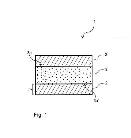
Fig.1 schematically shows a cross-sectional view of a neutron detector
component 1 having as neutron detecting layers a respective boron carbide
layer 2 comprising boron-10 (10B) of thickness t arranged on each one of
opposing coating surfaces 3a, 3a" of a substantially neutron transparent
substrate 3 that in one embodiment is made of aluminum. In other
embodiments the neutron detecting boron carbide layer 2 may constitute only
a sub-layer or sub-portion of a larger neutron detecting layer or neutron
detecting stack of layers, for example one layer in a multi-layered neutron
detecting stack. In some applications, such as for use in neutron detectors of
e.g. multi-grid type, a two-sided coating of the shown type is an advantage.
However, for other applications a one-sided coated substrate 3 may be
desirable and thus in other embodiments there may be a neutron detecting
layer 2 on only one side of the substrate 3. The neutron detector component
may have different shapes, which typically is determined by the design of the
A ARryktriZn SHEET
CA 02839780 2013-12-17
fl-Zi*.= pnt Cfce
' õõ , õ POT inieme Appk,ation
3C 4.;;:; 3
u 0 8 9 1
24 -04- 2013
11
neutron detector which the neutron detecting component 1 is to be used with.
However, typically the component is sheet-shaped or in the form of a neutron
detector plate or blade that may have a flat structure but may in other
embodiments be curved. The component may also e.g. be of tubular shape or
in the form of a wire.
The neutron detecting boron carbide layer 2 may, as in the shown
embodiment of fig. 1, be arranged directly onto the substantially neutron
transparent substrate 3. In other embodiments there may be one or many
intermediate or gradient layers, such as a layer to promote adhesion between
the substantially neutron transparent substrate 3 and the neutron detecting
boron carbide layer 2. Such an adhesive layer may for example be a layer
created in-situ by deposition from the same or a separate deposition
source(s) as the neutron detecting boron carbide layer 2. Such an adhesion
layer may be metallic or ceramic and have any chemical composition,
including that of the substrate 3, the neutron detecting boron carbide layer
2,
or of any other material of a larger neutron detecting layer comprising the
neutron detecting boron carbide layer 2 as a sub-layer or sub-portion. The
adhesion layer may also be created by in-situ surface modification induced by
ion irradiation, electron irradiation, photon irradiation, or a combination
thereof.
The thickness ,t, of the boron carbide layer 2 as neutron detecting layer
is generally typically above 0.2 pm and below 4 pm, or below 3 pm, or below
2.5 pm, or below 2 pm, or below 1.5 pm, or below 1 pm. In one embodiment it
is preferably in the range of 1 pm and 2 pm.
In the following an embodiment of a method for producing a neutron
detector component 1 will be discussed with reference to a detailed
embodiment, where the major steps of the method are shown in the flow chart
in fig.2.
In a first step 110, the substantially neutron transparent substrate 3 is
provided. In the detailed embodiment a 0.5 mm thick rolled aluminum (Al)
blade from the alloy EN AW-5083 is used as the substantially neutron
transparent substrate 3. In another embodiment an aluminum foil with a
thickness below 0.1 mm may be used as the substantially neutron transparent
AMEND'ED SHEE
CA 02839780 2013-12-17
Er.r CF.C.:1 1
..'eC 1
PCT SE 2.1,':1 0 5 0 8 9 1
2 4 -04- 2013
12
substrate 3. In yet other embodiments, substrates 3 having thicknesses up to
several millimeters may be used. In the detailed embodiment, the Al blade is
cleaned in ultrasonic baths of Neutracon followed by de-ionized water and
subsequently blown dry in dry N2. In other embodiments, the substrate 3 may
be cleaned by other means, including for example de-greasing in organic
solvents and/or etching in an acid.
In a step 120 the substantially neutron transparent substrate 3 and
source(s) of coating material 16 is placed inside a coating chamber of a
deposition system, for example a coating chamber 10 as schematically
illustrated in fig. 3. In the detailed embodiment, up to 24 Al blades (20 x
180
mm in size) are used as substrates 3 and mounted onto a sample carousel,
which allows for 2-axis planetary rotation and 2-sided depositions, and placed
in the coating chamber of an industrial CC800/9 deposition system
(CemeCon AG, Germany).
In a step 146 the coating chamber 10 is being evacuated to a pressure
that is at most 6 mPa and in a step 144 at least a coating surface 3a of the
substantially neutron transparent substrate 3 is heated to an elevated
temperature that is at least 100 C. Typically the whole substrate 3 is heated
to this temperature, but it may be sufficient to heat only a coating surface
3a,
3a", that is, the surface of the substrate 3 to be coated. Steps 146 and 144
may be performed sequentially and/or partly of wholly simultaneously. When
the pressure and elevated temperature has been reached, coating of the
substantially neutron transparent substrate 3 with a neutron detecting boron
carbide layer 2 starts in a step 148. The pressure is thus a pressure under
the
gas load resulting from the heating and is typically accomplished using a
vacuum pumping system connected to the deposition system which
comprises the coating chamber 10. This pressure may be termed base
pressure, working pressure or steady-state pressure of the system. The gas
load is the sum of the residual gas remaining from the initial atmosphere and
the vapor pressure of the materials present in the coating chamber 10 and the
leakage, outgassing, and permeation. This pressure should be low enough to
provide a clean substrate 3 surface and reduced amount of contaminants in
the boron carbide coating 2 during deposition, and is typically higher than
the
AMENDED SHEET
CA 02839780 2013-12-17
ft'e nt Office
PZ.;"r ri.. = =.)plication pa I SE 231! 0 5 0
8 9 1
24 -04- 2013
13
ultimate pressure of the vacuum pumping system.
To accomplish this pressure, the coating chamber 10 of the deposition
system of the detailed embodiment may be evacuated at full pumping speed
for 3 hours for reaching a base pressure of 0.25 mPa in the coating chamber
10 prior to deposition. Pressures up to 6 mPa may be used in other
embodiments. In yet other embodiments pressures lower than 0.25 mPa may
be used. Generally, the lower said pressure is, before and during the
deposition, the better.
In a step 150, the neutron detecting boron carbide layer 2 comprising
boron-10 is being coated on the substantially neutron transparent substrate 3
by means of physical vapor deposition (PVD). The substrate 3 is preferably
continued to be heated also during this step 150. If the PVD method used
involves a working gas, e.g. Ar, the pressure will increase; however,
preferably the partial pressure of contaminants is kept at corresponding low
levels when starting step 150. In the detailed embodiment the Ar partial
pressure is kept at about 0.8 Pa. In fig. 3 the schematic arrows 17 represent
the evaporation direction of evaporated material from the source of coating
material 16 to the substrate 3 during the step of coating 150. The PVD
method may, as in the detailed embodiment, be dc magnetron sputtering. In
other embodiments other sputtering techniques may be used such as rf
magnetron sputtering, high-impulse magnetron sputtering, ion-beam
sputtering, reactive sputtering, ion-assisted deposition, high-target-
utilization
sputtering or gas flow sputtering. In yet other embodiments, the PVD
technique that may be used in step 150 may instead of magnetron sputtering
techniques be other PVD techniques, such as cathodic arc deposition,
electron beam physical vapor deposition, evaporative deposition or pulsed
laser deposition. The heating temperature at the Al blades is kept at 400 C
ion the detailed embodiment. In other embodiments temperatures of at least
100 C, 200 C, 300 C, 500 C or 600 C may be used. It is also possible to
vary the temperature of the substantially neutron transparent substrate 3
during the step of coating 150. In the detailed embodiment the heating of the
substrate 3 is accomplished by indirect heating, more particularly by
irradiating the substrate 3 with infrared radiation supplied by a resistive
AMENDED SHEET
CA 02839780 2013-12-17
- = Cmce __ 1 Pa SE
2M1 0 5 0 8 91
24 -04- 2013
14
heating element inside the coating chamber 10, corresponding to what is
illustrated by heating element 12 in fig. 3.
In the detailed embodiment, four 10B4C sputtering targets, bonded to
Cu-components, are used as sources of coating material 16. The sputtering
targets 16 are operated in dc mode and the maximum applied power is
4000 W to each magnetron. A fewer number of targets 16 may be used and
the power applied to each magnetron may range from 1500W to 4000W. In
other embodiments more sputtering targets 16 and/or higher applied power to
each magnetron may be used. In an alternative embodiment separate
sputtering targets 16 of 1 13 and C may be used instead of 10B4C.
An increased film growth rate may be achieved during the coating step
150 by increasing the number of sputtering targets 16 and/or the applied
power to each magnetron. Also, the type of coating system used may have an
effect on the growth rate. It may be advantageous to use as high growth rate
as possibly allowed by the PVD deposition system used. For example may a
high growth rate enable use of less clean working gases during the coating of
the boron carbide layer 2, i.e. a working gas with a higher partial pressure
of
contaminants in the working gas, and still accomplish a boron carbide layer 2
with low levels of contaminants. However, generally it is of course
advantageous with as clean working gases as possible. Typical and possible
growth rates may be in the range of 0.1 to 500 pm/h. In a step 140,
contaminants are removed from the coating chamber 10. The removal of
contaminants 140 may be a separate step performed prior to and/or partly
fully simultaneously with steps 144 and 146. For example, in the detailed
embodiment, heating and degassing of the coating chamber 10 containing the
Al blades as substrates 3 and the source(s) of coating material 16 is
performed during steps 144 and 146 using heat from the heating of the
substrate 3. For example, the degassing may be performed at chamber
temperatures up to 500 C, or even higher. However, more generally,
temperatures of at least about 300 C are often sufficient for removal of most
contaminants in step 140, although there is removal of contaminants also at
temperatures of about 100 C. Different contaminants leave a surface at
different temperatures. At 300 C most water molecules is believed to have
r¨
AMENDEn SH=
CA 02839780 2013-12-17
PCT / SE 7" 1 0 5 0 3 91
PCr lntrr =43pe1t.co
2 4 -04- 2013
desorbed from the coating chamber 10, the substantially neutron transparent
substrate 3 and the source(s) of coating material 16. H20 contaminants may,
in an alternative embodiment, be removed using a method directed at
specifically removing water contaminants such as electron beam, infrared
5 radiation, ultraviolet light and visible light irradiation, and ion
irradiation or a
combination of any of these methods. In yet an alternative embodiment, a
method directed at specifically removing water contaminants may be
combined with preheating and degassing in the step of removing
contaminants 140. If the time cycling of the step of removing contaminants
10 140 is very short, desorption of water vapor, by for example using
ultraviolet
light irradiation, may be a faster process for removing H20 contaminants than
using heating and degassing.
Combining an efficient removal of contaminants in the step of removing
contaminants 140 with a high temperature at the substantially neutron
15 transparent substrate 3 during the coating step 150 and a high growth
rate
may result in a low amount of impurities in the neutron detecting boron
carbide layer 2. In the detailed embodiment, neutron detecting boron carbide
layers 2 are deposited at a temperature of 400 C at the Al blades 3 using
four sputtering 10B4C targets 16 and an applied power of 4000 W to each
magnetron. Under these conditions the resulting neutron detecting boron
carbide layers 2 may have an amount of impurities of 5.6 at.% and the 10B
content may be as much as 77 at.%.
Fig. 4 shows a neutron detecting device 30 with N number of neutron
detector components la,lb,lc,N arranged as a stack 32. Each neutron
detector component la,lb,lc,N may be a neutron detector component as
discussed above and may be produced according to the method discussed
above. The number of detector components 1 a,lb, 1 c,N may vary between
embodiments. In general, the higher the number of detector components
I a,lb,lc,N in the stack 32, the higher is the neutron detection efficiency of
the
neutron detecting device 30. However, the detection efficiency also depends
on the thickness t of the neutron detecting boron carbide layer 2, the neutron
wavelength, and the amount of impurities in the boron carbide layer 2. The
distance between detector components la,lb,lc,N in the stack 32 in the
AMENDED SHEE1
CA 02839780 2013-12-17
I PCT SE
771.! 1 0 5 0 8 9 1
2 4 -04- 2013
16
neutron detecting device 30 is in one embodiment about 2 cm. In other
embodiments the distance between components 1a,1b,1c,N in the stack 32
may be up to 10 cm. In yet another embodiment the distance between the
components 1a,1b,1c,N may be in the millimeter range.
Instead of using separate neutron detector components 1a,1b,1c,N in
the stack 32, the neutron detecting device 30 may comprise a folded neutron
detector component 1, which through the folding forms a stack 32 with
several neutron detecting boron carbide layers 2 from only one neutron
detector component 1, instead of from several separate components
1a,1b,1c,N.
In one embodiment 15 detector components 1a,1b,1c,N with neutron
detecting boron carbide layers 2 coated on opposing surfaces 3a, 3a" of
respective substrate 3 are used in stack 32 of the neutron detecting device
30, resulting in 30 neutron detecting boron carbide layers la,1b,2c,N in the
stack 32. In other embodiments up to 25 two-sided coated detector
components 1a,1b,1c,N may be used. A full-scale large area neutron
detecting device 30 is in one embodiment designed to cover an active surface
area of about 30 m2, which corresponds to about 1000 m2 of 10B-containing
neutron detecting boron carbide layers 2.
In one embodiment of the neutron detecting device 30, 15 neutron
detector components 1a,1b,1c,N are used in the stack 32, each neutron
detector component 1a,1b,1c,N having a boron carbide layer thickness t of
1 pm. This may result in a neutron detecting device 30 having a detection
efficiency of about 67%. The same setup as above but with a neutron
detecting boron carbide layer thickness t of 2 urn results in a lower
detection
efficiency. Too thick neutron detecting layers 2 lowers the probability that
the
7Li and 4He isotopes, formed in the nuclear reaction between a neutron and
10B, can escape from the boron carbide layer 2 and be detected.
In yet another embodiment, 25 detector components 1a,1b,1c,N with 1
pm thick coatings 2 are used in the stack 32, leading to a detection
efficiency
approaching a maximum of about 71 %.
Small changes in the wavelength of the incoming neutron do not affect
the detection efficiency of the neutron detecting device 30 to a large extent,
AMENDED MEE!
CA 02839780 2013-12-17
. = c
= PCT/SE 27/0 1 0 5 0 8 9 1
2 4 -04- 2013
17
but for an optimized neutron detecting device 30, the number of detector
components 1a,1b,1c,N (i.e. the number of neutron detecting layers 2) and
the thickness ,t, of the neutron detecting layers 2 should be adjusted to the
wavelength of current interest.
Any illustration and description in the drawings and in the foregoing
description are to be considered exemplary and not restrictive. The invention
is not limited to the disclosed embodiments. On the contrary, many
modifications and variations are possible within the scope of the appended
claims in addition to those already discussed. For example, the neutron
detecting boron carbide layer 2 may consist of a composition gradient. The
neutron detector component 1 may be composed of several layers of neutron
transparent layers and neutron detecting boron carbide layers 2 forming bi-
layers, tri-layers or more generally multi-layers. The present invention is
defined by the claims and variations to the disclosed embodiments and can
be understood and effected by the person skilled in the art in practicing the
claimed invention, for example by studying the drawings, the disclosure, and
the claims. Use of the word "comprising" in the claims does not exclude other
elements or steps, and use of the article "a" or "an" does not exclude a
plurality. Occurrence of features in different dependent claims does not per
se
exclude a combination of these features. Any method claim is not to be
construed as limited merely because of the presentational order of the steps.
Any possible combination between independent steps of any method claim
shall be construed as being within scope, although the independent steps, by
necessity must, occur in some presentational order. Any reference signs in
the claims are for increased intelligibility and shall not be construed as
limiting
the scope of the claims.
_
ARRPMFT)