Note: Descriptions are shown in the official language in which they were submitted.
CA 02840446 2014-01-23
267735
SYSTEM AND METHOD FOR POWER CONVERSION
BACKGROUND
100011 Embodiments of the disclosure relate generally to systems and
methods for
power conversion.
100021 At least some known converters have been used as power conversion
device
for converting power from one form to another. In particular, multi-level
converters are
increasingly used for performing power conversion in a wide range of
applications due to
the advantages of high power quality waveform and high voltage capability. For
example, multi-level converters or multi-level inverters are being used in
industrial areas,
including but not limited to, petro-chemistry, papermaking industry, mine,
power plant,
and water treatment plant, to provide electric power (e.g., AC electric power)
for driving
one or more loads such as AC electric motor.
100031 At least some of the conventional medium-to-high voltage power
conversion
systems include a multiple pulse rectifier for converting AC voltage received
from a
power grid into DC voltage. Further, the power conversion system may include a
transformer electrically coupled between the power grid and the rectifier.
Particular
harmonic signals can be canceled by shifting phase of voltage signals at a
secondary side
of the transformer. However, at least some drawbacks of such a configuration
are high
weight, high cost, and high power consumption. In addition, power can only be
transferred from the power grid to the load, because the multiple pulse
rectifiers typically
employ un-controllable rectifying circuit to perform AC-DC power conversion.
Therefore, it is desirable to provide systems and methods with new or improved
circuit
configurations to address one or more of the above-mentioned limitations of
current
systems and methods.
CA 02840446 2014-01-23
267735
BRIEF DESCRIPTION
[0004] In accordance with one aspect of the present disclosure, a grid-side
transformerless power conversion system is provided. The transformerless power
conversion system is configured to perform power conversion between a power
grid and
a load. The transformerless power conversion system includes a first
converter, a first
filter, and a second converter. The first converter is configured to convert
first AC power
provided from the power grid into DC power. The first converter includes a
first
converter module and a second converter module coupled to the first converter
module to
form a nested neutral point piloted topology. The first filter is coupled
between the
power grid and the first converter. The second converter is coupled to the
first converter.
The second converter is configured to convert the DC power into second AC
power and
provide the second AC power to the load.
[0005] In accordance with another aspect of the present disclosure, a grid-
side
transformerless power conversion system is provided. The grid-side
transformerless
power conversion system is configured to perform power conversion between a
power
grid and an electric motor. The transformerless power conversion system
includes a first
converter, a differential-mode (DM) filter, a second converter, and a common-
mode (CM)
filter. The first converter is configured to convert first AC power provided
from the
power grid into DC power. The first converter includes a first converter
module and a
second converter module coupled to the first converter module to form a nested
neutral
point piloted topology. The DM filter is coupled between the power grid and
the first
converter. The second converter is coupled to the first converter. The second
converter
is configured to convert the DC power into second AC power and provide the
second AC
power to the electric motor. The CM filter is coupled between the power grid
and the
first converter or is coupled between the first converter and the second
converter.
[0006] In accordance with another aspect of the present disclosure, a
method for
performing power conversion between a power grid and an electric motor using a
power
conversion system is provided. The power conversion system includes an AC-DC
2
CA 02840446 2014-01-23
267735
converter and a DC-AC converter. The AC-DC converter includes at least a first
converter module and a second converter module coupled together to form a
nested
neutral point piloted topology. The method includes: receiving first AC
voltage filtered
by a grid-side filter, wherein the first AC voltage is not processed by a grid-
side
transformer; converting the first AC voltage to DC voltage using the AC-DC
converter;
converting the DC voltage to second AC voltage using the DC-AC converter; and
providing the second AC voltage to the electric motor.
DRAWINGS
[0007] These and other features, aspects, and advantages of the present
disclosure
will become better understood when the following detailed description is read
with
reference to the accompanying drawings in which like characters represent like
parts
throughout the drawings, wherein:
[00081 FIG. 1 illustrates a block diagram of a system in accordance with an
exemplary embodiment of the present disclosure;
100091 FIG. 2 illustrates a detailed diagram of a converter of the system
shown in
FIG. 1 in accordance with an exemplary embodiment of the present disclosure;
[0010] FIG. 3 illustrates a schematic diagram of a single phase leg of the
converter
shown in FIG. 2 in accordance with an exemplary embodiment of the present
disclosure;
100111 FIG. 4 illustrates waveforms of switching signals supplied to the
eight
switch units in the first phase leg shown in FIG. 3 and corresponding voltage
and current
waveforms in accordance with an exemplary embodiment of the present
disclosure;
[0012] FIG. 5 illustrates an output voltage waveform of the converter shown
in
FIG. 2 in accordance with an exemplary embodiment of the present disclosure;
3
CA 02840446 2014-01-23
267735
[0013] FIG. 6 illustrates a schematic diagram of a first type switch unit
used in the
converter shown in FIG. 2 in accordance with an exemplary embodiment of the
present
disclosure;
[0014] FIG. 7 illustrates a schematic diagram of a first type switch unit
used in the
converter shown in FIG. 2 in accordance with another exemplary embodiment of
the
present disclosure;
[0015] FIG. 8 illustrates a schematic diagram of second type switch unit
used in the
converter shown in FIG. 2 in accordance with an exemplary embodiment of the
present
disclosure;
[0016] FIG. 9 illustrates a schematic diagram of a second type switch unit
used in
the converter shown in FIG. 2 in accordance with another exemplary embodiment
of the
present disclosure;
[0017] FIG. 10 illustrates a schematic diagram of one phase leg of a
converter in
accordance with an exemplary embodiment of the present disclosure;
[0018] FIG. 11 illustrates a schematic diagram of at least a part of a grid
side or
rectifier side of the power conversion system shown in FIG. 1 in accordance
with an
exemplary embodiment of the present disclosure;
[0019] FIG. 12 illustrates a schematic diagram of at least a part of a grid
side or
rectifier side of the power conversion system shown in FIG. 1 in accordance
with another
exemplary embodiment of the present disclosure;
[0020] FIG. 13 illustrates a schematic diagram of at least a part of a grid
side or
rectifier side of the power conversion system shown in FIG. 1 in accordance
with another
exemplary embodiment of the present disclosure;
4
CA 02840446 2014-01-23
267735
[0021] FIG. 14 illustrates a schematic diagram of at least a part of a grid
side or
rectifier side of the power conversion system shown in FIG. 1 in accordance
with another
exemplary embodiment of the present disclosure;
[0022] FIG. 15 illustrates a schematic diagram of at least a part of a grid
side or
rectifier side of the power conversion system shown in FIG. 1 in accordance
with another
exemplary embodiment of the present disclosure;
[0023] FIG. 16 illustrates a schematic diagram of at least a part of a grid
side or
rectifier side of the power conversion system shown in FIG. 1 in accordance
with another
exemplary embodiment of the present disclosure;
[0024] FIG. 17 illustrates a schematic diagram of at least a part of a load
side or
machine side of the power conversion system shown in FIG. 1 in accordance with
an
exemplary embodiment of the present disclosure; and
[0025] FIG. 18 illustrates a flowchart of a method for power conversion in
accordance with an exemplary embodiment of the present disclosure.
DETAILED DESCRIPTION
[0026] In an effort to provide a concise description of these embodiments,
not all
features of an actual implementation are described in the one or more specific
embodiments. It should be appreciated that in the development of any such
actual
implementation, as in any engineering or design project, numerous
implementation-
specific decisions must be made to achieve the developers' specific goals,
such as
compliance with system-related and business-related constraints, which may
vary from
one implementation to another. Moreover, it should be appreciated that such a
development effort might be complex and time consuming, but would nevertheless
be a
routine undertaking of design, fabrication, and manufacture for those of
ordinary skill
having the benefit of this disclosure.
CA 02840446 2014-01-23
267735
100271 Unless defined otherwise, technical and scientific terms used herein
have the
same meaning as is commonly understood by one of ordinary skill in the art to
which this
disclosure belongs. The terms "first," "second," and the like, as used herein
do not
denote any order, quantity, or importance, but rather are used to distinguish
one element
from another. Also, the terms "a" and "an" do not denote a limitation of
quantity, but
rather denote the presence of at least one of the referenced items. The term
"or" is meant
to be inclusive and mean either any, several, or all of the listed items. The
use of
"including," "comprising," or "having" and variations thereof herein are meant
to
encompass the items listed thereafter and equivalents thereof as well as
additional items.
The terms "connected" and "coupled" are not restricted to physical or
mechanical
connections or couplings, and can include electrical connections or couplings,
whether
direct or indirect. The terms "circuit," "circuitry," and "controller" may
include either a
single component or a plurality of components, which are either active and/or
passive
components and may be optionally connected or otherwise coupled together to
provide
the described function.
[0028] Embodiments disclosed herein generally relate to converters which
may be
configured to perform power conversion for converting one form of electric
power (e.g.,
DC or AC electric power) to another form of electric power (DC or AC electric
power) in
a unidirectional or bidirectional manner. In particular, in some embodiments,
the
inventors of the present disclosure have worked together to propose a new
converter
topology or an improved nested neutral point piloted (NPP) topology for use in
converters. The technical advantages or benefits of utilizing such a new or
improved
nested NPP topology is that the converter can be operated to provide better
output
waveforms, thereby output voltage ripples can be significantly suppressed, the
volume or
weight of the filter can be reduced, as well as the power capability of the
converter can be
improved. As used herein, "nested NPP" refers to an arrangement that at least
two
converter modules having the same or different structures can be coupled or
cascaded
together in an inside-to-outside or outside-to-inside manner (also can be
viewed as left-
to-right or right-to-left) in connection with the use of flying capacitors, to
achieve higher
6
CA 02840446 2014-01-23
267735
output levels. In one example, a five-level converter can be constructed by
nesting one
three-level converter module with another three-level converter module. In
another
example, a seven-level converter can be constructed by nesting a three-level
converter
module with a five-level converter module. Also, the seven-level converter can
be
constructed by nesting three three-level converter modules one by one. It is
apparent to
those skilled in the art that converters capable of providing higher output
levels can be
constructed by nesting more converter modules together.
[0029] In
some embodiments, on basis of the proposed new or improved nested
NPP topology, the converter module used for nesting can be arranged to have a
plurality
of switch units. For example, a three-level converter module can be
constructed to have
at least one switch unit in a first longitudinal arm, at least one switch unit
in a second
longitudinal arm, and at least two switch units in a transverse arm. In some
embodiments,
at least two of the plurality of switch units can be switched on and/or off
both in a
complementary pattern and a non-complementary pattern. As
used herein,
"complementary pattern" refers one switch unit is on and another switch unit
is off and
vice versa. As used herein, "non-complementary pattern" refers to two switch
units are
operated to have the same switching states, such as both on and both off.
[0030] In
some embodiments, on basis of the proposed new or improved nested
NPP topology, in one or more switching control cycles, redundant switching
states of the
switching signals supplied to the plurality of switch units can be selectively
used to
balance the voltages of flying capacitors arranged in the converter.
[0031] In
some embodiments, on basis of the proposed new or improved nested
NPP topology, during at least a part of one switching control cycle, at least
one switching
signal supplied to the plurality of switch units can be blocked or masked to
reduce
switching numbers of the switch units, so as to reduce power loss without
changing the
switching states of the plurality of switch units and output voltage and/or
current of the
converter.
7
CA 02840446 2014-01-23
267735
100321 In some embodiments, on basis of the proposed new or improved nested
NPP topology, at least some of the switch units arranged in the converter
module can be
configured to have a structure formed by multiple series-connected switch
devices. In
some embodiments, the multiple series-connected switch devices can utilize low
voltage
rating switch devices, and the specific number of the switch devices can be
determined
based at least in part on associated operating parameters of the converter,
such as DC-link
voltages and nominal voltages of the switch devices.
[0033] In some embodiments, to ensure synchronous switching of the multiple
series-connected switch devices, multiple driving circuits are provided to
supply
switching signals for the multiple switch devices. Further, in some
embodiments, each
switch device is arranged with a snubber circuit to ensure that the multiple
switch devices
can share substantially the same voltage during the process that the switch
devices are
switched on and/or off.
100341 Still in some embodiments, the new or improved nested neutral point
piloted
topology can be specifically implemented by a rectifier located adjacent to a
grid. The
rectifier can be controlled to perform bi-directional power conversion, that
is, AC-DC
conversion and DC-AC conversion. In this circumstance, a conventionally used
transformer can be eliminated.
100351 It is apparent to those skilled in the art that the new or improved
nested NPP
topology as proposed herein can be specifically implemented as an AC-DC
converter
(also can be referred to as rectifier) for converting single-phase, three-
phase, or multiple-
phase alternating-current voltage into DC voltage. Furthermore, the new or
improved
nested NPP topology as proposed herein can be specifically implemented as a DC-
AC
converter (also can be referred to as inverter) for converting DC voltage into
single-phase,
three-phase, or multiple-phase alternating-current voltage, such that one or
more
particular load such as three-phase AC electric motor can be driven to work.
8
CA 02840446 2014-01-23
267735
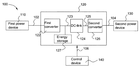
100361 FIG. 1 illustrates a block diagram of a system 100 in accordance
with an
exemplary embodiment of the present disclosure. The system 100 may be any
appropriate converter-based system that is capable of being configured to
implement the
new or improved nested NPP topology as disclosed herein. In some embodiments,
the
system 100 may be a multi-level converter-based system suitable for high power
and high
voltage applications. For example, the system 100 can be utilized in the
following areas,
including but not limited to, petro-chemistry, papermaking industry, mine,
power plant,
and water treatment plant, for driving one or more particular loads, such as
pump, fan,
and conveying device.
100371 As illustrated in FIG. 1, the system 100 generally includes a power
conversion device 120 and a control device 140 coupled in communication with
the
power conversion device 120. In one embodiment, the control device 140 is
arranged to
be in electrical communication with the power conversion device 120 and may
transmit
control signals 106 to the power conversion device 120 via one or more
electrical links or
wires for example. In another embodiment, the control device 140 may be in
optical
communication with the power conversion device 120 and can transmit the
control
signals 106 to the power conversion device 120 via an optical communication
link, such
as one or more optical fibers for example. The control device 140 may include
any
suitable programmable circuits or devices such as a digital signal processor
(DSP), a field
programmable gate array (FPGA), a programmable logic controller (PLC), and an
application specific integrated circuit (ASIC). The power conversion device
120 can be
operated to perform unidirectional or bidirectional power conversion between a
first
power device 110 and a second power device 130 in response to the control
signals 106
transmitted from the control device 140.
100381 In one embodiment, as shown in FIG. 1, the power conversion device
120
may include a first converter 122, a DC link 124, and a second converter 126.
In one
embodiment, the first converter 122 may be an AC-DC converter which is
configured to
convert first electric power 102 (e.g., first AC electric power) provided from
the first
9
CA 02840446 2014-01-23
267735
power device 110 (e.g., power grid) into DC electric power 123 (e.g., DC
voltage). In
some specific embodiments, the first converter 122 may employ the nested NPP
topology
which will be described in detail below with reference to FIG. 2. In one
embodiment, the
DC-link 124 may include multiple capacitors configured to filter first DC
voltage 123
provided from the first converter 122, and supply second DC voltage 125 to the
second
converter 126. In one embodiment, the second converter 126 may be a DC-AC
converter
which is configured to convert the second DC voltage 125 into a second AC
voltage 104,
and supply the second AC voltage 104 to the second power device 130 (e.g., AC
electric
motor). In one embodiment, the second converter 126 may be constructed with
controlled switch devices arranged to have the nested NPP topology which will
be
described in detail below with reference to FIG. 2. Although not illustrated
in FIG. 1, in
some embodiments, the system 100 may include one or more other devices and
components. For example, one or more filters and/or circuit breakers can be
placed
between the first power device 110 and the power conversion device 120. Also,
one or
more filters and/or circuit breakers can be placed between the power
conversion device
120 and the second power device 130.
[0039] In
other embodiments, the system 100 constructed with the new or improved
nested NPP topology disclosed herein can also be used in power generation
systems,
including but not limited to, wind power generation systems,
solar/photovoltaic power
generation systems, hydropower generation systems, and combinations thereof.
In one
embodiment, the first power device 110 may include one or more wind turbines
which
are configured to provide variable-frequency electric power. The first
converter 122 may
be an AC-DC converter and the second converter 126 may be a DC-AC converter,
such
that the variable-frequency electric power 102 can be converted into a fixed-
frequency
electrical power 104, for example, 50 Hertz or 60 Hertz AC power. The fixed-
frequency
electrical power 104 may be supplied to the second power device 130 such as a
power
grid for transmission and/or distribution. In some embodiments, the second
power device
130 may include a load such as an electric motor used in a vehicle, a fan, or
a pump,
which can be driven by the second electric power 104. In some embodiments,
when the
CA 02840446 2014-01-23
267735
system 100 is implemented as a solar power generation system, the first
converter 122
may be a DC-DC converter for performing DC electric power conversion. In some
occasions, the first converter 122 can be omitted, such that the second
converter or DC-
AC converter 126 is responsible for converting DC electric power provided from
the first
power device 110 (e.g., one or more solar panels) into AC electric power.
[0040] In some other embodiments, the system 100 may also be used in areas
that
are desirable to use uninterruptible/uninterrupted power system (UPS) for
maintaining
continuous power supply. In such applications, the power conversion device 120
of the
system 100 may also be configured to have the new or improved nested NPP
topology.
In one embodiment, the first converter 122 may be an AC-DC converter which is
configured to convert first AC electric power provided from the first power
device 110
(e.g., power grid) into DC electric power. The system 100 may also include an
energy
storage device 127 which is configured to receive and store the DC electric
power
provided from the first converter 122. In one embodiment, the second converter
126 may
be a DC-AC converter which is configured to convert the DC electric power
provided
from the first converter 122 or DC electric power obtained from the energy
storage
device 127 into second AC electric power, and supply the second electric power
to the
second power device 130 (e.g., a load).
[0041] Turning now to FIG. 2, which illustrates a detailed topology diagram
of a
converter 200 in accordance with an exemplary embodiment of the present
disclosure. In
one embodiment, the converter 200 can be used as the second converter 126, or
more
particularly, a DC-AC converter. In one embodiment, the converter 200 includes
a first
port 202 and a second port 204, both of which are configured to receive DC
voltage such
as the DC voltage 123 (see FIG. 1) provided from the first converter 122. The
first port
202 is electrically coupled a first DC line 206, and the second port 204 is
electrically
coupled to a second DC line 208. A DC-link 210 is also electrically coupled
between the
first port 202 and the second port 204 for performing filtering operations
with respect to
the received DC voltage and maintaining substantially constant voltage for
subsequent
11
CA 02840446 2014-01-23
267735
switch devices coupled thereto. In one embodiment, the DC-link 210 includes a
first
capacitor 212 and a second capacitor 214 coupled in series between the first
DC line 206
and the second DC line 208. A DC middle point 216 is defined between the first
capacitor 212 and the second capacitor 214. In other embodiments, the DC-link
210 may
include more than two capacitors, and at least part of the capacitors can be
coupled in
series or in parallel.
[0042] With continuing reference to FIG. 2, the converter 200 comprises a
first
phase leg 220, a second phase leg 250, and a third phase leg 280. Each of the
three phase
legs 220, 250, 280 is electrically coupled between the first DC line 206 and
the second
DC line 208 for receiving DC voltage provided from the DC link 210 and
providing
output voltage at its corresponding output port. More specifically, in one
embodiment,
the first phase leg 220 provides a first phase AC voltage through first output
port 235, the
second phase leg 250 provides a second phase AC voltage through second output
port
265, and the third phase leg 280 provides a third phase AC voltage through
third output
port 295. The first phase AC voltage, the second phase AC voltage, and the
third phase
AC voltage are offset from one another by 120 degrees. It should be understood
that,
when the converter 200 is implemented as an AC-DC converter, the three output
ports
235, 265, 295 can be configured to receive input AC voltages. Thus, the three
output
ports 235, 265, 295 can be generally referred to as AC ports. Similarly, the
first port 202
and the second port 204 can also be configured to output DC voltage, in which
case the
two ports 202, 204 can be generally referred to as DC ports.
[0043] Please referring to FIG. 2 and FIG. 3 together, in one embodiment,
the first
phase leg 220 includes at least two converter modules that are constructed to
have the
same structure. The two converter modules are coupled together in a nested
manner to
achieve a higher level phase leg. More specifically, the first phase leg 220
includes a first
converter module 222 and a second converter module 224 coupled together in a
nested
manner. In one embodiment, the first converter module 222 can be configured to
provide
an output voltage having 2n1+1 levels, and the second converter module 224 can
be
12
CA 02840446 2014-01-23
267735
configured to provide an output voltage having 2n2+1 levels, where n1 and n2
are both
equal to or larger than one, and ni is equal to n2. In another embodiment, ni
can be
arranged to be different than n2. In the illustrated embodiment, the first
converter module
222 and the second converter module 224 are arranged to provide five-level
output
voltages. In particular, each of the first and second converter modules 222,
224 is
configured to have six connecting terminals for the purpose of connecting with
corresponding connecting terminals of other converter modules.
[0044] More
specifically, in one embodiment, the first converter module 222
includes a first longitudinal arm 201, a second longitudinal arm 203, and a
transverse arm
205. It should be noted that "longitudinal" and "transverse" used herein are
used for
reference only, and not intended to limit the scope of the invention to
specific
orientations. The first longitudinal arm 201 includes a first switch unit 228
which has
one end formed as first-longitudinal-arm first connecting terminal 237 and
another end
formed as first-longitudinal-arm second connecting terminal 218. The
second
longitudinal arm 203 includes a second switch unit 232 arranged in the same
direction as
the first switch unit 228. The second switch unit 232 has one end formed as
second-
longitudinal-arm first connecting terminal 241 and another end formed as
second-
longitudinal-arm second connecting terminal 229. The transverse arm 205
includes a
third switch unit 234 and a fourth switch unit 236 that are reversely coupled
in series.
The third switch unit 234 has one end formed as transvers-arm first connecting
terminal
226, and the fourth switch unit 236 has one end formed as transverse-arm
second
connecting terminal 239. In one embodiment, the transverse-arm second
connecting
terminal 239 is electrically connected to a flying-capacitor middle point 223
defined
between a first flying capacitor 225 and a second flying capacitor 227. In
addition, two
ends of the first flying capacitor 225 are electrically connected to the two
connecting
terminals 237, 239 respectively, and two ends of the second flying capacitor
227 are
electrically connected to the two connecting terminals 241, 239 respectively.
13
CA 02840446 2014-01-23
267735
100451 Similarly, the second converter module 224 includes a first
longitudinal arm
207, a second longitudinal arm 209, and a transverse arm 271. The first
longitudinal arm
207 includes a fifth switch unit 238 which has one end formed as first-
longitudinal-arm
first connecting terminal 217 and another end formed as first-longitudinal-arm
second
connecting terminal 211. The second longitudinal arm 209 includes a sixth
switch unit
242 arranged in the same direction as the fifth switch unit 238. The sixth
switch unit 242
has one end formed as second-longitudinal-arm first connecting terminal 221
and another
end formed as second-longitudinal-arm second connecting terminal 215. The
transverse
arm 271 includes a seventh switch unit 244 and an eighth switch unit 246 that
are
reversely coupled in series. The seventh switch unit 244 has one end formed as
transvers-arm first connecting terminal 219, and the eighth switch unit 246
has one end
formed as transverse-arm second connecting terminal 213. In one embodiment,
the
transverse-arm second connecting terminal 216 is electrically connected to a
DC-link
middle point 236 defined between the first capacitor 212 and the second
capacitor 214 of
the DC-link 210. In addition, two ends of the first capacitor 212 are
electrically
connected to the two connecting terminals 211, 213 respectively, and two ends
of the
second capacitor 214 are electrically connected to the two connecting
terminals 213, 215
respectively.
[00461 In the illustrated embodiment, it can be seen that a nested NPP
structure is
formed by electrically connecting the two connecting terminals 217, 237,
electrically
connecting the two connecting terminals 219, 239, and electrically connecting
the two
connecting terminals 241, 221. It can be understood that, in other
embodiments, similar
connection can be made to form higher level converter by connecting three or
more than
three six-terminal converter modules. In the illustrated embodiment, since the
first
converter 222 is arranged as an inner-most block, the three connecting
terminals 218,
226, 229 of the first converter 222 are commonly connected with the AC port
235 for
receiving or providing AC voltage. In addition, since the second converter 224
is
arranged as an outer-most block, the first-longitudinal-arm second connecting
terminal
211 is electrically connected to the first DC port 202 through the first DC
line 206, and
14
CA 02840446 2014-01-23
267735
the second-longitudinal-arm second connecting terminal 215 is electrically
connected to
the second DC port 204 through the second DC line 208, so as to receive or
provide DC
voltage.
[0047] With continuing reference to FIG. 2, the second phase leg 250 is
configured
with similar structure as the first phase leg 220. For example, the second
phase leg 250
also includes a first converter module 252 and a second converter module 254
that are
coupled together in a nested marmer. Each of the first and second converter
modules 252,
254 has six connection terminals for connecting to corresponding terminals of
other
converter module. The first converter module 252 includes four switch units
258, 262,
264, 266, and the second converter module 254 includes four switch units 268,
272, 274,
276. The four switch units 258, 262, 264, 266 are connected in series to form
a
longitudinal arm, and another four switch units 268, 272, 274, 276 are
connected in series
to form a transverse arm. Two ends of the longitudinal arm are electrically
connected to
the first DC line 206 and the second DC line 208 respectively. One end of the
transverse
arm is electrically connected to the DC middle point 216, and the other end of
the
transverse arm is electrically connected to a joint connection 263 defined
between the two
switch units 258, 262. In addition, the second phase leg 250 includes two
flying
capacitors 255, 257 connected in series to form a flying capacitor arm. The
two flying
capacitors 255, 257 define a flying-capacitor middle point 253 which is
electrically
connected to a joint connection defined between the two switch units 266, 274.
Another
end of the first flying capacitor 255 is connected to a joint connection
defined between
the two switch units 268, 258, and another end of the second flying capacitor
257 is
electrically connected to a joint connection defined between the two switch
units 262,
272.
[0048] With continuing reference to FIG. 2, the third phase leg 280 is
configured
with similar structure as the first phase leg 220. For example, the third
phase leg 280 also
includes a first converter module 282 and a second converter module 284 that
are coupled
together in a nested manner. Each of the first and second converter modules
282, 284 has
CA 02840446 2014-01-23
267735
six connection terminals for connecting to corresponding terminals of other
converter
module. The first converter module 282 includes four switch units 288, 292,
294, 296,
and the second converter module 284 includes four switch units 298, 302, 304,
306. The
four switch units 288, 298, 292, 302 are connected in series to form a
longitudinal arm,
and another four switch units 294, 296, 304, 306 are connected in series to
form a
transverse arm. Two ends of the longitudinal arm are electrically connected to
the first
DC line 206 and the second DC line 208 respectively. One end of the transverse
arm is
electrically connected to the DC middle point 216, and the other end of the
transverse
arm is electrically connected to a joint connection 293 defined between the
two switch
units 288, 292. In addition, the third phase leg 280 includes two flying
capacitors 285,
287 connected in series to form a flying capacitor arm. The two flying
capacitors 285,
287 define a flying-capacitor middle point 283 which is electrically connected
to a joint
connection defined between the two switch units 296, 304. Another end of the
first flying
capacitor 285 is connected to a joint connection defined between the two
switch units
298, 288, and another end of the second flying capacitor 287 is electrically
connected to a
joint connection defined between the two switch units 292, 302.
100491 In one
embodiment, each of the first phase leg 220, the second phase leg
250, and the third phase leg 280 is configured to provide output voltage of
five levels. In
particular, the switching states of the switch units in the first leg 220 are
shown below in
table 1.
16
CA 02840446 2014-01-23
267735
Table-1 Switching states of the first phase leg
Switching states
Output
First Second Third Fourth Fifth Sixth Seventh Eighth
voltage
switch switch switch switch switch switch switch switch
level unit unit unit unit unit unit unit unit
228 232 234 236 238 242 244 246
2 1 0 0 1 1 0 0 1
1 0 0 1 0 0 1 1
1
0 0 1 1 1 0 0 1
0 0 1 1 0 0 1 1
0 1 0 0 1 0 1 1 0
0 1 1 0 1 0 0 1
0 0 1 1 0 1 1 0
-1
0 1 1 0 0 0 1 1
-2 0 1 1 0 0 1 1 0
100501 It can be seen from table-1, the first phase leg 220 can be
controlled to
provide output voltage having five different levels of "2," "1," "0," "4," "1"
by
selectively controlling the switching states of the eight switch units in the
first phase leg
220. It also can be seen when the output voltage level is "2" or "-2," there
exists a sole
combination switching states for the eight switch units. In contrast, when the
output
voltage level is "1" and "-I," there exist two combination switching states
for the eight
17
CA 02840446 2014-01-23
267735
switch units. When the output voltage level is "0," there exist three
combination
switching states for the eight switch units. In some embodiments, the voltage
of the first
and second flying capacitors 285, 287 can be balanced by selectively using the
switching
states of the switch units. Furthermore, as shown in table-1, the switch units
of the first
phase leg 220 are switched on and/or off in a complementary pattern. For
example, the
switching states of first switch unit 228 and the second switch unit 234 are
switched in
opposite states. Likewise, each of the switch unit pairs 232, 234; 238, 244;
and 242, 246
are switched in opposite states.
100511 FIG. 4 illustrates waveforms of switching signals supplied to the
eight
switch units in the first phase leg 220 and corresponding voltage and current
waveforms
in accordance with an exemplary embodiment of the present disclosure. As shown
in
FIG. 4, the switch units of the first phase leg 220 can be further configured
to be switched
on and/or off in a non-complementary pattern. For example, when the output
voltage
level is transitioning from "1" to "2," the switching signal for the seventh
switch unit 244
(T2) becomes logic "0," while the switching signal for the fifth switch unit
238 (Ti)
becomes logic "1" after a short time delay td (also known as dead-zone time).
It is known
that it usually takes longer time to turn off a switch device than turn on a
switch device.
Thus, the purpose of introducing such a short time delay is to avoid a short-
circuit
condition of the two flying capacitors when both switch units are in the ON
state. In other
words, during such a time delay td, both the seventh switch unit 244 (T2) and
the fifth
switch unit 238 (Ti) are turned off, that is, the two switch units 244, 238
are controlled to
operate in a non-complementary pattern. After the time delay td, the seventh
switch unit
244 (T2) remains off and the fifth switch unit 238 (Ti) is turned on, in this
case, the two
switch units 244, 238 are controlled to operate in a complementary pattern.
[0052] With continuing reference to FIG. 4, in case the output voltage 563
has a
level of "1," the switching signal supplied to the fifth switch unit 238 (Ti)
is low level
signal. Conventionally, to ensure complementary switching, the switching
signal
supplied to the seventh switch unit 244 (T2) should be a high level signal. In
the
18
CA 02840446 2014-01-23
267735
illustrated embodiment, because electrical current can be flowing through the
anti-parallel
diode in association with the seventh switch unit 244 (T2), thus, the
switching signal
supplied to the seventh switch unit 244 (T2) can be temporarily blocked or
masked to
reduce switching numbers as well as reduce power loss due to the unnecessary
switching
actions. In this case, the fifth switch unit 238 and the seventh switch unit
244 are also
operated in a non-complementary pattern. Similarly, as shown in FIG. 4, the
fourth
switch unit 234 (S3) and the second switch unit 232 (S4) can also be operated
in
complementary pattern and non-complementary pattern due to the introduction of
delay
time td. Furthermore, as shown in FIG. 4, in one embodiment, during the single
switching control cycle starting from to to t8, the switching signals supplied
to the switch
units T2, T3, S2, S3 in the transverse arm are blocked in predetermined time
period, so as
to reduce switching numbers as well as power loss. In other embodiment,
switching
signals supplied to switch units Ti, T4, Si, S4 in the longitudinal arm can be
blocked to
reduce switching numbers as well as power loss.
[0053] FIG. 5 illustrates an output voltage waveform 560 of the converter
shown in
FIG. 2 in accordance with an exemplary embodiment of the present disclosure.
As
shown in FIG. 5, with the use of converter having a nested NPP topology, one
phase leg
of the converter can provide output voltage having five levels with good
waveforms.
[0054] FIG. 6 illustrates a schematic diagram of a first type switch unit
310
contained in the converter as shown in FIG. 2 in accordance with an exemplary
embodiment of the present disclosure. In one embodiment, the first type switch
unit 310
can be any one of the switch units in the longitudinal arm of the three phase
legs. In a
particular embodiment, the first four switch units 238, 228, 232, 242 in the
longitudinal
arm of the first phase leg 220 can be configured to be exactly the same as the
switch unit
310. More specifically, in one embodiment, the switch unit 310 may include a
single
switch device or include multiple series-connected switch devices. For
example, in one
embodiment, the switch unit 310 includes a first switch device 316, a second
switch
device 318, and a pth switch device 322, where p is equal to or larger than
two. In
19
CA 02840446 2014-01-23
267735
addition, in one embodiment, the first switch device 316 is connected in
parallel with a
first anti-parallel diode 324, the second switch device 318 is connected in
parallel with a
second anti-parallel diode 326, and the IP switch device 322 is connected in
parallel with
h
t
a p anti-parallel diode 328. In some conditions, each switch device can be
integrated
with the anti-parallel diode to form a single device. Because the first switch
device 316,
the second switch device 318, and the pth switch device 322 are connected in
series
between the DC lines 206, 208, each of the switch devices is applied with a
portion of the
DC voltage. Thus, low nominal voltage switch device can be used to replace a
single
switch device 312 (as shown in FIG. 6, the single switch device 312 is also
integrated
with an anti-parallel diode 314) which has a high nominal voltage. Non-
limiting
examples of the switch device that may be used in the converter may include
metal oxide
semiconductor field effect transistor (MOSFET), insulated gate bipolar
transistor (IGBT),
and integrated gate commutated thyristor (IGCT).
100551 FIG. 7
illustrates a schematic diagram of a first type switch unit 320 in
accordance with another exemplary embodiment of the present disclosure. The
first type
switch unit 320 shown in FIG. 7 is substantially similar to the first type
switch unit 310
shown in FIG. 6. For example, the first type switch unit 320 also includes a
first switch
device 316, a second switch device 318, and a pth switch device 322, where p
is equal to
or larger than two. The first type switch unit 320 also includes a first anti-
parallel diode
324, a second anti-parallel diode 326, and a pth anti-parallel diode 328, each
of which is
coupled in parallel with a corresponding switch device. In addition, the first
type switch
unit 320 further includes a first snubber circuit 323 arranged in association
with the first
switch device 316, a second snubber circuit 325 arranged in association with
the second
switch device 318, and a third snubber circuit 327 arranged in association
with the third
switch device 322. In a particular embodiment, the first, second, and third
snubber
circuits 323, 325, 327 can be formed by one or more passive electronic devices
such as
capacitors, resistors, and so on. The purpose of providing these snubber
circuits 323,
325, 327 is to ensure voltage to be shared equally among the switch devices
316, 318,
322 during the dynamic switching processes.
CA 02840446 2014-01-23
267735
[0056] FIG. 8 illustrates a schematic diagram of a second type switch unit
330 used
in the converter shown in FIG. 2 in accordance with an exemplary embodiment of
the
present disclosure. In one embodiment, the second type switch unit 330 can be
any one
of the switch unit in the transverse arm of the three phase legs. In a
particular
embodiment, the first four switch units 234, 236, 244, 246 in the transverse
arm of the
first phase leg 220 can be configured to be exactly the same as the switch
unit 320. More
specifically, in one embodiment, the switch unit 320 includes a first switch
device 336, a
second switch device 338, and an mth switch device 342, where m is equal to or
larger
than two. In addition, in one embodiment, the first switch device 336 is
connected in
parallel with a first anti-parallel diode 344, the second switch device 338 is
connected in
parallel with a second anti-parallel diode 346, and the mth switch device 342
is connected
in parallel with an mth anti-parallel diode 348. In some conditions, each
switch device
can be integrated with the anti-parallel diode to form a single device.
Because the first
switch device 316, the second switch device 318, and the mth switch device 342
are
connected in series between the DC lines 206, 208, each of the switch devices
is applied
with a portion of the DC voltage. Thus, low nominal voltage switch device can
be used
to replace a single switch device 332 (as shown in FIG. 8, the single switch
device 332 is
also integrated with an anti-parallel diode 334) which has a high nominal
voltage. Non-
limiting examples of the switch device that may be used in the converter may
include
metal oxide semiconductor field effect transistor (MOSFET), insulated gate
bipolar
transistor (IGBT), and integrated gate commutated thyristor (IGCT).
[0057] In some embodiments, the switch devices 336, 338, 342 in the second
type
switch unit 330 can be arranged to be the same as the switch devices 316, 318,
322. In
other embodiments, different switch devices having different voltage ratings
can be used.
In addition, in some embodiments, the number of the switch devices arranged in
the first
type switch unit 310 can be the same as or different from the number of switch
devices
arranged in the second type switch unit 330. In some embodiments, the exact
number of
the switch devices used in the first or second switch units 310, 330 can be
determined
21
CA 02840446 2014-01-23
267735
based on associated operating parameters of the converter, such as DC-link
voltages and
nominal voltages of the switch devices.
[00581 FIG. 9 illustrates a schematic diagram of a second type switch unit
340 in
accordance with another exemplary embodiment of the present disclosure. The
second
type switch unit 340 shown in FIG. 9 is substantially similar to the second
type switch
unit 330 shown in FIG. 8. More specifically, in one embodiment, the switch
unit 340
may include a single switch device or include multiple series-connected switch
devices.
For example, in one embodiment, the second type switch unit 340 also includes
a first
switch device 336, a second switch device 338, and an Mth switch device 342,
where m is
equal to or larger than two. The second type switch unit 340 also includes a
first anti-
parallel diode 344, a second anti-parallel diode 346, and an mth anti-parallel
diode 348,
each of which is coupled in parallel with a corresponding switch device. In
addition, the
second type switch unit 340 further includes a first snubber circuit 343
arranged in
association with the first switch device 336, a second snubber circuit 345
arranged in
association with the second switch device 338, and a third snubber circuit 347
arranged in
association with the third switch device 342. In a particular embodiment, the
first,
second, and third snubber circuits 343, 345, 347 can be formed by one or more
passive
electronic devices such as capacitors, resistors, and so on. The purpose of
providing
these snubber circuits 343, 345, 347 is to ensure voltage to be shared equally
among the
switch devices 336, 338, 342 during the dynamic switching process.
[0059] FIG. 10 illustrates a schematic diagram of one phase leg of a
converter in
accordance with another exemplary embodiment of the present disclosure. In
particular,
the single phase leg 400 shown in FIG. 10 can be used to replace one or more
of the three
phase legs 220, 250, 280 shown in FIG. 2. In the illustrated embodiment, the
single
phase leg 400 is configured to provide an output voltage having seven levels.
As shown
in FIG. 10, the single phase leg 400 includes a first port 402 and a second
port 404 for
receiving or providing DC voltages. The single phase leg 400 also includes a
DC-link
460 for filtering the DC voltages and providing substantially constant voltage
to the
22
CA 02840446 2014-01-23
267735
switch unit or switch devices connected to the DC-link 460. The single phase
leg 400
also includes a third port 405 for providing or receiving AC voltages. In one
embodiment, the DC-link 460 is electrically coupled between a first DC line
406 and a
second DC line 408, and the first DC-link 406 includes a first capacitor 462
and a second
capacitor 464 connected in series.
100601
Referring to FIG. 10, the single phase leg 400 also includes a first converter
module 410, a second converter module 420, and a third converter module 430
connected
in a nested manner substantially similar to the single phase leg 220 shown in
FIG. 3. In
the illustrated embodiment, each of the three converter modules 410, 420, 430
is
configured to provide three-level output voltage, such that the single phase
leg 400 can
provide seven-level output voltage. In other embodiments, the single phase leg
can also
be constructed by nesting a five-level converter module with a three-level
converter
module. Similar to the single phase leg 220 shown in FIG. 3, each of the three
converter
modules 410, 420, 430 is arranged to have six connecting terminals for
connecting to
corresponding connecting terminals of other converter modules. As shown in
FIG. 10,
the first converter module 410 includes four switch units 412, 414, 416, 418,
the second
converter module 420 includes four switch units 422, 424, 426, 428, and the
third
converter module 430 includes four switch units 432, 434, 436, 438. Of these
switch
units, six switch units 432, 422, 412, 414, 424, 434 are connected in series
to form a
longitudinal arm, another six switch units 438, 436, 428, 426, 418, 416 are
connected in
series to form a transverse arm. One end of the transverse arm is electrically
connected to
DC middle point 412 of the DC link 460, and the other end of the transverse
arm is
electrically connected to a joint connection defined between the two switch
units 412,
414. The single phase leg 400 also includes a first flying capacitor 442 and a
second
flying capacitor 444 connected in series to form a first flying capacitor arm
440. The
single phase leg 400 also includes a third flying capacitor 452 and a fourth
flying
capacitor 454 connected in series to form a second flying capacitor arm 450.
One end of
the first flying capacitor 442 and one end of the second flying capacitor 444
are
commonly connected to joint connection 443 defined between the two switch
units 418,
23
CA 02840446 2014-01-23
267735
426. The other end of the first flying capacitor 442 is connected to joint
connection
defined between the two switch units 422, 412, and the other end of the second
flying
capacitor 444 is connected to a joint connection defined between the two
switch units
414, 424. One end of the third flying capacitor 452 and one end of the fourth
flying
capacitor 454 are commonly connected to joint connection 453 defined between
the two
switch units 436, 428. The other end of the third flying capacitor 452 is
connected to
joint connection defined between the two switch units 432, 422, and the other
end of the
fourth flying capacitor 454 is connected to a joint connection defined between
the two
switch units 424, 434.
[0061] FIG.
11 illustrates a schematic diagram of at least a part of a grid side or
rectifier side (generally designated as 620) of the power conversion system
shown in FIG.
1 in accordance with an exemplary embodiment of the present disclosure. As
illustrated
in FIG. 11, the grid side or rectifier side 620 includes a first converter or
more
specifically an AC-DC converter 624, which is configured to have a nested
neutral point
piloted topology as shown in FIG. 2 and FIG. 3. The first converter or the AC-
DC
converter 624 can be configured to operate on four quadrants, that is, bi-
directional power
conversion can be achieved. In one embodiment, the AC-DC converter 624 is
configured
to convert electrical power (e.g., single-phase, three-phase, and/or multi-
phase electrical
power) provided from an input energy device 622 such as a power grid to DC
electrical
power, and supply the DC electrical power to a DC-link 626. In one embodiment,
the
DC-link 626 includes a first capacitor 623 and a second capacitor 625 coupled
in series.
In other embodiments, the AC-DC converter 624 can also be configured to
convert DC
electrical power provided from the DC-link 626 into AC electrical power, and
feed the
AC electrical power to the input energy device 622. In a particular
embodiment, the
input energy device 622 can be a power grid which is configured to provide
three-phase
AC voltages of 6KV, 6.6KV, 10KV for example. The input energy device or the
power
grid 622 is electrically coupled to the first converter or the AC-DC converter
624 via a
first-phase line 638, a second-phase line 642, and a third-phase line 644. The
first-phase
line 638 is configured to deliver first-phase AC voltage between the power
gird 622 and
24
CA 02840446 2014-01-23
267735
the first converter 624, the second-phase line 642 is configured to deliver
second-phase
AC voltage between the power grid 622 and the first converter 624, and the
third-phase
line 644 is configured to deliver third-phase AC voltage between the power
grid 622 and
the first converter 624. In one embodiment, the three-phase AC voltages being
delivered
through the three-phase lines 638, 642, 644 are offset from one another by 120
degrees.
100621 With continuing reference to FIG. 11, in one embodiment, the grid
side or
rectifier side 620 further includes a first filter 630 (also can be referred
to as input filter)
which is electrically coupled between the power grid 622 and the first
converter 624. As
can be understood, in one embodiment, coupling the first converter 624 to the
power grid
622 through the first filter 630 can help avoid a conventionally used
transformer, thereby
the cost and volume of the system can be substantially reduced. In one
embodiment, the
first filter 630 includes a differential-mode (DM) filter, which, in one
aspect, can be
configured to remove harmonic signals contained in the three-phase AC voltages
provided from the power grid 622. Therefore, negative impact caused from the
harmonic
signals on the first converter 624 can be mitigated. In another aspect, the
first filter 630
can also be configured to remove harmonic signals generated by the first
converter 624 so
as to meet relevant grid standards.
[0063] In the illustrated embodiment of FIG. 11, the first filter or the DM
filter 630
includes a first-phase first inductor 632, a second-phase first inductor 634,
and a third-
phase first inductor 636. The first-phase first inductor 632 is attached to or
electrically
coupled to the first-phase line 638 arranged between the power grid 622 and
the first
converter 624. The second-phase first inductor 634 is attached to or
electrically coupled
to the second-phase line 642 arranged between the power grid 622 and the first
converter
624. The third-phase first inductor 636 is attached or electrically coupled to
the third-
phase line 644 arranged between the power grid 622 and the first converter
624. In one
embodiment, the first filter or the DM filter 630 further includes a first
branch line 650, a
second branch line 660, and a third branch line 670. The first branch line 650
has one
terminal connected to the first-phase line 638, the second branch line 660 has
one
CA 02840446 2014-01-23
267735
terminal connected to the second-phase line 642, and the third branch line 670
has one
terminal connected to the third-phase line 644. The other ends of the first,
second, and
third branch lines 650, 660, 670 are commonly connected to form a joint
connection point
676.
100641 In one embodiment, the first branch line 650 includes a first
resistor (also
known as damping resistor) 652 and a first capacitor 654 coupled in series,
the second
branch line 660 includes a second resistor 662 and a second capacitor 664
coupled in
series, and the third branch line 670 includes a third resistor 672 and a
third capacitor 674
coupled in series. In other embodiments, the first resistor 652 used in first
branch line
650, the second resistor 662 used in the second branch line 660, and the third
resistor 672
used in the third branch line 670 can be removed. In practical implementation,
the
inductors can be selected to have appropriate inductance, the capacitors can
be selected to
have appropriate capacitance, and the resistors can be selected to have
appropriate
resistance for effective filtering of harmonic signals. In some embodiments,
the first
filter 630 can be arranged to have its joint connection point 676 being
commonly
grounded with respect to one or more load-side or machine-side filters. For
example, the
DM filter 630 can be grounded when the electric motor can withstand common
mode
stress. In such a case, the common mode voltage is transferred to the machine
side, and
the machine-side filter can also be grounded to reduce the common-mode stress,
thereby
one or more common-mode filter can be eliminated. Consequently, in some cases,
common mode voltage standard of the grid still can be met without using the
common-
mode filter, thereby the system efficiency and power density can be improved,
and the
cost can be reduced.
[0065] FIG. 12 illustrates a schematic diagram of at least a part of a grid
side or
rectifier side of the power conversion system shown in FIG. 1 in accordance
with another
exemplary embodiment of the present disclosure. The arrangements of the grid
side 620
shown in FIG. 12 are substantially similar to what has been shown and
described with
reference to FIG. 11. Thus, elements in FIG. 12 designated with the same
reference
26
CA 02840446 2014-01-23
267735
numerals as that shown in FIG. 11 will not be described in detail. In
particular, in the
embodiment shown in FIG. 12, the first filter 630 of the grid side or
rectifier side 620
may further include a first-phase second inductor 682, a second-phase second
inductor
684, and a third-phase second inductor 686. The first-phase second inductor
682 is
electrically connected in series with the first-phase first inductor 632, and
is attached to or
electrically connected to the first-phase line 638. The second-phase second
inductor 684
is electrically connected in series with the second-phase first inductor 634,
and is attached
to or electrically connected to the second-phase line 642. The third-phase
second
inductor 686 is electrically connected in series with the third-phase first
inductor 636, and
is attached to or electrically connected to the third-phase line 644. In some
specific
embodiments, each of the three-phase second inductors 682, 684, 686 is
arranged to have
a smaller inductance than each of the three-phase first inductors 632, 634,
636, to make
sure the capacity or power of the power gird 622 can match that of the first
converter 624.
In other words, when the capacity or power of the power grid 622 and the first
converter
624 are matched, the three-phase second inductors 682, 684, 686 can be
omitted.
100661 FIG.
13 illustrates a schematic diagram of at least a part of a grid side or
rectifier side of the power conversion system shown in FIG. 1 in accordance
with another
exemplary embodiment of the present disclosure. The arrangements of the grid
side 620
shown in FIG. 13 are substantially similar to what has been shown and
described with
reference to FIG. 11. Thus, elements in FIG. 13 designated with the same
reference
numerals as that shown in FIG. 11 will not be described in detail. In
particular, in the
embodiment shown in FIG. 13, the grid side 620 further includes a second
filter 690
which is coupled in series with the first filter 630, and is electrically
coupled between the
power grid 622 and the first converter 624. In one embodiment, the second
filter 690
includes a common-mode (CM) filter which includes a first CM inductor 692, a
second
CM inductor 694, and a third CM inductor 696. The first, second, and third CM
inductors 692, 694, 696 are magnetically coupled together with dots shown on
the same
side. In the illustrated embodiments, the three dots are arranged at a side
adjacent to the
first converter 624. In other embodiments, the three dots can also be arranged
at another
27
CA 02840446 2014-01-23
267735
side adjacent to the power grid 622. The second filter or the CM filter 690 is
configure to
remove common-mode signals transmitting along the three-phase lines 638, 642,
644
arranged between the power grid 622 and the first converter 624. As a result,
common-
mode voltage standards of the power grid can be met, and the conventionally
used
transformer can be totally removed or eliminated.
100671 FIG. 14 illustrates a schematic diagram of at least a part of a grid
side or
rectifier side of the power conversion system shown in FIG. 1 in accordance
with another
exemplary embodiment of the present disclosure. The arrangements of the grid
side 620
shown in FIG. 14 are substantially similar to what has been shown and
described with
reference to FIG. 11. Thus, elements in FIG. 14 designated with the same
reference
numerals as FIG. 11 will not be described in detail. In particular, in the
embodiment
shown in FIG. 14, the grid side 620 further includes three-phase second
inductors 682,
684, 686 for matching power or capacity between the power grid 622 and the
first
converter 624. In addition, in the embodiment shown in FIG. 19, the grid side
620
further includes a second filter 690. In one embodiment, the second filter 690
includes a
CM filter which includes three CM inductors 692, 694, 696 for removing common
mode
signals.
[00681 FIG. 15 illustrates a schematic diagram of at least a part of a grid
side or
rectifier side of the power conversion system shown in FIG. 1 in accordance
with another
exemplary embodiment of the present disclosure. The arrangements of the grid
side 620
shown in FIG. 15 are substantially similar to what has been shown and
described with
reference to FIG. 11. Thus, elements in FIG. 15 designated with the same
reference
numerals as FIG. 11 will not be described in detail. In particular, in the
embodiment
shown in FIG. 16, the first filter or the DM filter 630 at the grid side 620
may be shunt
filter used for filtering one or more harmonic signals at the grid side 630.
In one
embodiment, the shunt filter 630 includes a first phase branch line 651, a
second phase
branch line 653, and a third phase branch line 655. The first phase branch
line 651 is
electrically coupled to the first phase line 638, the second phase branch line
653 is
28
CA 02840446 2014-01-23
267735
electrically coupled to the second phase line 642, and the third phase branch
line 655 is
electrically coupled to the third phase line 644. In one embodiment, the first
phase
branch line 651 includes a first shunt inductor 663 and a first shunt
capacitor 667 coupled
in series, the second phase branch line 653 includes a second shunt inductor
665 and a
second shunt capacitor 659 coupled in series, and the third phase branch line
655 includes
a third shunt inductor 667 and a third capacitor 661. In the illustrated
embodiment, the
three phase branch lines 651, 653, 655 are commonly connected to a joint
connection 669
which may be selectively grounded. In particular, in some embodiments, it may
be
desirable to filter multiple harmonic signals, for example, 5th order harmonic
signal, 7th
order harmonic signal, 11th order harmonic signal, and 13th harmonic signal.
In this
situation, each of the three phase branch lines 651, 653, 655 may include four
sub-branch
lines, and the shunt inductor and shunt capacitor in each sub-branch line can
be
configured to have appropriate inductance and capacitance for effectively
removing the
corresponding 5th order harmonic signal, 7th order harmonic signal, 11th order
harmonic
signal, and 13th harmonic signal. In addition, in some embodiments, the shunt
filter 630
as described herein may be used in combination with the main-branch inductors
632, 634,
636 for more effectively removing the harmonic signals.
[0069] FIG.
16 illustrates a schematic diagram of at least a part of a grid side or
rectifier side of the power conversion system shown in FIG. 1 in accordance
with another
exemplary embodiment of the present disclosure. The arrangements of the grid
side 620
shown in FIG. 16 are substantially similar to what has been shown and
described with
reference to FIG. 11. Thus, elements in FIG. 16 designated with the same
reference
numerals as FIG. 11 will not be described in detail. In particular, in the
embodiment
shown in FIG. 16, the grid side 620 further includes three-phase second
inductors 682,
684, 684 for matching power or capacity between the power grid 622 and the
first
converter 624. Moreover, the grid side 620 further includes a second filter
691. In one
embodiment, the second filter 690 includes a common-mode (CM) filter which
includes a
first CM inductor 693 and a second CM inductor 695. The first and second CM
inductors
693 and 695 are magnetically coupled together with two dots arranged on the
same side.
29
CA 02840446 2014-01-23
267735
In the illustrated embodiment, the two dots are arranged at a side adjacent to
the DC-link
626. In other embodiments, the two dots may be arranged at another side
adjacent to the
first converter 624.
100701 FIG. 17 illustrates a schematic diagram of at least a part of a load
side or
machine side of the power conversion system shown in FIG. 1 in accordance with
an
exemplary embodiment of the present disclosure. In the illustrated embodiment,
the load
side or machine side 710 includes a second converter or more particularly an
inverter 712
which is electrically coupled between the DC-link 626 and a load 714. In one
embodiment, the DC-link 626 includes a first capacitor 623 and a second
capacitor 625
coupled in series. In one embodiment, the load 714 may include an AC electric
motor,
for example, a three-phase AC electric motor. In one embodiment, the second
converter
or inverter 712 is arranged to have a nested neutral point piloted topology as
shown in
FIG. 2. The second converter or inverter 712 is configured to convert DC
voltage
provided from the DC-link 626 to AC voltage (e.g., three-phase AC voltage). In
one
embodiment, the second converter 712 is electrically connected to the three-
phase AC
electric motor 714 through a first-phase line 716, a second-phase line 718,
and a third-
phase line 722 to supply three-phase AC voltages for driving the three-phase
AC electric
motor 714.
[0071] With continuing reference to FIG. 17, in one embodiment, the load
side or
machine side 710 further includes a load-side filter 720 which is electrically
coupled
between the second converter 712 and the three-phase AC electric motor 714.
The load-
side filter 720 is configured to remove harmonic signals contained in the
three-phase AC
voltages generated from the second converter 712 to reduce negative impact on
the three-
phase AC electric motor 714. In one embodiment, the load-side filter 720
includes a
first-phase inductor 724, a second-phase inductor 726, and a third-phase
inductor 728.
The first-phase inductor 724 is attached to or electrically coupled to the
first-phase line
716 arranged between the second converter 712 and the three-phase AC electric
motor
714. The second-phase inductor 726 is attached to or electrically coupled to
the second-
CA 02840446 2014-01-23
267735
phase line 718 arranged between the second converter 712 and the three-phase
AC
electric motor 714. The third-phase inductor 728 is attached to or
electrically coupled to
the third-phase line 722 arranged between the second converter 712 and the
three-phase
AC electric motor 714.
(0072] In one
embodiment, the load-side filter 720 further includes a first branch
line 730, a second branch line 740, and a third branch line 750. The first
branch line 730
has one terminal connected to the first-phase line 716, the second branch line
740 has one
terminal connected to the second-phase line 718, and the third branch line 750
has one
terminal connected to the third-phase line 722. In addition, the other
terminals of the
three branch lines 730, 740, 750 are commonly connected to form a joint
connection
point 733. In one embodiment, the first branch line 730 includes a first
resistor 732 and a
first capacitor 734 coupled in series, the second branch line 740 includes a
second resistor
742 and a second capacitor 744 coupled in series, and the third branch line
750 includes a
third resistor 752 and a third capacitor 754 coupled in series. In
practical
implementations, the three inductors 724, 726, 728 can be arranged to have
appropriate
inductance, the three resistors 732, 742, 752 can be arranged to have
appropriate
resistance, and the three capacitors 734, 744, 754 can be arranged to have
appropriate
capacitance, such that the harmonic signals can be effectively removed. As
noted above,
when the three-phase AC electric motor 714 can withstand the common-mode
stress, the
load-side filter 720 can be commonly grounded with respect to the grid-side
filter 690 or
691. In such as case, the common-mode filter 690 or 691 (shown in FIGS. 13-16)
can be
eliminated. Therefore, common-mode voltage standards of the grid can be met,
efficiency and power density of the system can be improved, and cost can be
reduced.
[0073] With
continuing reference to FIG. 17, in the illustrated embodiment, the
load-side 710 further includes an equivalent impedance circuit 760 which
represents the
impedance of the three-phase lines arranged between the second converter 624
and the
three-phase AC electric motor 714. In one embodiment, the equivalent impedance
circuit
760 takes a form of first-order circuit. In other embodiments, the equivalent
impedance
31
CA 02840446 2014-01-23
267735
circuit 760 can be multi-order circuit. In the illustrated embodiment, the
equivalent
impedance circuit 760 includes a first-phase inductor 762, a second-phase
inductor 764,
and a third-phase inductor 766, a first capacitor 768, a second capacitor 772,
and a third
capacitor 774.
100741 FIG. 18 illustrates a flowchart of a power conversion method 800 in
accordance with an exemplary embodiment of the present disclosure. In some
embodiments, a power conversion system configured to have a transformerless
structure
is used for perform power conversion operations. More specifically, in such as
a
transformerless power conversion system, a first converter or a grid-side
converter
arranged to have a nested neutral point piloted topology is coupled to a power
gird
through one or more grid-side filters, thereby conventionally used transformer
can be
eliminated.
100751 In one embodiment, the method 800 may start to implement from block
802.
At block 802, first AC voltage provided from the power grid and filtered
through a grid-
side filter is received, and the first AC voltage is not processed by a
transformer. In one
embodiment, the first AC voltage is a three-phase AC voltage. The grid-side
filter may
include a differential-mode filter or further include a common-mode filter.
100761 The method 800 may further include a block 804. At block 804, a
first
converter or an AC-DC converter having the nested neutral point piloted
topology is used
to convert the first AC voltage into DC voltage. In one embodiment, the five-
level
converter 200 shown in FIG. 2 and FIG. 3 can be used to perform such an AC-DC
power
conversion. In some embodiments, the DC voltage provided from the AC-DC
converter
may be supplied to a DC-link to perform filtering operations. In some other
embodiments, a common-mode filter may be used to filter common mode signals
from
the DC voltage.
[0077] The method 800 may further include a block 806. At block 806, a
second
converter or a DC-AC converter is used to convert the DC voltage into second
AC
32
CA 02840446 2014-01-23
267735
voltage. In one embodiment, the five-level converter 200 shown in FIG. 2 and
FIG. 3 can
be used to perform such DC-AC power conversion.
[0078] The method 800 may further include a block 808. At block 808, the
second
AC voltage is supplied to a load, for example, an AC electric machine. When
the AC
electric machine is a three-phase AC electric machine, the second AC voltage
can be a
three-phase AC voltage.
[0079] While the invention has been described with reference to exemplary
embodiments, it will be understood by those skilled in the art that various
changes may
be made and equivalents may be substituted for elements thereof without
departing from
the scope of the invention. Furthermore, the skilled artisan will recognize
the
interchangeability of various features from different embodiments. Similarly,
the various
method steps and features described, as well as other known equivalents for
each such
methods and feature, can be mixed and matched by one of ordinary skill in this
art to
construct additional assemblies and techniques in accordance with principles
of this
disclosure. In addition, many modifications may be made to adapt a particular
situation
or material to the teachings of the invention without departing from the
essential scope
thereof Therefore, it is intended that the invention not be limited to the
particular
embodiment disclosed as the best mode contemplated for carrying out this
invention, but
that the invention will include all embodiments falling within the scope of
the appended
claims.
33