Note: Descriptions are shown in the official language in which they were submitted.
CA 02840498 2013-12-24
WO 2013/003850
PCT/US2012/045272
1
DESCRIPTION
A METHOD AND APPARATUS FOR DETECTING INFRARED RADIATION WITH
GAIN
CROSS-REFERENCE TO RELATED APPLICATION
The present application claims the benefit of U.S. Provisional Patent
Application
Serial No. 61/503,317, filed June 30, 2011, the disclosure of which is hereby
incorporated by
reference in its entirety, including any figures, tables, or drawings.
BACKGROUND OF INVENTION
Infrared (IR) light is not visible to the human eye, but an IR photodetector
can detect
IR light. IR photodetectors have a wide range of potential applications,
including night
vision, range finding, security, and semiconductor wafer inspections. IR can
refer to
radiation having wavelengths longer than visible light (>0.7 [tm) up to about
14 um.
BRIEF SUMMARY
Embodiments of the subject invention relate to a photodetector capable of
producing
gain (i.e., a photodetector with gain). The photodetector can be, for example,
an infrared (IR)
photodetector. That is, the photodetector can be sensitive to at least a
portion of light in the
IR region. Embodiments of the subject invention also pertain to an IR-to-
visible
upconversion device. The IR-to-visible upconversion device can include a
photodetector and
an organic light-emitting device (OLED).
In an embodiment, a photodetector with gain can include a first electrode, a
light
sensitizing layer on the first electrode, an electron blocking/tunneling layer
on the light
sensitizing layer, and a second electrode on the electron blocking/tunneling
layer.
In another embodiment, a method of fabricating a photodetector with gain can
include: forming a first electrode; forming a light sensitizing layer on the
first electrode;
forming an electron blocking/tunneling layer on the light sensitizing layer;
and forming a
second electrode on the electron blocking/tunneling layer.
In another embodiment, an IR-to-visible upconversion device can include a
photodetector with gain and an OLED coupled to the photodetector with gain.
The
photodetector with gain can include a first electrode, a light sensitizing
layer on the first
SUBSTITUTE SHEET (RULE 26)
CA 02840498 2013-12-24
WO 2013/003850
PCT/US2012/045272
2
electrode, an electron blocking/tunneling layer on the light sensitizing
layer, and a second
electrode on the electron blocking/tunneling layer.
In another embodiment, a method of forming an IR-to-visible upconversion
device
can include: forming a photodetector with gain; forming an OLED; and coupling
the OLED
to the photodetector with gain. Forming the photodetector with gain can
include: forming a
first electrode; forming a light sensitizing layer on the first electrode;
forming an electron
blocking/tunneling layer on the light sensitizing layer; and forming a second
electrode on the
electron blocking/tunneling layer.
BRIEF DESCRIPTION OF DRAWINGS
Figure lA shows an absorption spectrum of PbS nanocrystals which can be used
as
an IR sensitizing layer according to an embodiment of the subject invention.
Figure 1B shows a schematic perspective view of a photodetector according to
an
embodiment of the subject invention.
Figure 2A shows a schematic energy band diagram of a photodetector, according
to
an embodiment of the subject invention, under applied voltage in the dark.
Figure 2B shows a schematic energy band diagram of a photodetector, according
to
an embodiment of the subject invention, under applied voltage and IR
irradiation.
Figure 3A shows a schematic energy band diagram of a photodetector according
to
an embodiment of the subject invention.
Figure 3B shows current vs. voltage characteristics for a photodetector
according to
an embodiment of the subject invention under dark and photo (1240 nm infrared
illumination) conditions.
Figure 4A shows a plot of gain as a function of applied voltage for a
photodetector
according to an embodiment of the subject invention.
Figure 4B shows a plot of detectivity as a function of applied voltage on a
photodetector according to an embodiment of the subject invention.
Figure 5A shows a schematic energy band diagram of an infrared-to-visible
upconversion device according to an embodiment of the subject invention.
Figure 5B shows a schematic energy band diagram of an infrared-to-visible
upconversion device according to an embodiment of the subject invention.
Figure 5C shows a schematic energy band diagram of an infrared-to-visible
upconversion device according to an embodiment of the subject invention.
SUBSTITUTE SHEET (RULE 26)
CA 02840498 2013-12-24
WO 2013/003850
PCT/US2012/045272
3
DETAILED DISCLOSURE
When the terms "on" or "over" are used herein, when referring to layers,
regions,
patterns, or structures, it is understood that the layer, region, pattern or
structure can be
directly on another layer or structure, or intervening layers, regions,
patterns, or structures
may also be present. When the terms "under" or "below" are used herein, when
referring to
layers, regions, patterns, or structures, it is understood that the layer,
region, pattern or
structure can be directly under the other layer or structure, or intervening
layers, regions,
patterns, or structures may also be present. When the term "directly on" is
used herein, when
referring to layers, regions, patterns, or structures, it is understood that
the layer, region,
pattern or structure is directly on another layer or structure, such that no
intervening layers,
regions, patterns, or structures are present.
When the term "about" is used herein, in conjunction with a numerical value,
it is
understood that the value can be in a range of 95% of the value to 105% of the
value, i.e. the
value can be +/- 5% of the stated value. For example, "about 1 kg" means from
0.95 kg to
1.05 kg.
When the term "sensitive" is used herein, in conjunction with describing a
photodetector being sensitive to a certain type of light or to photons having
a wavelength of a
given value or within a given range, it is understood that the photodetector
is capable of
absorbing the light to which it is sensitive and generating a carrier. When
the term "not
sensitive" or "insensitive" is used herein, in conjunction with describing a
photodetector not
being sensitive or being insensitive to a certain type of light or to photons
having a
wavelength of a given value or within a given range, it is understood that the
photodetector is
not able to absorb the light to which it is not sensitive and generate a
carrier from the
absorption of the light.
Embodiments of the subject invention relate to a photodetector capable of
producing
gain (i.e., a photodetector with gain). The photodetector can be, for example,
an infrared (IR)
photodetector. That is, the photodetector can be sensitive to at least a
portion of light in the
IR region. In a specific embodiment, the photodetector is sensitive to at
least a portion of the
wavelength range from 0.7 pm to 14 um, inclusive or non-inclusive. In certain
embodiments,
the photodetector can be sensitive to IR light and can be insensitive to
visible light. For
example, a light sensitizing layer of the photodetector can be insensitive to
at least a portion
of the wavelength range from 0.4 Itm to 0.7 lam. In an embodiment, a light
sensitizing layer
SUBSTITUTE SHEET (RULE 26)
CA 02840498 2013-12-24
WO 2013/003850
PCT/US2012/045272
4
of the photodetector can be insensitive to the entire wavelength range from
0.4 um to 0.7 um,
inclusive or non-inclusive.
Referring to Figure 1B, in an embodiment, a photodetector 10 can include a
first
electrode 30, a light sensitizing layer 50, an electron blocking/tunneling
layer 60, and a
second electrode 70. The photodetector 10 can also optionally include a
substrate 20 and/or a
hole blocking layer 40. The substrate 20 can be, for example, a glass
substrate. Though
Figure 1B includes labels of certain materials for the various components,
these are intended
for demonstrative purposes only and embodiments of the subject invention are
not limited
thereto.
The first electrode 30 can be a cathode, and the second electrode 70 can be an
anode.
In an alternative embodiment, the first electrode 30 can be an anode, and the
second electrode
70 can be a cathode. In certain embodiments, the first electrode 30 and/or the
second
electrode 70 can be transparent to at least a portion of visible and/or at
least a portion of IR
light, though embodiments are not limited thereto.
The first electrode 30 can include one or more of the following materials:
indium tin
oxide (ITO), indium zinc oxide (IZO), aluminum tin oxide (ATO), aluminum zinc
oxide
(AZO), silver, calcium, magnesium, gold, aluminum, carbon nanotubes, silver
nanowire,
LiF/Al/ITO, Ag/ITO, and CsCO3/ITO. In a particular embodiment, the first
electrode 30 can
be an ITO electrode. The second electrode 70 can include one or more of the
following
materials: ITO, IZO, ATO, AZO, silver, calcium, magnesium, gold, aluminum,
carbon
nanotubes, silver nanowire, LiF/Al/ITO, Ag/ITO, and CsCO3/ITO. In a particular
embodiment, the second electrode 70 can be a silver electrode.
In certain embodiments, the photodetector 10 can be an IR photodetector and
the light
sensitizing layer 50 can be an IR sensitizing layer. That is, the IR
sensitizing layer can be
sensitive to at least a portion of light in the IR range. The light
sensitizing layer 50 can
include, for example, one or more of the following materials: PbS nanocrystals
(quantum
dots), PbSe nanocrystals (quantum dots), PCTDA, SnPc, SnPc:C60, AlNC',
AlPcCl:C60,
Ti0Pc, Ti0Pc:C60, PbSe, PbS, InAs, InGaAs, Si, Ge, and GaAs.
Figure 1A shows an absorption spectrum for PbS nanocrystals as a light
sensitizing
layer 50. Referring to Figure 1A, the PbS nanocrystal light sensitizing layer
shows
absorbance in at least a portion of the IR region.
In an embodiment, the electron blocking/tunneling layer can be a 1,1-biskdi-4-
tolylamino)phenyl]cyclohexane (TAPC)/Mo03 stack layer. The TAPC layer can have
a
SUBSTITUTE SHEET (RULE 26)
CA 02840498 2013-12-24
WO 2013/003850
PCT/US2012/045272
thickness of, for example, 0 nm to 100 nm. The Mo03 layer can have a thickness
of, for
example, 0 nm to 100 nm.
In an embodiment, the photodetector can include a hole blocking layer, and the
hole
blocking layer can include one or more of the following materials: ZnO,
naphthalene
5 tetracarboxylic anhydride (NTCDA), 2,9-Dimethy1-4,7-dipheny1-1,10-
phenanthroline (BCP),
p-bis(triphenylsilyl)benzene (UGH2), 4,7-diphenyl- 1 , 10-phenanthroline
(BPhen), tris-(8-
hydroxy quinoline) aluminum (Alq3), 3,5'-N,N'-dicarbazole-benzene (mCP), C60,
tris[3-(3-
PYridy1)-mesityl]borane (3TPYMB), and Ti02.
In an exemplary embodiment, the photodetector can include a first electrode,
light
sensitizing layer on the first electrode, an electron blocking/tunneling layer
on the light
sensitizing layer, and a second electrode on the electron blocking/tunneling
layer. The
electron blocking/tunneling layer can be, for example, a TAPC/Mo03 stack
layer, and the
TAPC/Mo03 stack layer can be positioned such that the TAPC layer is in direct
contact with
the light sensitizing layer and the Mo03 layer is in direct contact with the
second electrode.
The light sensitizing layer can be, for example, an IR sensitizing layer and
can include, e.g.,
PbS quantum dots. In a further embodiment, the photodetector can include a
hole blocking
layer on the first electrode and under the light sensitizing layer.
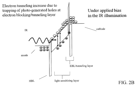
Figures 2A and 2B demonstrate the operating principle of a photodetector
according
to an embodiment of the subject invention. Referring to Figure 2A, when a bias
is applied in
the dark (i.e., no visible and/or IR light), holes are blocked from the first
electrode due to hole
blocking layer, and electrons are blocked from second electrode due to the
electron blocking
layer. Referring to Figure 2B, when the photodetector is irradiated with light
(e.g., IR light),
the light sensitizing layer (e.g., an IR sensitizing layer) generates electron-
hole pairs, and the
electrons flow to the first electrode due to the applied bias. The holes are
accumulated in
bulk trap sites of the electron blocking/tunneling layer, and the accumulated
holes reduce the
barrier width of the electron blocking/tunneling layer. Thus, the electron
tunneling from the
second electrode to the light sensitizing layer is enhanced significantly,
thus producing gain.
Figure 3A shows a schematic band diagram of a photodetector according to an
embodiment of subject invention, and Figure 3B shows the dark and photo
current density-
voltage (J-V) characteristics for a photodetector according to an embodiment
of the subject
invention.
Figure 4A shows a plot of the gain versus the applied voltage for a
photodetector
according to the subject invention, and Figure 4B shows a plot of the
detectivity versus the
SUBSTITUTE SHEET (RULE 26)
CA 02840498 2013-12-24
WO 2013/003850
PCT/US2012/045272
6
applied voltage for a photodetector according to an embodiment of the subject
invention.
Referring to Figure 4A, a very high gain can be seen, including a gain of more
than 150 at an
applied bias of -20 V. Referring to Figure 4B, the detectivity is saturated to
more than 5 x
1012 Jones at values of the applied voltage of less than -18 V.
According to embodiments of the subject invention, a photodetector exhibits
gain at
applied bias (i.e., it is a photodetector with gain). The photodetector can
exhibit a gain of, for
example, about 150 at an applied bias of -20 V. In various embodiments, the
photodetector
can exhibit a gain any of the following values or ranges: 2, about 2, at least
2, 3, about 3, at
least 3, ... , 160, about 160, at least 160 (where the "..." represents each
number between 3
and 160, "about" each number between 3 and 160, and "at least" each number
between 3 and
160), or any range having a first endpoint of any number from 2 to 159 and a
second endpoint
of any number from 3 to 160. The gain values and ranges of the preceding
sentence can be
exhibited at any applied voltage value from -30 V to 30 V.
Referring to Figures 5A-5C, embodiments of the subject invention also pertain
to an
IR-to-visible upconversion device 500. The IR-to-visible upconversion device
500 can
include a photodetector 10 and a light-emitting device (LED) 200. In many
embodiments,
the LED 200 can be an organic LED (OLED). The IR-to-visible upconversion
device 500
can be an IR-to-visible upconversion device with gain, and the photodetector
10 can be a
photodetector with gain. In specific embodiments, the IR-to-visible
upconversion device can
include a photodetector with gain, as illustrated in Figures 1A-1B, 2A-2B, 3A-
3B, and 4A-4B
and/or as described in connection with the photodetectors of Figures 1A-1B, 2A-
2B, 3A-3B,
and 4A-4B. The OLED 200 can include at least one electrode, a hole
transporting layer
(HTL), a light emitting layer (LEL), and an electron transporting layer (ETL).
At least one electrode of the OLED 200 can be transparent to at least a
portion of
visible light and/or at least a portion of IR light, though embodiments are
not limited thereto.
Each electrode of the OLED 200 can include one or more of the following
materials: ITO,
IZO, ATO, AZO, silver, calcium, magnesium, gold, aluminum, carbon nanotubes,
silver
nanowire, LiF/Al/ITO, Ag/ITO, CsCO3/ITO, and a Mg:Ag/A1q3 stack layer, though
embodiments are not limited thereto. The HTL of the OLED 200 can include one
or more of
the following materials: NPD, TAPC, TFB, TPD, and diamine derivative, though
embodiments are not limited thereto. The LEL of the OLED 200 can include one
or more of
the following materials: Iridium tris(2-phenylpyidine) (Ir(ppy)3), [2-methoxy-
5-(2-
ethylhexyloxy)-p-phenylenevinylene] (MEH-PPV), Tris-(8-quinolinolato)
aluminum) (Alq3),
SUBSTITUTE SHEET (RULE 26)
CA 02840498 2013-12-24
WO 2013/003850
PCT/US2012/045272
7
and bis[(4,6-di-fluoropheny1)-pyridinatedpicolinate (Flrpic), though
embodiments are not
limited thereto. The ETL of the OLED 200 can include one or more of the
following
materials: BCP, Bphen, 3TPYMB, and A1q3, though embodiments are not limited
thereto.
In a particular embodiment, the electrode of the OLED 200 is a Mg:Ag/A1q3
stack
layer. The Mg:Ag layer of the Mg:Ag/A1q3 stack layer can have a composition
of, for
example, Mg:Ag (10:1) and can have a thickness of, for example, less than
30nm. The A1q3
layer of the Mg:Ag/A1q3 stack layer can have a thickness of, for example, from
0 nm to 200
mm
The photodetector 10 can be a photodetector with gain as described herein,
though
only one electrode need be present. That is, the photodetector 10 can include
at least one
electrode, a light sensitizing layer, and an electron blocking/tunneling
layer. The
photodetector 10 can also optionally include a substrate and/or a hole
blocking layer.
The electrode can include one or more of the following materials: ITO, IZO,
ATO,
AZO, silver, calcium, magnesium, gold, aluminum, carbon nanotubes, silver
nanowire,
LiF/Al/ITO, Ag/ITO, and CsCO3/ITO.
In certain embodiments, the photodetector 10 can be an IR photodetector and
the light
sensitizing layer can be an IR sensitizing layer. The light sensitizing layer
can include, for
example, one or more of the following materials: PbS nanocrystals (quantum
dots), PbSe
nanocrystals (quantum dots), PCTDA, SnPc, SnPc:C60, A1PcC1, AlPeCl:C60, Ti0Pc,
Ti0Pc:C60, PbSe, PbS, InAs, InGaAs, Si, Ge, and GaAs.
In an embodiment, the electron blocking/tunneling layer can be a TAPC/Mo03
stack
layer. The TAPC layer can have a thickness of, for example, 0 rim to 100 nm.
The Mo03
layer can have a thickness of, for example, 0 nm to 100 nm.
In an embodiment, the photodetector can include a hole blocking layer, and the
hole
blocking layer can include one or more of the following materials: ZnO, NTCDA,
BCP,
UGH2, BPhen, A1q3, mCP, 3TPYMB, and TiO2.
Referring to Figure 5A, in a further embodiment, the IR-to-visible
upconversion
device 500 can also include an interconnecting part 100 between the
photodetector 10 and the
OLED 200. The interconnecting part 100 can be positioned such that the
electron
blocking/tunneling layer of the photodetector 10 is closer than the light
sensitizing layer is to
the interconnecting part 100, and the HTL of the OLED 200 is closer than the
ETL is to the
interconnecting part 100. The photodetector 10 can include an electrode under
the light
SUBSTITUTE SHEET (RULE 26)
CA 02840498 2013-12-24
WO 2013/003850
PCT/US2012/045272
8
sensitizing layer, and that electrode can be an anode. The OLED 200 can
include an
electrode on the ETL, and that electrode can be a cathode.
In an embodiment, the interconnecting part 100 can include an HBL 110 and an
EBL
120. The lowest unoccupied molecular orbital (LUMO) of the HBL 110 of the
interconnecting part 100 can be close to the highest occupied molecular
orbital (HOMO) of
the EBL 120 of the interconnecting part 100. Thus, when a bias is applied,
electrons and
holes can be generated in the interconnecting part 100. In an embodiment, the
LUMO of the
HBL 110 of the interconnecting part 100 and the HOMO of the EBL 120 of the
interconnecting part 100 can be no more than 1 eV apart. In a further
embodiment, the
LUMO of the IIBL 110 of the interconnecting part 100 and the HOMO of the EBL
120 of the
interconnecting part 100 can be no more than 0.5 eV apart. That is, the energy
difference
between the HOMO of the EBL 120 of the interconnecting part 100 and the LUMO
of the
HBL 110 of the interconnecting part 100 can be 0.5 eV or less. The
interconnecting part 100
can be positioned within the IR-to-visible upconversion device 500 such that
the HBL 120 of
the interconnecting part 100 can be adjacent to the photodetector 10 and the
EBL 120 of the
interconnecting part 100 can be adjacent to the OLED 200. In embodiment, the
photodetector 10 can include a second electrode 70 on its EBL/tunneling layer,
and the HBL
120 of the interconnecting part 100 can be in direct contact with the second
electrode 70 of
the photodetector 10. The second electrode 70 of the photodetector 10 can be a
cathode. The
second electrode 70 of the photodetector 10 can include one or more of the
following
materials: ITO, IZO, ATO, AZO, silver, calcium, magnesium, gold, aluminum,
carbon
nanotubes, silver nanowire, LiF/A1/ITO, Ag/ITO, and CsCO3/ITO.
In a particular
embodiment, the second electrode 70 of the photodetector 10 can be a silver
electrode.
Though the dotted line around the interconnecting part 100 in Figure 5A
extends beyond the
HBL 110 and the EBL 120, the interconnecting part does not necessarily include
any
additional components beyond the HBL 110 and the EBL 120. In certain
embodiments,
additional components may be present (e.g., one or more electrodes or
substrates).
Referring again to Figures 5B and 5C, in an embodiment, the IR-to-visible
upconversion device 500 does not include an interconnecting part 100, and the
photodetector
10 is positioned directly adjacent to the OLED 200. The OLED 200 can be
positioned such
that the ETL of the OLED 200 is closer to the light sensitizing layer of the
photodetector 10
than it is to the electron blocking/tunneling layer of the photodetector 10.
In a particular
embodiment, the photodetector can include a hole blocking layer adjacent to
the light
SUBSTITUTE SHEET (RULE 26)
CA 02840498 2013-12-24
WO 2013/003850
PCT/US2012/045272
9
sensitizing layer, and the ETL of the OLED 200 can be positioned adjacent to
and in contact
with the hole blocking layer of the photodetector 10. The photodetector 10 can
include an
electrode adjacent to and in contact with the electron blocking/tunneling
layer, and the OLED
200 can include an electrode adjacent to and in contact with the HTL. The
electrode of the
photodetector 10 can be, for example, a cathode, and the electrode of the OLED
200 can be,
for example, an anode.
In the IR-to-visible upconversion devices 500 shown in Figures 5A-5C, a
substrate
(not shown) can also be present. In many embodiments, the IR-to-visible
upconversion
device 500 can be flipped or turned around and still function properly. For
example, the
substrate can be adjacent to the anode in Figure 5B and adjacent to the
cathode in Figure 5C,
such that Figure 5B shows a similar configuration to that of Figure 5C but
with the IR-to-
visible upconversion device 500 turned around on the substrate. In the IR-to-
visible
upconversion device 500 depicted in Figure 5A, the substrate can be adjacent
to the anode or
the cathode. In a particular embodiment, an IR-to-visible upconversion device
500 can
include an interconnecting part 100 (as shown in Figure 5A), and the substrate
can be
adjacent to the anode. IR light can be incident on the IR-to-visible
upconversion device 500
from any direction, and visible light can be emitted from the IR-to-visible
upconversion
device 500 in any direction. The OLED 200 can be transparent to at least a
portion of light in
the IR spectrum, though embodiments are not limited thereto. The photodetector
10 can be
transparent to at least a portion of light in the visible spectrum, though
embodiments are not
limited thereto.
Referring again to Figures 5A-5C, the IR-to-visible upconversion device 500
functions by emitting visible light from the OLED 200 when the photodetector
10 absorbs IR
light. That is, the light sensitizing layer (e.g., an IR sensitizing layer) of
the photodetector 10
absorbs IR light, causing carriers to flow. The carriers flow to the OLED 200,
either directly
or via an interconnecting part 100, causing the LEL of the OLED 200 to emit
visible light.
The IR-to-visible upconversion device 500 can include a photodetector 10 with
gain and can
advantageously exhibit gain.
Embodiments of the subject invention also relate to methods of fabricating a
photodetector with gain. The photodetector can be, for example, an IR
photodetector. In an
embodiment, a method of fabricating a photodetector with gain can include:
forming a light
sensitizing layer on a first electrode, forming an electron blocking/tunneling
layer on the light
sensitizing layer, and forming a second electrode on the electron
blocking/tunneling layer.
SUBSTITUTE SHEET (RULE 26)
CA 02840498 2013-12-24
WO 2013/003850
PCT/US2012/045272
The method can also optionally include forming the first electrode on a
substrate and/or
conning a hole blocking layer on the first electrode such that the light
sensitizing layer is
formed on the hole blocking layer. The substrate can be, for example, a glass
substrate.
The first electrode can be a cathode, and the second electrode can be an
anode. In an
5
alternative embodiment, the first electrode can be an anode, and the second
electrode can be a
cathode. In certain embodiments, the first electrode and/or the second
electrode can be
transparent to at least a portion of visible and/or at least a portion of IR
light, though
embodiments are not limited thereto.
The first electrode can include one or more of the following materials: indium
tin
10
oxide (ITO), indium zinc oxide (IZO), aluminum tin oxide (ATO), aluminum zinc
oxide
(AZO), silver, calcium, magnesium, gold, aluminum, carbon nanotubes, silver
nanowire,
LiF/Al/ITO, Ag/ITO, and CsCO3/ITO. The second electrode can include one or
more of the
following materials: ITO, IZO, ATO, AZO, silver, calcium, magnesium, gold,
aluminum,
carbon nanotubes, silver nanowire, LiF/Al/ITO, Ag/ITO, and CsCO3/ITO.
In certain embodiments, the photodetector can be an IR photodetector and the
light
sensitizing layer can be an IR sensitizing layer. The light sensitizing layer
can include, for
example, one or more of the following materials: PbS nanocrystals (quantum
dots), PbSe
nanocrystals (quantum dots), PCTDA, SnPc, SnPc:C60, AlNCI, A1PcC1:C60, Ti0Pc,
Ti0Pc:C60, PbSe, PbS, InAs, InGaAs, Si, Ge, and GaAs.
In an embodiment, the electron blocking/tunneling layer can be a TAPC/Mo03
stack
layer. The TAPC layer can be formed to a thickness of, for example, 0 nm to
100 nm. The
Mo03 layer can be formed to a thickness of, for example, 0 nm to 100 nm.
In an embodiment, the method can include forming a hole blocking layer, and
the hole
blocking layer can include one or more of the following materials: ZnO, NTCDA,
BCP,
UGH2, BPhen, A1q3, 3mCP, 3TPYMB, and TiO2.
In a particular embodiment, the method of fabricating a photodetector can
include:
forming a light sensitizing layer on a first electrode, forming an electron
blocking/tunneling
layer on the light sensitizing layer, and forming a second electrode on the
electron
blocking/tunneling layer. The electron blocking/tunneling layer can be, for
example, a
TAPC/Mo03 stack layer, and the TAPC/Mo03 stack layer can be formed such that
the TAPC
layer is formed directly on and in contact with the light sensitizing layer
and the Mo03 layer
is formed directly on and in contact with the TAPC layer. The second electrode
can then be
formed directly on and in contact with the Mo03 layer of the TAPC/Mo03 stack
layer. The
SUBSTITUTE SHEET (RULE 26)
CA 02840498 2013-12-24
WO 2013/003850
PCT/US2012/045272
11
light sensitizing layer can be, for example, an IR sensitizing layer and can
include, e.g., PbS
quantum dots. In a further embodiment, the method can include forming a hole
blocking
layer on the first electrode such that the light sensitizing layer is formed
directly on and in
contact with the hole blocking layer.
Embodiments of the subject invention also relate to methods of detecting
radiation
using a photodetector with gain. The photodetector can be, for example, an IR
photodetector
such that the method can detect IR radiation. In an embodiment, a method of
using a
photodetector with gain to detect radiation can include: providing a
photodetector with gain,
wherein the photodetector includes a first electrode, a light sensitizing
layer, an electron
blocking/tunneling layer, and a second electrode. The photodetector can also
optionally
include a substrate and/or a hole blocking layer. The substrate can be, for
example, a glass
substrate.
The first electrode can be a cathode, and the second electrode can be an
anode. In an
alternative embodiment, the first electrode can be an anode, and the second
electrode can be a
cathode. In certain embodiments, the first electrode and/or the second
electrode can be a
transparent electrode.
The first electrode can include one or more of the following materials: indium
tin
oxide (ITO), indium zinc oxide (IZO), aluminum tin oxide (ATO), aluminum zinc
oxide
(AZO), silver, calcium, magnesium, gold, aluminum, carbon nanotubes, silver
nanowire,
LiF/Al/ITO, Ag/ITO, and CsCO3/ITO. The second electrode can include one or
more of the
following materials: ITO, IZO, ATO, AZO, silver, calcium, magnesium, gold,
aluminum,
carbon nanotubes, silver nanowire, LiF/AVITO, Ag/ITO, and CsCO3/ITO.
In certain embodiments, the photodetector can be an IR photodetector and the
light
sensitizing layer can be an IR sensitizing layer. The light sensitizing layer
can include, for
example, one or more of the following materials: PbS nanocrystals (quantum
dots), PbSe
nanocrystals (quantum dots), PCTDA, SnPc, SnPc:C60, A1PcC1, AlPcCl:C60, Ti0Pc,
Ti0Pc:C60, PbSe, PbS, InAs, InGaAs, Si, Ge, and GaAs.
In an embodiment, the electron blocking/tunneling layer can be a TAPC/Mo03
stack
layer. The TAPC layer can be formed to a thickness of, for example, 0 nm to
100 nm. The
Mo03 layer can be formed to a thickness of, for example, 0 nm to 100 nm.
In an embodiment, the photodetector can include a hole blocking layer, and the
hole
blocking layer can include one or more of the following materials: ZnO, NTCDA,
BCP,
UGH2, BPhen, Alq3, 3mCP, 3TPYMB, and Ti02.
SUBSTITUTE SHEET (RULE 26)
CA 02840498 2013-12-24
WO 2013/003850
PCT/US2012/045272
12
In a particular embodiment, the photodetector can include: a light sensitizing
layer on
a first electrode, an electron blocking/tunneling layer on the light
sensitizing layer, and a
second electrode on the electron blocking/tunneling layer. The electron
blocking/tunneling
layer can be, for example, a TAPC/Mo03 stack layer, and the TAPC/Mo03 stack
layer can be
positioned such that the TAPC layer is directly on and in contact with the
light sensitizing
layer and the Mo03 layer is directly on and in contact with the TAPC layer.
The second
electrode can then be directly on and in contact with the Mo03 layer of the
TAPC/Mo03
stack layer. The light sensitizing layer can be, for example, an IR
sensitizing layer and can
include, e.g., PbS quantum dots. In a further embodiment, the photodetector
can include a
hole blocking layer on the first electrode and under the light sensitizing
layer.
Embodiments of the subject invention also relate to methods of forming an IR-
to-
visible upconversion device. The IR-to-visible upconversion device can be an
IR-to-visible
upconversion device with gain, and the photodetector can be a photodetector
with gain. In an
embodiment, a method of fabricating an IR-to-visible upconversion device can
include:
forming a photodetector with gain; forming an LED; and coupling the LED and
the
photodetector with gain. The LED can be an OLED. Forming the OLED can include:
forming at least one electrode, forming a hole transporting layer (HTL),
forming a light
emitting layer (LEL), and forming an electron transporting layer (ETL).
At least one electrode of the OLED can be transparent to at least a portion of
visible
and/or at least a portion of IR light, though embodiments are not limited
thereto. Each
electrode of the OLED can include one or more of the following materials: ITO,
IZO, ATO,
AZO, silver, calcium, magnesium, gold, aluminum, carbon nanotubes, silver
nanowire,
LiF/Al/ITO, Ag/ITO, CsCO3/ITO, and a Mg:Ag/A1q3 stack layer, though
embodiments are
not limited thereto. The HTL of the OLED can include one or more of the
following
materials: NPD, TAPC, TFB, TPD, and diamine derivative, though embodiments are
not
limited thereto. The LEL of the OLED can include one or more of the following
materials:
Ir(ppy)3, MEH-PPV, A1q3, and Flrpic, though embodiments are not limited
thereto. The
ETL of the OLED can include one or more of the following materials: BCP,
Bphen,
3TPYMB, and Alq3, though embodiments are not limited thereto.
In a particular embodiment, the electrode of the OLED is a Mg:Ag/A1q3 stack
layer.
The Mg:Ag layer of the Mg:Ag/A1q3 stack layer can have a composition of, for
example,
Mg:Ag (10:1) and can be formed to a thickness of, for example, less than 30nm.
The A1q3
SUBSTITUTE SHEET (RULE 26)
CA 02840498 2013-12-24
WO 2013/003850
PCT/US2012/045272
13
layer of the Mg:Ag/A1q3 stack layer can be formed to a thickness of, for
example, from 0 nm
to 200 nm.
The photodetector can be a photodetector with gain and can be formed as
described
herein, though only one electrode need be formed. That is, forming the
photodetector can
include forming at least one electrode, forming a light sensitizing layer, and
forming an
electron blocking/tunneling layer. Forming the photodetector can also
optionally include
proving a substrate and/or forming a hole blocking layer.
The electrode can be formed of one or more of the following materials: ITO,
IZO,
ATO, AZO, silver, calcium, magnesium, gold, aluminum, carbon nanotubes, silver
nanowire,
LiF/AUITO, Ag/ITO, and CsCO3/ITO.
In certain embodiments, the photodetector can be an IR photodetector and the
light
sensitizing layer can be an IR sensitizing layer. The light sensitizing layer
can be formed of,
for example, one or more of the following materials: PbS nanocrystals (quantum
dots), PbSe
nanocrystals (quantum dots), PCTDA, SnPc, SnPc:C60, AlPcCI, A1PeC1:C60, Ti0Pc,
Ti0Pc:C60, PbSe, PbS, InAs, InGaAs, Si, Ge, and GaAs.
In an embodiment, the electron blocking/tunneling layer can be a TAPC/Mo03
stack
layer. The TAPC layer can be formed to a thickness of, for example, 0 nm to
100 mu. The
Mo03 layer can be formed to a thickness of, for example, 0 nm to 100 nm.
In an embodiment, forming the photodetector can include forming a hole
blocking
layer, and the hole blocking layer can include one or more of the following
materials: ZnO,
NTCDA, BCP, UGH2, BPhen, Alq3, mCP, 3TPYMB, and TiO2.
In a further embodiment, coupling the photodetector with gain to the OLED can
include coupling the photodetector with gain to an interconnecting part and
coupling the
OLED to the interconnecting part. The photodetector can be coupled to the
interconnecting
part such that the electron blocking/tunneling layer of the photodetector is
closer than the
light sensitizing layer is to the interconnecting part. The OLED can be
coupled to the
interconnecting part such that the HTL of the OLED is closer than the ETL is
to the
interconnecting part. The photodetector can include an electrode under the
light sensitizing
layer, and that electrode can be an anode. The OLED can include an electrode
on the ETL,
and that electrode can be a cathode.
In an embodiment, coupling the photodetector with gain to the OLED can include
coupling the photodetector with gain directly to the OLED. The photodetector
with gain can
be coupled to the OLED such that the ETL of the OLED is closer to the light
sensitizing layer
SUBSTITUTE SHEET (RULE 26)
CA 02840498 2013-12-24
WO 2013/003850
PCT/US2012/045272
14
of the photodetector than it is to the electron blocking/tunneling layer of
the photodetector.
In a particular embodiment, the photodetector can include a hole blocking
layer adjacent to
the light sensitizing layer, and the photodetector with gain can be coupled to
the OLED such
that the ETL of the OLED is adjacent to and in contact with the hole blocking
layer of the
photodetector. The photodetector can include an electrode adjacent to and in
contact with the
electron blocking/tunneling layer, and the OLED can include an electrode
adjacent to and in
contact with the HTL. The electrode of the photodetector can be, for example,
a cathode, and
the electrode of the OLED can be, for example, an anode.
Embodiments of the subject invention also relate to methods of upconverting IR
radiation to visible radiation using an IR-to-visible upconversion device. The
IR-to-visible
upconversion device can include a photodetector and an LED. The LED can be an
OLED.
The IR-to-visible upconversion device can be an IR-to-visible upconversion
device with gain,
and the photodetector can be a photodetector with gain. The OLED can include
at least one
electrode, a hole transporting layer (HTL), a light emitting layer (LEL), and
an electron
transporting layer (ETL).
At least one electrode of the OLED can be transparent to at least a portion of
visible
and/or at least a portion of IR light, though embodiments are not limited
thereto. Each
electrode of the OLED can include one or more of the following materials: ITO,
IZO, ATO,
AZO, silver, calcium, magnesium, gold, aluminum, carbon nanotubes, silver
nanowire,
LiF/Al/ITO, Ag/ITO, CsCO3/ITO, and a Mg:Ag/A1q3 stack layer, though
embodiments are
not limited thereto. The HTL of the OLED can include one or more of the
following
materials: NPD, TAPC, TFB, TPD, and diamine derivative, though embodiments are
not
limited thereto. The LEL of the OLED can include one or more of the following
materials:
Ir(ppy)3, MEH-PPV, Alq3, and Flrpic, though embodiments are not limited
thereto. The
ETL of the OLED can include one or more of the following materials: BCP,
Bphen,
3TPYMB, and A1q3, though embodiments are not limited thereto.
In a particular embodiment, the electrode of the OLED is a Mg:Ag/A1q3 stack
layer.
The Mg:Ag layer of the Mg:Ag/A1q3 stack layer can have a composition of, for
example,
Mg:Ag (10:1) and can have a thickness of, for example, less than 30nm. The
Alq3 layer of
the Mg:Ag/A1q3 stack layer can have a thickness of, for example, from 0 nm to
200 run.
The photodetector can be a photodetector with gain as described herein, though
only
one electrode need be present. That is, the photodetector can include at least
one electrode, a
SUBSTITUTE SHEET (RULE 26)
CA 02840498 2013-12-24
WO 2013/003850
PCT/US2012/045272
light sensitizing layer, and an electron blocking/tunneling layer. The
photodetector can also
optionally include a substrate and/or a hole blocking layer.
The electrode can include one or more of the following materials: ITO, IZO,
ATO,
AZO, silver, calcium, magnesium, gold, aluminum, carbon nanotubes, silver
nanowire,
5 LiF/AUITO, Ag/ITO, and CsCO3/ITO.
In certain embodiments, the photodetector can be an IR photodetector and the
light
sensitizing layer can be an IR sensitizing layer. The light sensitizing layer
can include, for
example, one or more of the following materials: PbS nanocrystals (quantum
dots), PbSe
nanocrystals (quantum dots), PCTDA, SnPc, SnPc:C60, AlPeCl, A1PeC1:C60, Ti0Pc,
10 Ti0Pc:C60, PbSe, PbS, InAs, InGaAs, Si, Ge, and GaAs.
In an embodiment, the electron blocking/tunneling layer can be a TAPC/Mo03
stack
layer. The TAPC layer can have a thickness of, for example, 0 mu to 100 nm.
The Mo03
layer can have a thickness of, for example, 0 nm to 100 nm.
In an embodiment, the photodetector can include a hole blocking layer, and the
hole
15 blocking layer can include one or more of the following materials: ZnO,
NTCDA, BCP,
UGH2, BPhen, A1q3, mCP, 3TPYMB, and TiO2.
In a further embodiment, the IR-to-visible upconversion device can also
include an
interconnecting part between the photodetector and the OLED. The
interconnecting part can
be positioned such that the electron blocking/tunneling layer of the
photodetector is closer
than the light sensitizing layer is to the interconnecting part, and the HTL
of the OLED is
closer than the ETL is to the interconnecting part. The photodetector can
include an electrode
under the light sensitizing layer, and that electrode can be an anode. The
OLED can include
an electrode on the ETL, and that electrode can be a cathode.
In an embodiment, the IR-to-visible upconversion device does not include an
interconnecting part, and the photodetector is positioned directly adjacent to
the OLED. The
OLED can be positioned such that the ETL of the OLED is closer to the light
sensitizing
layer of the photodetector than it is to the electron blocking/tunneling layer
of the
photodetector. In a particular embodiment, the photodetector can include a
hole blocking
layer adjacent to the light sensitizing layer, and the ETL of the OLED can be
positioned
adjacent to and in contact with the hole blocking layer of the photodetector.
The
photodetector can include an electrode adjacent to and in contact with the
electron
blocking/tunneling layer, and the OLED can include an electrode adjacent to
and in contact
SUBSTITUTE SHEET (RULE 26)
CA 02840498 2013-12-24
WO 2013/003850
PCT/US2012/045272
16
with the HTL. The electrode of the photodetector can be, for example, a
cathode, and the
electrode of the OLED can be, for example, an anode.
In many embodiments, the IR-to-visible upconversion device can be flipped or
turned
around and still function properly. The OLED can be transparent to at least a
portion of light
in the IR spectrum, though embodiments are not limited thereto. The
photodetector can be
transparent to at least a portion of light in the visible spectrum, though
embodiments are not
limited thereto.
The IR-to-visible upconversion device upconverts IR light to visible light.
The IR-to-
visible upconversion emits visible light from the OLED when the photodetector
absorbs IR
light. That is, the light sensitizing layer (e.g., an IR sensitizing layer) of
the photodetector
absorbs IR light, causing carriers to flow. The carriers flow to the OLED,
either directly or
via an interconnecting part, causing the LEL of the OLED to emit visible
light. The IR-to-
visible upconversion device can include a photodetector with gain and can
advantageously
exhibit gain.
EXAMPLE 1
A photodetector was fabricated on a glass substrate. The photodetector
included an
ITO first electrode, a ZnO hole blocking layer on the first electrode, a PbS
quantum dot light
sensitizing layer on the hole blocking layer, a TAPC/Mo03 stack electron
blocking/tunneling
layer on the light sensitizing layer, and a second electrode on the electron
blocking/tunneling
layer. The PbS quantum dot light sensitizing layer had the absorbance spectrum
shown in
Figure 1A. The photodetector displayed the J-V characteristic curves (for dark
and IR
illumination at 1240 nm and 0.302 W/cm2) shown in Figure 3B. Additionally, the
photodetector exhibited the gain and detectivity, as functions of applied
voltage, shown in
Figures 4A and 4B, respectively.
All patents, patent applications, provisional applications, and publications
referred to
or cited herein are incorporated by reference in their entirety, including all
figures and tables,
to the extent they are not inconsistent with the explicit teachings of this
specification.
It should be understood that the examples and embodiments described herein are
for
illustrative purposes only and that various modifications or changes in light
thereof will be
suggested to persons skilled in the art and are to be included within the
spirit and purview of
this application.
SUBSTITUTE SHEET (RULE 26)