Note: Descriptions are shown in the official language in which they were submitted.
CA 02840720 2013-12-30
1
PCT/JP2011/071131
HIGH-PURITY YTTRIUM, PROCESS OF PRODUCING HIGH-PURITY YTTRIUM,
HIGH-PURITY YTTRIUM SPUTTERING TARGET, METAL GATE FILM DEPOSITED
WITH HIGH-PURITY YTTRIUM SPUTTERING TARGET, AND SEMICONDUCTOR
ELEMENT AND DEVICE EQUIPPED WITH THE METAL GATE FILM
TECHNICAL FIELD
[0001]
The present invention relates to high-purity yttrium, a method of producing
the high-purity yttrium, a sputtering target produced using the high-purity
yttrium,
a metal gate film mainly composed of the high-purity yttrium, and a
semiconductor element and a device each comprising the metal gate film.
BACKGROUND ART
[0002] Yttrium
(Y) is a rare earth element. Yttrium is an ash black metal having
an atomic number of 39 and an atomic weight of 88.91 and has a hexagonal
close-packed structure, a melting point of 1520 C, a boiling point of 3300 C,
and a density of 4.47 g/cm3. Yttrium is readily oxidized on the surface in the
air, is soluble in acid, but insoluble in alkali, and reacts with hot water.
Its
ductility and extensibility are low (see Dictionary of Physics and Chemistry).
[0003] Rare earth elements having an oxidation number of 3 are
generally stable,
and yttrium is trivalent. Recently, yttrium has been researched and developed
as an electronic material such as a metal gate material or a high-dielectric
constant (high-k) material and is a metal attracting a lot of attention.
An yttrium metal has a problem of being easily oxidized during purification
and is therefore a material of which high-purification is difficult and there
was
not a high-purity product. An yttrium metal that has been left to stand in the
air
is oxidized within a short period of time into Y203 and changes the color into
black.
Recently, there is a demand for reducing the thicknesses of gate insulating
films of next-generation MOSFETs, but in Si02, which has been used for gate
insulating films, the leak current due to a tunnel effect increases with a
reduction in thickness, resulting in a difficulty in normal operation.
[0004]
Accordingly, as alternatives thereto, Hf02, Zr02, A1203, and La203 have
been proposed as materials having high dielectric constants, high thermal
CA 02840720 2013-12-30
2
PCT/JP2011/071131
stability, and high energy barriers to holes and electrons in silicon. In
these
materials, in particular, La203 is highly rated and has been investigated for
its
electrical characteristics, and studies on La203 as a material for gate
insulating
films in next-generation MOSFETs have been reported (see Non-Patent
Document 1). However, the study in this Non-Patent Document relates to
La203 films and does not particularly mention the characteristics and
behaviors
of an yttrium (Y) element itself.
[0005] Thus, lanthanum is a material that is gathering attention in a
tendency of
recent technologies, but yttrium, which is a metal having similar physical
properties as a rare earth metal, has almost not been studied for its use as
an
electronic part material. It is easily supposed that if yttrium is used in
such an
electronic part (e.g., a gate insulating film of next-generation MOSFET), the
presence of other impurities is undesirable for taking advantage of the
characteristics of yttrium itself as a metal having physical properties as a
rare
earth metal, and an increase in purity is necessary.
[0006] Thus, yttrium (yttrium oxide) is still in the research phase. In
investigation
of the characteristics of yttrium (yttrium oxide), if an yttrium metal itself
is
present as a sputtering target material, the sputtering target has such
considerable advantages that: a thin film of yttrium can be formed on a
substrate; the behaviors of the interface with a silicon substrate can be
readily
investigated; the characteristics of, for example, a gate insulating film
having a
high dielectric constant can be readily investigated by forming an yttrium
compound; and also the degree of freedom as a product increases.
[0007] In
formation of a film by sputtering with a target of yttrium, occurrence of a
protrusion (nodule) on a target surface is a problem. The protrusion induces
abnormal discharge to cause generation of particles by, for example, rupture
of
the protrusion (nodule).
The generation of particles causes increases in failure rates of metal gate
films and semiconductor elements and devices. Accordingly, in order to utilize
the characteristics of yttrium, reductions in contents of, in particular, Al,
Fe, and
Cu are required. In addition, carbon (graphite) contained in yttrium is
present
as a solid and is difficult to be detected because of it conductivity. The
amount
of carbon is therefore required to be reduced.
[0008]
Furthermore, yttrium is a material of which high purification is difficult,
but in
order to utilize the characteristics of yttrium, in addition to Al, Fe, Cu,
and
CA 02840720 2013-12-30
3
PCT/JP2011/071131
carbon (graphite), the amounts of materials that affect the characteristics of
semiconductors, such as alkaline metals, alkali earth metals, transition metal
elements, high-melting-point metal elements, and radioactive elements, are
required to be reduced. Accordingly, yttrium is desired to have a purity of 5N
or more.
[0009]
Furthermore, there is a problem that removal of lanthanoids other than
yttrium is significantly difficult.
Fortunately, since lanthanoids other than
yttrium have similar properties, slight contamination thereof does not cause
any
problem. In addition, slight contamination of gas components does not cause
a big problem. Removal of gas components is usually difficult, and purities
are
generally shown as those excluding gas components.
[0010] Conventionally, the problems related to characteristics of
yttrium, how to
produce high-purity yttrium, and behaviors of impurities contained in an
yttrium
target have not sufficiently investigated.
Accordingly, it is desired to
immediately solve the problems mentioned above.
[0011] In publicly known documents, Patent Document 1 describes a
molten salt
electrolysis apparatus that can be installed to a vacuum distillation
apparatus as
an apparatus for producing high-purity yttrium. In this case, however, it is
unclear how highly purified yttrium can be produced.
Patent Document 2 discloses, as a method of producing high-purity yttrium,
a method in which machinery arrangement of a molten salt electrolysis
apparatus and a vacuum distillation apparatus has been devised, and proposes
subjecting the high-purity yttrium to electron beam melting thereafter. In
addition, an example of reducing each concentration of Fe, Cr, Ni, U, and Th
as
impurities of interest to less than 1 ppm is shown. However, it is not clearly
described how much the impurities can be reduced in each step, what becomes
of other impurities, and how much high purity is eventually achieved.
[0012] Patent Document 3 describes a molten salt electrolysis apparatus
in which
the structure of a crucible has been devised for a method of producing
high-purity yttrium. In addition,
an example of yttrium in which each
concentration of Fe, Cr, Ni, Cu, U, and Th as impurities of interest is
reduced to
less than 1 ppm is shown. However, it is unclear how highly purified yttrium
can be produced and how impurities other than the above are removed from
yttrium.
[0013] Patent Document 4 describes a molten salt electrolysis apparatus in
which
CA 02840720 2013-12-30
. ' 4
PCT/JP2011/071131
,
the structures of an anode and a crucible have been devised for a method of
producing high-purity yttrium. In addition, an example of yttrium in which
each
concentration of Fe, Cr, Ni, Cu, U, and Th as impurities of interest is
reduced to
less than 1 ppm is shown. However, it is unclear how highly purified yttrium
can be produced and how impurities other than the above are removed from
yttrium.
[0014] Patent
Document 5 describes a vacuum distillation apparatus for yttrium
chloride anhydrous in which the arrangement structure of a distillation
container
and a condenser is devised for a method of producing high-purity yttrium. In
addition, an example of yttrium in which each concentration of Fe, Cr, Ni, Cu,
Mg, and Mn as impurities of interest is reduced to less than 1 ppm is shown.
However, it is unclear how highly purified yttrium can be eventually produced
and how impurities other than the above are removed from yttrium.
[0015] Patent
Document 6 describes use of an amorphous film of yttrium for
forming a YAG thin film that is used as a solid laser oscillation material.
High-purity yttrium is probably used, but the purity of this yttrium and the
technology for producing this high-purity yttrium are not disclosed.
Patent Document 7 describes a solvent extraction process as a method of
separating high-purity yttrium. It is described that the resulting purity of a
Y
compound relative to all rare earth compounds reaches 99.0% to 99.996%
(wt%). However, it is not clearly described what becomes of other impurities
such as transition metals and how much high purity is achieved on the whole.
[0016] Patent Document 1: Japanese Patent Laid-Open No. H04-176886
Patent Document 2: Japanese Patent Laid-Open No. H04-176887
Patent Document 3: Japanese Patent Laid-Open No. H04-176888
Patent Document 4: Japanese Patent Laid-Open No. H04-176889
Patent Document 5: Japanese Patent Laid-Open No. H05-17134
Patent Document 6: Japanese Patent Laid-Open No. H07-126834
Patent Document 7: Japanese Patent Laid-Open No. 2004-36003
[0017] Non-Patent Document 1: Eisuke Tokumitsu and two others, "Study of oxide
materials for high-k gate insulating film", Denki Gakkai Denshi Zairyo
Kenkyukai Shiryo, Vol. 6-13, pp. 37-41, published on 21 September, 2001
SUMMARY OF INVENTION
CA 02840720 2017-01-06
52898-13
[Technical Problem]
[0018] It is an object of the present invention to provide a method of
producing
high-purity yttrium, high-purity yttrium, a sputtering target produced using
the high-
purity yttrium, a metal gate film formed using the sputtering target, and a
technology
5 capable of stably providing a semiconductor element and a device each
comprising
the metal gate film.
[Solution to Problem]
[0019] The present invention provides high-purity yttrium and a high-
purity
yttrium sputtering target each having a purity, excluding rare earth elements
and gas
components, of 5N or more and containing 1 wt ppm or less of each of Al, Fe,
and
Cu. The high-purity yttrium may be high-purity cast yttrium.
The present invention also provides the high-purity yttrium and the high-
purity yttrium sputtering target according to the above, wherein the total
amount of W,
Mo, and Ta is 10 wt ppm or less; the amount of each of U and Th is 50 wt ppb
or
less; and the amount of carbon is 150 wt ppm or less. The invention also
provides
high-purity yttrium and a high-purity yttrium sputtering target each having a
purity,
excluding rare earth elements and gas components, of 5N or more and containing
10 wt ppm or less of the total amount of Al, Fe, Cu, W, Mo, Ta, U, Th, and
carbon.
In the high-purity yttrium and the high-purity yttrium sputtering target,
the radiation dose (a-ray dose) is less than 0.001 cph/cm2.
[0020] Regarding the production of the high-purity yttrium and the
high-purity
yttrium target, the invention can provide a method of producing the high-
purity yttrium
as described herein, by molten salt electrolysis of a raw material being a
crude
yttrium oxide having a purity, excluding gas components, of 4N or less at a
bath
temperature of 500 C to 800 C to obtain yttrium crystals; desalting treatment,
water
washing, and drying of the yttrium crystals; and electron beam melting for
removing
81775940
5a
volatile materials to achieve a purity, excluding rare earth elements and gas
components, of 5N or more.
As a molten salt electrolytic bath, potassium chloride (KCI), lithium
chloride (LiCI), and yttrium chloride (YCI3) are used. In the molten salt
electrolysis, an
anode made of Ta or stainless steel (SUS) can be used. The desalting treatment
can
be effectively performed by separating the metal and the salt from each other:
by
means of a vapor pressure differential by vacuum heating in a heating furnace
at a
temperature of 1000 C or less; or by dissolving the salt with an acid.
Thus, the present invention further provides a method for producing
high-purity cast yttrium having a purity, excluding rare earth elements and
gas
components, of 5N or more; containing 1 wt ppm or less of each of Al, Fe, and
Cu; 10
wt ppm or less of the total amount of W, Mo, and Ta; 50 wt ppb or less of each
of U
and Th; and 150 wt ppm or less of carbon, the method comprising: conducting
molten
salt electrolysis on a raw material, the raw material being a crude yttrium
oxide
having a purity, excluding gas components, of 4N or less, using an anode made
of
ferritic stainless steel (SUS), at a bath temperature of 500 C to 800 C to
obtain
yttrium crystals; desalting, water washing, and drying the yttrium crystals;
and
electron beam melting the yttrium crystals to remove volatile materials to
achieve a
purity, excluding rare earth elements and gas components, of 5N or more.
CA 2840720 2017-10-02
CA 02840720 2013-12-30
6
PCT/JP2011/071131
[0021] As
described above, it is possible to obtain high-purity yttrium and a
high-purity yttrium sputtering target each having a purity, excluding rare
earth
elements and gas components, of 5N (99.999 wt%) or more, wherein each
amount of aluminum (Al), iron (Fe), and copper (Cu) is 1 wt ppm or less, the
total amount of W, Mo, and Ta is 10 wt ppm or less, each amount of U and Th is
50 wt ppb or less, and the amount of carbon is 150 wt ppm or less.
In order to produce the high-purity yttrium having a purity, excluding rare
earth elements and gas components, of 5N or more, the steps and
manufacturing conditions in each step are important. The object of the
present invention cannot be achieved under conditions departing from such
conditions.
[0022] The high-purity yttrium prepared by the method described above
is a novel
material and is encompassed in the present invention. In a case of using
yttrium for the gate insulating film of an MOSFET, a YOx film is usually
formed.
In formation of such a film, an yttrium metal having high purity is necessary
for
increasing the degree of freedom in film formation to form an arbitrary film.
The present invention can provide a material satisfying this.
[0023] The rare earth elements contained in yttrium include, other than
yttrium(Y),
La, Sc, Y, Ce, Pr, Nd, Pm, Sm, Eu, Gd, Tb, Dy, Ho, Er, Tm, Yb, and Lu. These
elements have similar characteristics to those of Y, and it is therefore
difficult to
isolate and purify Y from these elements.
However, since these rare earth elements have approximate properties,
these rare earth elements do not particularly cause a problem in use of
yttrium
as an electronic part material as long as the total amount of these rare earth
elements is less than 100 wt ppm. Accordingly, the yttrium of the present
invention may contain the rare earth elements within the range above.
[0024] In general, gas components are C, N, 0, S, and H. Each of these
elements may be present as a single element or may be present in a form of a
compound (e.g., CO, CO2, or SO2) or a compound with a constituent element.
Since these gas component elements have low atomic weights and small
atomic radii, even if these elements are present as impurities of a material,
these gas component elements hardly affect the characteristics of the material
as long as the amount is not high. Accordingly, purities are generally shown
as those excluding gas components. In this sense, the purity of yttrium of the
present invention is 5N or more as a purity excluding gas components.
CA 02840720 2013-12-30
7
PCT/JP2011/071131
[0025] As
described above, the present invention provides high-purity yttrium
wherein the total amount of W, Mo, and Ta is 10 wt ppm or less; the amount of
each of U and Th is 50 wt ppb or less; and the amount of carbon is 150 wt ppm
or less. Furthermore, the total amount of aluminum (Al), iron (Fe), and copper
(Cu) is preferably 10 wt ppm or less. Since these elements are impurities that
reduce semiconductor characteristics, it is desirable to reduce the amounts of
these elements as much as possible.
[0026] The present invention can provide a sputtering target produced
using the
high-purity yttrium, a metal gate film formed using the sputtering target, and
a
semiconductor element and a device each comprising the metal gate film.
In a case of using yttrium for the gate insulating film of an MOSFET, as
described above, a YOx film is usually formed. In formation of such a film, an
yttrium metal having high purity is necessary for increasing the degree of
freedom in film formation to form an arbitrary film. The present invention can
provide a material satisfying this. Accordingly, the present invention
encompasses an appropriate combination of the high-purity yttrium with
another material in production of a target.
[0027] The high-purity yttrium prepared above is molten in vacuum and
is then
solidified into an ingot. This ingot is further cut into a predetermined size
and
polished to give high-purity yttrium or a high-purity yttrium sputtering
target.
As a result, high-purity yttrium and a high-purity yttrium sputtering target
each having a purity, excluding rare earth elements and gas components, of 5N
or more and containing 1 wt ppm or less of each of Al, Fe, and Cu can be
produced.
Furthermore, the radiation doses (a-ray doses) of the high-purity yttrium
and the high-purity yttrium sputtering target of the present invention can
each
achieve less than 0.001 cph/cm2.
[0028] Furthermore, sputtering of the target can give a metal gate film
having a
purity reflecting that of the target and having the same components as that of
the target. The sputtering target, the metal gate film, and a semiconductor
element and a device each comprising the film are all novel matters and are
encompassed in the present invention.
ADVANTAGEOUS EFFECTS OF INVENTION
CA 02840720 2013-12-30
8
PCT/JP2011/071131
[0029]
The present invention has an excellent effect capable of stably providing
high-purity yttrium, a sputtering target produced using the high-purity
yttrium, a
metal gate film formed using the sputtering target, and a semiconductor
element and a device each comprising the metal gate film.
BRIEF DESCRIPTION OF DRAWINGS
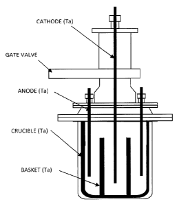
[0030] [Fig. 1] This is a diagram illustrating an example of the molten salt
electrolysis
apparatus.
[Fig. 2] This is a photograph showing an electrolytic deposit after molten
salt
electrolysis shown in Example 1.
DESCRIPTION OF EMBODIMENTS
[0031] The
present invention can use a crude yttrium oxide having a purity,
excluding gas components, of 4N or less as the yttrium raw material to be
highly purified.
Main impurities contained in such a material are, for example, Li, Na, K, Ca,
Mg, Al, Si, Ti, Fe, Cr, Ni, Mn, Mo, Ce, Pr, Nd, Sm, Ta, W, and gas components
(e.g., N, 0, C, and H).
[0032] Aluminum (Al) and copper (Cu), which are contained in yttrium
materials,
are widely used as alloy materials for substrates, sources, drains, and other
components of semiconductors and cause malfunction if they are contained in
a gate material even if it in a small amount. Iron (Fe), which is contained in
yttrium materials, is apt to be oxidized and causes sputtering failures when a
target includes iron. Furthermore, even if iron is not oxidized in a target,
oxidation after sputtering causes an increase in volume, which tends to cause
defects such as insulation failure. Therefore, iron is particularly
troublesome
because of causing operation failure and is required to be reduced.
[0033] Raw
materials contain large amounts of Fe and Al. Contamination with
Cu often occurs from water-cooling members that are used in production of
crude metals from chloride or fluoride by reduction. These impurity elements
are present in forms of oxides in many yttrium raw materials.
[0034]
The yttrium raw materials are usually prepared by calcium reduction of
yttrium fluoride or yttrium oxide, and the reducing agent composed of calcium
CA 02840720 2013-12-30
9
PCT/JP2011/071131
contains Fe, Al, and Cu as impurities. Consequently, impurity incorporation
from the calcium reducing agent into the yttrium raw materials often occurs.
(Molten salt electrolysis)
[0035] In
the present invention, in order to increase the purity of yttrium to achieve
a purity of 5N or more, molten salt electrolysis is performed. Fig. 1 shows an
example of a molten salt electrolysis apparatus. As shown in Fig. 1, an anode
made of Ta or ferritic stainless steel (SUS) is disposed at the lower part of
the
apparatus. Austenitic stainless steel containing Ni causes contamination with
Ni and is therefore improper.
[0036] Ta is used as a cathode. The portions that come into contact with
electrolytic bath/electrolytic deposit are all desirably made of Ta or
ferritic
stainless steel (SUS) for preventing contamination.
In particular, SUS is inexpensive and is therefore more preferred. Other
metals such as Ti and Ni that are used in molten salt electrolysis are apt to
form
alloys with Y and are therefore improper. Graphite is usually used in molten
salt electrolysis of rare earth elements, but graphite causes contamination
with
carbon. Accordingly, use of graphite must be avoided in the present invention.
In molten salt electrolysis, a crucible made of Ta or ferritic stainless steel
(SUS)
is used for avoiding contamination.
A basket for separating the Y raw material from the electrolytic deposit is
disposed at the central lower part. The upper half is a cooling tower. This
cooling tower is partitioned from the electrolytic bath with a gate valve
(GV).
[0037] The composition of a bath can be prepared by selecting one or
more from
potassium chloride (KCI), lithium chloride (LiCI), sodium chloride (NaCI),
magnesium chloride (MgC12), and calcium chloride (CaCl2) and mixing the
selected chloride(s) with yttrium chloride (YCI3). Another Y raw material can
also be used. The ratio of these materials is appropriately adjusted.
The yttrium raw material is desirably controlled to be 20% to 30% based on
the total weight of the salts. By doing so, efficient molten salt electrolysis
is
possible. The ratio of a salt is preferably determined as a point on a phase
diagram at which a minimum melting point occurs.
[0038] The temperature of the electrolytic bath is preferably adjusted
to be within a
range of 500 C to 800 C. The bath temperature does not highly affect
electrolysis, but a temperature higher than this range causes strong
volatilization of the salt constituting the bath to contaminate the gate valve
and
CA 02840720 2013-12-30
PCT/JP2011/071131
the cooling tower. Such a high temperature therefore makes cleaning thereof
complicated and therefore should be avoided.
A lower temperature makes handling easy. However, a temperature of
lower than the range decreases the fluidity of the bath to generate
distribution in
5 the
composition of the bath. As a result, normal electrodeposition tends not to
be achieved. The above-mentioned temperature range is therefore preferred.
[0039]
The atmosphere is an inert atmosphere. Electrolysis is generally carried
out under an Ar gas flow. The anode is preferably made of a material that
does not cause contamination. In such a sense, use of Ta or stainless steel
10 (SUS)
is desirable. The cathode is made of Ta. Though graphite is usually
used in molten salt electrolysis of rare earth elements, graphite causes
contamination with carbon. Accordingly, use of graphite must be avoided in
the present invention.
(Electrolysis condition)
[0040] The current density can be appropriately determined within a range
of 0.5
to 2.0 A/cm2. The voltage is about 0.5 to 1.0 V. These conditions are,
however, changed depending on the scale of the apparatus, and other
conditions are also acceptable. The electrolysis is usually carried out for
about 4 to 24 h. The weight of resultant electrolytic deposit is about 300 to
1000 g when the above-described molten salt electrolysis apparatus is used.
(Heating furnace)
[0041]
The metal and the salt are separated from each other by means of a vapor
pressure differential by vacuum heating in a heating furnace. The temperature
for desalting is usually 1000 C or less. The retention time is 10 to 200 h and
may be appropriately controlled based on the amount of raw materials. The
weight of electrolytic deposit Y is decreased by about 5% to 35% by the
desalting.
That is, it is demonstrated that desalting decreases the amount of Cl by
about 5% to 35%. The content of chlorine (Cl) contained in the Y material
after
desalting treatment is 50 to 3000 wt ppm.
(Induction melting)
[0042]
The resulting yttrium is subjected to induction melting in a vacuum
atmosphere using a water-cooled Cu crucible and is solidified into an ingot.
Though a water-cooled Cu crucible is used in this embodiment, a carbon
crucible can also be used depending on the melting apparatus. In this
CA 02840720 2013-12-30
11
PCT/JP2011/071131
,
induction melting, the amounts of Mg and Ca, which are difficult to be removed
by the molten salt electrolysis, can be removed.
(Electron beam melting)
[0043]
Electron beam melting of the resulting yttrium is performed by extensively
irradiating the molten yttrium raw material in the furnace with low-output
electron beams, usually, at 20 to 50 kW. This electron beam melting can be
repeated several times (2 to 4 times). An increase in the frequency of the
electron beam melting enhances the removal of volatile components such as Cl,
Ca, and Mg.
[0044] The induction melting and the electron beam melting may be performed
both or either one. In a case of performing both melting processes, the order
thereof is not particularly limited. The crucible used for melting may be made
of any material, and a water-cooled crucible is usually used.
[0045] In
the above, rare earth elements are excluded from impurities related to
the purity of high-purity yttrium. The reasons of this are as follows: since
rare
earth elements other than yttrium have chemical characteristics similar to
those
of yttrium, it is technically very difficult to remove such elements in
production of
high-purity yttrium, and also due to this similarity of the characteristics,
contamination with these elements as impurities does not cause a large
modification of the characteristics.
[0046] Because of such circumstances, contamination with rare earth
elements
other than yttrium is acceptable to some degree, but lower amounts of the rare
earth elements are desirable for enhancing the characteristics of yttrium
itself.
The purity, excluding gas components, is 5N or more. The reasons for
excluding gas components from impurities are as follows: it is difficult to
remove
gas components, and the amount of gas components does not become a
measure of improvement in purity. In general, presence of a small amount of
gas components is harmless compared to other impurity elements, in most
cases.
[0047] A thin film of an electronic material, such as a gate insulating
film or a
metal-gate thin film, is formed by sputtering in most cases, and sputtering is
an
excellent method for forming thin films. Accordingly, it is effective to
produce a
high-purity yttrium sputtering target using the yttrium ingot.
The target can be produced by ordinary processes such as forging, rolling,
cutting (machining), and finishing (polishing). The production process is not
CA 02840720 2013-12-30
12
PCT/JP2011/071131
particularly limited and may be appropriately selected.
[0048] As described above, high-purity yttrium having a purity,
excluding gas
components, of 5N or more and containing 1 wt ppm or less of each of Al, Fe,
and Cu, 10 wt ppm or less of the total amount of W, Mo, and Ta, 50 wt ppb or
less of each of U and Th, and 150 wt ppm or less of carbon can be obtained.
A target is produced by cutting the high-purity yttrium ingot into a
predetermined size and then subjecting the cut ingot to cutting (machining)
and
polishing.
[0049]
Furthermore, a film of the high-purity yttrium can be formed on a substrate
by sputtering the high-purity yttrium target. As a result, a metal gate film
of
which main component is high-purity yttrium having a purity, excluding rare
earth elements and gas components, of 5N or more and containing 1 wt ppm or
less of each of Al, Fe, and Cu can be produced on a substrate. The film on the
substrate has a composition reflecting that of the target and is therefore an
yttrium film having high purity.
[0050] In use as a metal gate film, the film may be formed so as to
have the
composition of the high-purity yttrium itself or may be formed as a film made
of
a mixture, alloy, or compound of the high-purity yttrium and another gate
material. Such a film can be formed by simultaneously sputtering the
high-purity yttrium and another gate material target or by sputtering using a
mosaic target. These cases are encompassed in the present invention.
Though the contents of impurities vary depending on the amounts of impurities
contained in a raw material, the amounts of impurities can be controlled
within
the ranges mentioned above by employing the above-mentioned method.
[0051] The present invention provides a technology capable of efficiently
and
stably providing high-purity yttrium prepared as in above, a sputtering target
made of high-purity yttrium, and a metal-gate thin film of which main
component
is high-purity yttrium.
In particular, the sputtering target made of the high-purity yttrium of the
present invention has satisfactory characteristics, causes less occurrence of
arcing, and has a satisfactory target life (long and stable), and it is
therefore
significantly effective for forming a circuit for an advanced semiconductor.
Furthermore, in the high-purity yttrium sputtering target produced by the
present invention, a radiation dose (a-ray dose) lower than 0.001 cph/cm2 can
be achieved. This means that the sensitivity is one digit or more higher than
CA 02840720 2013-12-30
13
PCT/JP2011/071131
that, 0.04 cph/cm2, of conventional products (commercial products) and is one
of notability of the yttrium sputtering target of the present invention.
[Examples]
[0052] Examples will now be described. The examples are intended to
facilitate
understanding and do not limit the present invention. That is, other examples
and modifications within the technical idea of the present invention are
included
in the present invention.
(Example 1)
[0053] As an yttrium raw material to be treated, a commercial product
having a
purity of 2N to 3N was used. The analytical values of this yttrium raw
material
are shown in Table 1.
[0054] [Table 1]
CA 02840720 2013-12-30
14
PCT/JP2011/071131
Commercial product Y Commercial product Y
(2N to 3N) (2N to 3N)
Element wt ppm Element wt ppm
Li < 0.01 Pd < 0.5
Be 0.03 Ag <1
B 0.41 Cd < 0.5
C 350 In <0.1
N 52 Sn 0.22
o 4200 Sb 0.26
F 22 Te <0.1
Na <0.05 I <0.5
Mg 24 Cs <0.1
Al 440 Ba < 0.01
Si 600 La 17
P 1.2 Ce 1.3
S 16 Pr 11
Cl 0.54 Nd 43
K <0.1 Sm 2.1
Ca 1800 Eu < 0.01
Sc <0.05 Gd 1.5
-n 21 Tb 0.86
/ 0.18 Dy 8.9
Cr 52 Ho 21
Mn 21 Er 22
Fe 240 Tm 0.28
Co 0.13 Yb < 0.01
Ni 370 Lu 0.25
Cu 340 Hf < 0.05
Zn <0.5 Ta 30
Ga 0.19 W 730
Ge < 0.1 Re < 0.01
As <0.1 Os < 0.01
Se <0.5 Ir < 0.01
Br < 0.5 Pt < 0.05
Rb < 0.05 Au < 0.5
Sr < 0.05 Hg < 0.1
Y - 11 <0.01
Zr 0.7 Pb 1.1
Nb 0.09 Bi < 0.01
Mo 8.7 Th 0.05
Ru <0.1 U 0.03
Rh <1
(Molten salt electrolysis)
[0055] This raw material was subjected to molten salt electrolysis. The
molten
salt electrolysis was performed with the apparatus shown in Fig. 1. The
composition of the bath was 20 kg of potassium chloride (KCI), 12 kg of
lithium
chloride (LiCI), and 4 kg of yttrium chloride (YCI3), and 6 kg of the Y raw
material was used.
CA 02840720 2013-12-30
15
PCT/JP2011/071131
[0056]
The temperature of the electrolytic bath was controlled within 500 C to
800 C and was 600 C in this Example. The temperature of the bath did not
highly affect electrolysis. At this temperature, the volatilization of the
salt was
low, and the gate valve and the cooling tower were not severely polluted.
[0057] The electrolysis was performed at a current density of 1.0 A/cm2 and
a
voltage of 1.0 V for 12 h. As a result, 500 g of an electrolytic deposit was
obtained. The shape of the resulting crystals is shown in Fig. 2.
Table 2 shows the analytical results of the deposit obtained by the
electrolysis. As shown in Table 2, as expected results of molten salt
electrolysis, though the concentrations of chlorine and potassium were
significantly high and the amounts of Mg and Ca, which are alkali earth metals
having properties similar to those of rare earth elements, were not
sufficiently
reduced, the amounts of other impurities were reduced.
[0058] [Table 2]
CA 02840720 2013-12-30
16
PCT/JP2011/071131
Electrolytic deposit Electrolytic deposit
Element wt ppm Element wt ppm
Li 11 Pd < 0.5
Be < 0.01 Ag < 1
= <0.01 Cd <0.5
150 In <0.1
17 Sn <0.1
O 4000 Sb < 0.1
3.2 Te <0.1
Na <0.05 I <0.5
Mg 10 Cs <0.1
Al 0.19 Ba < 0.01
Si 0.1 La 28
= < 0.05 Ce 4.4
2 Pr 24
Cl 71 Nd 36
120 Sm 0.04
Ca 0.12 Eu < 0.01
Sc < 0.05 Gd 5.9
Ti 0.02 -rb 6.7
/ < 0.01 Dy 7.7
Cr 0.21 Ho 28
Mn 0.05 Er 35
Fe 0.47 Tm 0.2
Co < 0.01 Yb 0.01
Ni 0.13 Lu 0.16
Cu < 0.05 Hf 0.28
Zn <0.5 Ta <5
Ga <0.1 W <0.05
Ge < 0.1 Re < 0.01
As < 0.1 Os < 0.01
Se < 0.5 Ir < 0.01
Br < 0.5 Pt < 0.05
Rb < 0.05 Au < 0.5
Sr < 0.05 Hg < 0.1
<0.01
Zr <0.1 Pb <0.05
Nb < 0.05 Bi < 0.01
Mo < 0.1 Th < 0.005
Ru < 0.1 U < 0.005
Rh <1
(Desalting treatment)
[0059] The electrolytic deposit was vacuum-heated using a heating
furnace to
separate the metal and the salt from each other by means of a vapor pressure
differential. The desalting was performed at a temperature of 850 C and a
retention time of 100 h. The weight of electrolytic deposit Y was decreased by
about 20% by the desalting. The content of chlorine (Cl) contained in the Y
material after desalting treatment was reduced to 160 wt ppm.
CA 02840720 2013-12-30
17
PCT/JP2011/071131
(Electron beam melting)
[0060] The yttrium obtained in the above was subjected to electron beam
(EB)
melting. The electron beam melting was performed by extensively irradiating
the molten yttrium raw material in the furnace with low-output electron beams:
a
degree of vacuum of 6.0x10⁻⁵ to 7.0x10⁻⁴ mbar and a melting output of 30 kW.
The electron beam melting was repeated twice for 30 min each.
As a result, an EB molten ingot was obtained. During the EB melting,
highly volatile materials were removed by volatilization and volatile
components
such as Cl could be removed.
[0061] Thus, high-purity yttrium could be produced. Table 3 shows the
analytical
values of the high-purity yttrium. As shown in Table 3, the yttrium contained
0.18 wt ppm of Al, 0.77 wt ppm of Fe, and 0.16 wt ppm of Cu. The results
demonstrate that the contents of these elements achieved the requirements of
the present invention, i.e., a content of 1 wt ppm or less.
[0062] [Table 3]
CA 02840720 2013-12-30
18
PCT/JP2011/071131
High-purity yttrium High-purity yttrium
Element wt ppm Element wt ppm
Li < 0.01 Pd < 0.5
Be <0.01 Ag <1
B <0.01 Cd <0.5
130 In <0.1
11 Sn <0.1
O 4200 Sb <0.1
F <0.5 Te <0.1
Na <0.05 I <0.5
Mg < 0.05 Cs < 0.1
Al 0.18 Ba < 0.01
Si 0.1 La 17
P <0.05 Ce 2.8
2.8 Pr 10
Cl 0.76 Nd 21
K <0.1 Sm <0.01
Ca < 0.1 Eu < 0.01
Sc < 0.05 Gd 3.3
Ti 0.15 -rb 2.9
/ <0.01 Dy 3.4
Cr 0.14 Ho 20
Mn < 0.01 Er 30
Fe 0.77 Tm < 0.01
Co < 0.01 Yb < 0.01
Ni 0.3 Lu 0.13
Cu 0.16 Hf < 0.05
Zn <0.5 Ta <5
Ga <0.1 W <0.05
Ge < 0.1 Re < 0.01
As < 0.1 Os < 0.01
Se < 0.5 Ir < 0.01
Br < 0.5 Pt < 0.05
Rb < 0.05 Au < 0.5
Sr <0.05 Hg < 0.1
Ti <0.01
Zr <0.1 Pb <0.05
Nb < 0.05 Bi < 0.01
Mo < 0.1 Th < 0.005
Ru < 0.1 U < 0.005
Rh <1
[0063]
Analytical values of main impurities were as follows: Li: <0.01 wt ppm, Na:
<0.05 wt ppm, K: <0.1 wt ppm, Ca: <0.1 wt ppm, Mg: <0.05 wt ppm, Si: 0.1 wt
ppm, Ti: 0.15 wt ppm, Ni: 0.3 wt ppm, Mn: <0.01 wt ppm, Mo: <0.1 wt ppm, Ta:
<5 wt ppm, W: <0.05 wt ppm, U: <0.005 wt ppm, and Th: <0.005 wt ppm. In
addition, preferred requirements of the present invention, i.e., the total
amount
of W, Mo, and Ta being 10 wt ppm or less and the amount of carbon being 150
wt ppm or less, were also all achieved.
CA 02840720 2013-12-30
19
PCT/JP2011/071131
Furthermore, the radiation dose (a-ray dose) of the target of this Example
was less than 0.001 cph/cm2.
[0064] The thus-obtained yttrium ingot was optionally hot-pressed and
was further
subjected to machining and polishing to give a disk-shaped target of
(p140x14t.
The target had a weight of 0.96 kg. The target was bonded to a backing plate
to give a sputtering target. As a result, a high-purity yttrium sputtering
target
having the composition mentioned above was prepared. Since this target is
apt to be oxidized, it is preferable to store or carry the target in a vacuum
packed state.
(Comparative Example 1)
[0065] As an yttrium raw material to be treated, a commercial product
having a
purity of 2N to 3N was used. The yttrium raw material used in this case had
the same purity as that in Example 1 shown in Table 1. The commercially
available yttrium used in Comparative Example 1 had a plate shape of 120-mm
square with 30-mm thickness. The weight of one plate was 1.5 to 2.0 kg, and
12 plates of 17 kg in total were used as the raw material. Since this tabular
yttrium raw material was very readily oxidized, the material was vacuum packed
with aluminum.
[0066]
The yttrium was molten in an EB furnace at a melting output of 32 kW, and
an ingot was produced at a casting speed of 8.0 kg/h. During the EB melting,
highly volatile materials were removed by volatilization. As a result, 16.74
kg
of a high-purity yttrium ingot was produced. Table 4 shows the analytical
values of the thus-obtained high-purity yttrium.
[0067] As
shown in Table 4, the yttrium contained 600 wt ppm of Al, 290 wt ppm of
Fe, and 480 wt ppm of Cu. The contents of these elements did not achieve
the requirements of the present invention, i.e., a content of 1 wt ppm or
less.
Thus, the purpose of the present invention could not be achieved merely by
subjecting commercially available Y to EB melting.
The radiation dose (a-ray dose) of the target of this Comparative Example
was 0.04 cph/cm2, which was equivalent to that of commercial products. It is
believed that the high radiation dose was caused by the yttrium material
contained a large amount of impurities and that the radiation dose increased
in
association with the amount of impurities.
[0068] [Table 4]
CA 02840720 2013-12-30
20
PCT/JP2011/071131
Commercial product Y Commercial product Y
(2N to 3N) (2N to 3N) Y after EB melting Y after EB
melting
Element wt ppm Element wt ppm Element wt ppm
Element wt ppm
Li < 0.01 Pd < 0.5 Li < 0.01 Pd < 0.5
Be 0.03 Ag < 1 Be 0.02 Ag < 1
B 0.41 Cd < 0.5 B 0.55 Cd < 0.5
C 350 In <0.1 C - 3500 In < 0.1
N 52 Sn 0.22 N 15 Sn 0.24
O 4200 Sb 0.26 0 - 6000
Sb 0.26
F 22 Te < 0.1 F 18 Te < 0.1
Na < 0.05 I < 0.5 Na < 0.05 I < 0.5
Mg 24 Cs < 0.1 Mg < 0.05 Cs < 0.1
Al 440 Ba < 0.01 Al 600 Ba < 0.01
Si 600 La 17 Si 340 La 35
P 1.2 Ce 1.3 P 1.1 Ce 3.5
S 16 Pr 11 S 18 Pr
15
Cl 0.54 Nd 43 Cl 0.74 Nd 48
K < 0.1 Sm 2.1 K < 0.1 Sm 0.04
Ca 1800 Eu < 0.01 Ca 50 Eu < 0.01
Sc < 0.05 Gd 1.5 Sc < 0.05 Gd 4.2
Ti 21 lb 0.86 Ti 33 Th 5.5
/ 0.18 Dy 8.9 V 0.17 Dy < 0.01
Cr 52 Ho 210 Cr 48 Ho 20
Mn 21 Er 22 Mn 11 Er <0.01
Fe 240 Tm 0.28 Fe 290 Tm < 0.01
Co 0.13 Yb < 0.01 Co 0.44 Yb < 0.01
Ni 370 Lu 0.25 Ni 410 Lu 0.13
Cu 340 Hf < 0.05 Cu 480 Hf < 0.05
Zn < 0.5 Ta =<3 Zn < 0.5 Ta 33
Ga 0.19 W 730 Ga < 0.1 W 470
Ge < 0.1 Re < 0.01 Ge < 0.1 Re < 0.01
As < 0.1 Os < 0.01 As < 0.1 Os < 0.01
Se < 0.5 Ir < 0.01 Se < 0.5 Ir < 0.01
Br < 0.5 Pt < 0.05 Br < 0.5 Pt < 0.05
Rb <0.05 Au < 0.5 Rb < 0.05 Au < 0.5
Sr < 0.05 Hg < 0.1 Sr < 0.05 Hg < 0.1
Y 11 < 0.01 Y - 11 < 0.01
Zr 0.7 Pb 1.1 Zr < 0.1 Pb < 0.05
Nb 0.09 Bi < 0.01 Nb 0.06 Bi < 0.01
Mo 8.7 Th 0.05 Mo 8.1 Th 0.05
Ru < 0.1 U 0.03 Ru < 0.1 U 0.04
Rh <1 Rh <1
[0069] Analytical values of main impurities were as follows: Li: 0.01
wt ppm, Na: <
0.05 wt ppm, K: <0.1 wt ppm, Ca: 50 wt ppm, Mg: <0.05 wt ppm, Si: 340 wt
ppm, Ti: 33 wt ppm, Cr: 48 wt ppm, Ni: 410 wt ppm, Mn: 11 wt ppm, Mo: 8.1 wt
ppm, Ta: 33 wt ppm, W: 470 wt ppm, U: 0.04 wt ppm, and Th: 0.05 wt ppm.
[0070] As obvious from the comparison between the Example and the
Comparative Example, an yttrium raw material purified merely by electron
beam melting still contains a large amount of impurities and cannot achieve
the
purpose of the present invention.
As shown in the Example, a purity, excluding rare earth elements and gas
CA 02840720 2013-12-30
21
PCT/JP2011/071131
components, of 5N or more can be achieved by subjecting a crude yttrium
oxide having a purity, excluding gas components, of 4N or less to molten salt
electrolysis to obtain yttrium crystals; subjecting the yttrium crystals to
desalting
treatment, water washing, and drying; and then removing volatile materials by
electron beam melting.
INDUSTRIAL APPLICABILITY
[0071]
The high-purity yttrium prepared by the present invention, the sputtering
target produced from the high-purity yttrium, and the metal-gate thin film
mainly
made of the high-purity yttrium do not reduce or disturb the function of
electronic equipment as electronic materials disposed near, in particular,
silicon
substrates and therefore are useful as materials of, for example, a gate
insulating film or a metal-gate thin film.