Note: Descriptions are shown in the official language in which they were submitted.
CA 02840968 2014-01-03
WO 2013/006803
PCT/US2012/045778
INTEGRATED SOLAR COLLECTORS USING EPITAXIAL LIFT OFF AND COLD
WELD BONDED SEMICONDUCTOR SOLAR CELLS
Cross-Reference to Related Application
[001] This application claims the benefit of U.S. Provisional Application No.
61/505,014, filed July 6, 2011, which is incorporated herein by reference in
its entirety.
Joint Research Agreement
[002] The claimed invention was made by, on behalf of, and/or in connection
with one or more of the following parties to a joint university-corporation
research
agreement: University of Michigan and Global Photonic Energy Corporation. The
agreement was in effect on and before the date the invention was made, and the
claimed invention was made as a result of activities undertaken within the
scope of the
agreement.
[003] This disclosure is directed to a ultrahigh-efficiency single- and multi-
junction thin-film solar cells. This disclosure is also directed to a
substrate-damage-free
epitaxial lift-off ("ELO") process that employs adhesive-free, reliable and
lightweight
cold-weld bonding to a substrate, such as bonding to plastic or metal foils
shaped into
compound parabolic metal foil concentrators.
[004] Optoelectronic devices rely on the optical and electronic properties of
materials to either produce or detect electromagnetic radiation electronically
or to
generate electricity from ambient electromagnetic radiation.
[005] Photosensitive optoelectronic devices convert electromagnetic radiation
into electricity. Solar cells, also called photovoltaic (PV) devices, are a
type of
photosensitive optoelectronic device that is specifically used to generate
electrical
1
CA 02840968 2014-01-03
WO 2013/006803
PCT/US2012/045778
power. PV devices, which may generate electrical energy from light sources
other than
sunlight, can be used to drive power consuming loads to provide, for example,
lighting,
heating, or to power electronic circuitry or devices such as calculators,
radios,
computers or remote monitoring or communications equipment. These power
generation applications also often involve the charging of batteries or other
energy
storage devices so that operation may continue when direct illumination from
the sun or
other light sources is not available, or to balance the power output of the PV
device with
a specific application's requirements. As used herein the term "resistive
load" refers to
any power consuming or storing circuit, device, equipment or system.
[006] Another type of photosensitive optoelectronic device is a photoconductor
cell. In this function, signal detection circuitry monitors the resistance of
the device to
detect changes due to the absorption of light.
[007] Another type of photosensitive optoelectronic device is a photodetector.
In operation a photodetector is used in conjunction with a current detecting
circuit which
measures the current generated when the photodetector is exposed to
electromagnetic
radiation and may have an applied bias voltage. A detecting circuit as
described herein
is capable of providing a bias voltage to a photodetector and measuring the
electronic
response of the photodetector to electromagnetic radiation.
[008] These three classes of photosensitive optoelectronic devices may be
characterized according to whether a rectifying junction as defined below is
present and
also according to whether the device is operated with an external applied
voltage, also
known as a bias or bias voltage. A photoconductor cell does not have a
rectifying
junction and is normally operated with a bias. A PV device has at least one
rectifying
2
CA 02840968 2014-01-03
WO 2013/006803
PCT/US2012/045778
junction and is operated with no bias. A photodetector has at least one
rectifying
junction and is usually but not always operated with a bias. As a general
rule, a
photovoltaic cell provides power to a circuit, device or equipment, but does
not provide
a signal or current to control detection circuitry, or the output of
information from the
detection circuitry. In contrast, a photodetector or photoconductor provides a
signal or
current to control detection circuitry, or the output of information from the
detection
circuitry but does not provide power to the circuitry, device or equipment.
[009] Traditionally, photosensitive optoelectronic devices have been
constructed of a number of inorganic semiconductors, e.g., crystalline,
polycrystalline
and amorphous silicon, gallium arsenide, cadmium telluride and others. Herein
the term
"semiconductor" denotes materials which can conduct electricity when charge
carriers
are induced by thermal or electromagnetic excitation. The term
"photoconductive"
generally relates to the process in which electromagnetic radiant energy is
absorbed
and thereby converted to excitation energy of electric charge carriers so that
the carriers
can conduct, i.e., transport, electric charge in a material. The terms
"photoconductor"
and "photoconductive material" are used herein to refer to semiconductor
materials
which are chosen for their property of absorbing electromagnetic radiation to
generate
electric charge carriers.
[010] PV devices may be characterized by the efficiency with which they can
convert incident solar power to useful electric power. Devices utilizing
crystalline or
amorphous silicon dominate commercial applications, and some have achieved
efficiencies of 23% or greater. However, efficient crystalline-based devices,
especially
of large surface area, are difficult and expensive to produce due to the
problems
3
CA 02840968 2014-01-03
WO 2013/006803
PCT/US2012/045778
inherent in producing large crystals without significant efficiency-degrading
defects. On
the other hand, high efficiency amorphous silicon devices still suffer from
problems with
stability. Present commercially available amorphous silicon cells have
stabilized
efficiencies between 4 and 8%. More recent efforts have focused on the use of
organic
photovoltaic cells to achieve acceptable photovoltaic conversion efficiencies
with
economical production costs.
[011] PV devices may be optimized for maximum electrical power generation
under standard illumination conditions (i.e., Standard Test Conditions which
are 1000
W/m2, AM1.5 spectral illumination), for the maximum product of photocurrent
times
photovoltage. The power conversion efficiency of such a cell under standard
illumination conditions depends on the following three parameters: (1) the
current under
zero bias, i.e., the short-circuit current /sc, in Amperes (2) the
photovoltage under open
circuit conditions, i.e., the open circuit voltage Voc, in Volts and (3) the
fill factor,
[012] PV devices produce a photo-generated current when they are
connected across a load and are irradiated by light. When irradiated under
infinite load,
a PV device generates its maximum possible voltage, V open-circuit, or Voc.
When
irradiated with its electrical contacts shorted, a PV device generates its
maximum
possible current, I short-circuit, or !sc. When actually used to generate
power, a PV
device is connected to a finite resistive load and the power output is given
by the
product of the current and voltage, I xV. The maximum total power generated by
a PV
device is inherently incapable of exceeding the product, Isc X Voc. When the
load value
is optimized for maximum power extraction, the current and voltage have the
values,
'max and Vmax, respectively.
4
CA 02840968 2014-01-03
WO 2013/006803
PCT/US2012/045778
[013] A figure of merit for PV devices is the fill factor, if, defined as:
if = { !max Vmax }/{ 'Sc VoC } (1)
where if is always less than 1, as Isc and Voc are never obtained
simultaneously in
actual use. Nonetheless, as if approaches 1, the device has less series or
internal
resistance and thus delivers a greater percentage of the product of 'Sc and
Voc to the
load under optimal conditions. Where Pim is the power incident on a device,
the power
efficiency of the device, yp, may be calculated by:
yp = ff* (Ise * Voc) / Pjnc
[014] When electromagnetic radiation of an appropriate energy is incident
upon a semiconductive organic material, for example, an organic molecular
crystal
(OMC) material, or a polymer, a photon can be absorbed to produce an excited
molecular state. This is represented symbolically as So + hv tIf So*. Here So
and So*
denote ground and excited molecular states, respectively. This energy
absorption is
associated with the promotion of an electron from a bound state in the HOMO
energy
level, which may be a B-bond, to the LUMO energy level, which may be a B*-
bond, or
equivalently, the promotion of a hole from the LUMO energy level to the HOMO
energy
level. In organic thin-film photoconductors, the generated molecular state is
generally
believed to be an exciton, i.e., an electron-hole pair in a bound state which
is
transported as a quasi-particle. The excitons can have an appreciable life-
time before
geminate recombination, which refers to the process of the original electron
and hole
recombining with each other, as opposed to recombination with holes or
electrons from
other pairs. To produce a photocurrent the electron-hole pair becomes
separated,
typically at a donor-acceptor interface between two dissimilar contacting
organic thin
CA 02840968 2014-01-03
WO 2013/006803
PCT/US2012/045778
films. If the charges do not separate, they can recombine in a geminant
recombination
process, also known as quenching, either radiatively, by the emission of light
of a lower
energy than the incident light, or non-radiatively, by the production of heat.
Either of
these outcomes is undesirable in a photosensitive optoelectronic device.
[015] Electric fields or in homogeneities at a contact may cause an exciton
to
quench rather than dissociate at the donor-acceptor interface, resulting in no
net
contribution to the current. Therefore, it is desirable to keep photogenerated
excitons
away from the contacts. This has the effect of limiting the diffusion of
excitons to the
region near the junction so that the associated electric field has an
increased
opportunity to separate charge carriers liberated by the dissociation of the
excitons near
the junction.
[016] To produce internally generated electric fields which occupy a
substantial volume, the usual method is to juxtapose two layers of material
with
appropriately selected conductive properties, especially with respect to their
distribution
of molecular quantum energy states. The interface of these two materials is
called a
photovoltaic heterojunction. In traditional semiconductor theory, materials
for forming
PV heterojunctions have been denoted as generally being of either n or p type.
Here n-
type denotes that the majority carrier type is the electron. This could be
viewed as the
material having many electrons in relatively free energy states. The p-type
denotes that
the majority carrier type is the hole. Such material has many holes in
relatively free
energy states. The type of the background, i.e., not photo-generated, majority
carrier
concentration depends primarily on unintentional doping by defects or
impurities. The
type and concentration of impurities determine the value of the Fermi energy,
or level,
6
CA 02840968 2014-01-03
WO 2013/006803
PCT/US2012/045778
within the gap between the highest occupied molecular orbital (HOMO) energy
level and
the lowest unoccupied molecular orbital (LUMO) energy level, called the HOMO-
LUMO
gap. The Fermi energy characterizes the statistical occupation of molecular
quantum
energy states denoted by the value of energy for which the probability of
occupation is
equal to 1A. A Fermi energy near the LUMO energy level indicates that
electrons are
the predominant carrier. A Fermi energy near the HOMO energy level indicates
that
holes are the predominant carrier. Accordingly, the Fermi energy is a primary
characterizing property of traditional semiconductors and the prototypical PV
heterojunction has traditionally been the p-n interface.
[017] The term "rectifying" denotes, inter alia, that an interface has an
asymmetric conduction characteristic, i.e., the interface supports electronic
charge
transport preferably in one direction. Rectification is associated normally
with a built-in
electric field which occurs at the heterojunction between appropriately
selected
materials.
[018] As used herein, and as would be generally understood by one skilled
in
the art, a first "Highest Occupied Molecular Orbital" (HOMO) or "Lowest
Unoccupied
Molecular Orbital" (LUMO) energy level is "greater than" or "higher than" a
second
HOMO or LUMO energy level if the first energy level is closer to the vacuum
energy
level. Since ionization potentials (IP) are measured as a negative energy
relative to a
vacuum level, a higher HOMO energy level corresponds to an IP having a smaller
absolute value (an IP that is less negative). Similarly, a higher LUMO energy
level
corresponds to an electron affinity (EA) having a smaller absolute value (an
EA that is
less negative). On a conventional energy level diagram, with the vacuum level
at the
7
CA 02840968 2014-01-03
WO 2013/006803
PCT/US2012/045778
top, the LUMO energy level of a material is higher than the HOMO energy level
of the
same material. A "higher" HOMO or LUMO energy level appears closer to the top
of
such a diagram than a "lower" HOMO or LUMO energy level.
[019] In the context of organic materials, the terms "donor" and "acceptor"
refer to the relative positions of the HOMO and LUMO energy levels of two
contacting
but different organic materials. This is in contrast to the use of these terms
in the
inorganic context, where "donor" and "acceptor" may refer to types of dopants
that may
be used to create inorganic n- and p- types layers, respectively. In the
organic context,
if the LUMO energy level of one material in contact with another is lower,
then that
material is an acceptor. Otherwise it is a donor. It is energetically
favorable, in the
absence of an external bias, for electrons at a donor-acceptor junction to
move into the
acceptor material, and for holes to move into the donor material.
[020] A significant property in organic semiconductors is carrier mobility.
Mobility measures the ease with which a charge carrier can move through a
conducting
material in response to an electric field. In the context of organic
photosensitive
devices, a layer including a material that conducts preferentially by
electrons due to a
high electron mobility may be referred to as an electron transport layer, or
ETL. A layer
including a material that conducts preferentially by holes due to a high hole
mobility may
be referred to as a hole transport layer, or HTL. Preferably, but not
necessarily, an
acceptor material is an ETL and a donor material is a HTL.
[021] Conventional inorganic semiconductor PV cells employ a p-n junction
to
establish an internal field. Early organic thin film cell, such as reported by
Tang, App!.
Phys Lett. 48, 183 (1986), contain a heterojunction analogous to that employed
in a
8
CA 02840968 2014-01-03
WO 2013/006803
PCT/US2012/045778
conventional inorganic PV cell. However, it is now recognized that in addition
to the
establishment of a p-n type junction, the energy level offset of the
heterojunction also
plays an important role.
[022] The energy level offset at the organic D-A heterojunction is believed
to
be important to the operation of organic PV devices due to the fundamental
nature of
the photogeneration process in organic materials. Upon optical excitation of
an organic
material, localized Frenkel or charge-transfer excitons are generated. For
electrical
detection or current generation to occur, the bound excitons must be
dissociated into
their constituent electrons and holes. Such a process can be induced by the
built-in
electric field, but the efficiency at the electric fields typically found in
organic devices (F
- 106 V/cm) is low. The most efficient exciton dissociation in organic
materials occurs at
a donor-acceptor (D-A) interface. At such an interface, the donor material
with a low
ionization potential forms a heterojunction with an acceptor material with a
high electron
affinity. Depending on the alignment of the energy levels of the donor and
acceptor
materials, the dissociation of the exciton can become energetically favorable
at such an
interface, leading to a free electron polaron in the acceptor material and a
free hole
polaron in the donor material.
[023] Organic PV cells have many potential advantages when compared to
traditional silicon-based devices. Organic PV cells are light weight,
economical in
materials use, and can be deposited on low cost substrates, such as flexible
plastic
foils. However, organic PV devices typically have relatively low quantum yield
(the ratio
of photons absorbed to carrier pairs generated, or electromagnetic radiation
to
electricity conversion efficiency), being on the order of 1 % or less. This
is, in part,
9
CA 02840968 2014-01-03
WO 2013/006803
PCT/US2012/045778
thought to be due to the second order nature of the intrinsic photoconductive
process.
That is, carrier generation requires exciton generation, diffusion and
ionization or
collection. There is an efficiency y associated with each of these processes.
Subscripts
may be used as follows: P for power efficiency, EXT for external quantum
efficiency, A
for photon absorption , ED for diffusion, CC for collection, and INT for
internal quantum
efficiency. Using this notation:
YP 7EXT = 7A * YED * ycc
TEXT = 7A * TINT
[024] The diffusion length (LE) of an exciton is typically much less (LD ¨
50A)
than the optical absorption length (-500A), requiring a trade-off between
using a thick,
and therefore resistive, cell with multiple or highly folded interfaces, or a
thin cell with a
low optical absorption efficiency.
[025] The falloff in intensity of an incident flux of electromagnetic
radiation
through a homogenous absorbing medium is generally given by 1=1.e where lo is
the
intensity at an initial position (X-0), a is the absorption constant and x is
the depth from
x=0. Thus, the intensity decreases exponentially as the flux progresses
through the
medium. Accordingly, more light is absorbed with a greater thickness of
absorbent
media or if the absorption constant can be increased. Generally, the
absorption
constant for a given photoconductive medium is not adjustable. For certain
photoconductive materials, e.g., 3,4,9,10 perylenetetracarboxylic-bis-
benzimidazole
(PTCBI), or copper phthalocyanine (CuPc), very thick layers are undesirable
due to high
bulk resistivities.
CA 02840968 2014-01-03
WO 2013/006803
PCT/US2012/045778
[026] By suitably re-reflecting or recycling light several times through a
given
thin film of photoconductive material the optical path through a given
photoconductive
material can be substantially increased without incurring substantial
additional bulk
resistance. A solution is needed, which efficiently permits electromagnetic
flux to be
collected and delivered to the cavity containing the photoconductive material
while also
confining the delivered flux to the cavity so that it can absorbed.
[027] Less expensive and more efficient devices for photogeneration of
power
have been sought to make solar power competitive with presently cheaper fossil
fuels.
Organic photoconductors, such as CuPc and PTCBI, have been sought as materials
for
organic photovoltaic devices (OPVs) due to potential cost savings. The high
bulk
resistivities noted above make it desirable to utilize relatively thin films
of these
materials. However, the use of very thin organic photosensitive layers
presents other
obstacles to production of an efficient device. As explained above, very thin
photosensitive layers absorb a small fraction of incident radiation thus
keeping down
external quantum efficiency.
[028] Another problem is that very thin films are more subject to defects
such
as shorts from incursion of the electrode material. U.S. Patent No. 6,333,458,
incorporated herein by reference, describes photosensitive heterostructures
incorporating one or more exciton blocking layers which address some of the
problems
with very thin film OPVs. However, other solutions are needed to address the
problem
of low photoabsorption by very thin films, whether the films are organic or
inorganic
photoconductors.
11
CA 02840968 2014-01-03
WO 2013/006803
PCT/US2012/045778
[029] The use of optical concentrators, as known as Winston collectors is
common in the field of solar energy conversion. Such concentrators have been
used
primarily in thermal solar collection devices wherein a high thermal gradient
is desired.
To a lesser extent, they have been used with photovoltaic solar conversion
devices.
However, it is thought that such applications have been directed to devices
wherein
photoabsorption was expected to occur upon initial incidence of light upon the
active
photoconductive medium. If very thin photoconductor layers are used, it is
likely that
much of the concentrated radiation will not be absorbed. It may be reflected
back into
the device environment, absorbed by the substrate or merely pass through if
the
substrate is transparent. Thus, the use of concentrators alone does not
address the
problem of low photoabsorption by thin photoconductive layers. Optical
concentrators
for radiation detection have also been used for the detection of Cerenkov or
other
radiation with photomultiplier ("PM") tubes. PM tubes operate on an entirely
different
principle, i.e., the photoelectric effect, from solid state detectors such as
the OPVs of
the present invention. In a PM tube, low photoabsorption in the photoabsorbing
medium, i.e., a metallic electrode, is not a concern, but PM tubes require
high operating
voltages unlike the OPVs disclosed herein.
[030] Light focusing and trapping is an important avenue to increasing the
performance of thin film photovoltaic solar cells and photodetectors. However,
the
mirrors typically used in such schemes utilize metals, such as silver or gold,
which can
result in significant loss of incident photons due to spectral absorption of
the mirror.
Thus, it would be advantageous to provide a structure to increase the light-
trapping in a
12
CA 02840968 2014-01-03
WO 2013/006803
PCT/US2012/045778
thin film photovoltaic solar cell or photodetector with reduced losses across
a large
spectral range.
[031] The Inventors have recently demonstrated that growth via molecular
beam epitaxy (MBE) of thin, high-efficiency III-V semiconductor solar cells
that were
"lifted off' from the costly, parent substrate following epitaxial growth.
Such a process is
significantly different from conventional ELO technologies employed over the
last two
decades in that "protection layers" were grown surrounding the "sacrificial
ELO layer"
that is typically etched away to part the active device epitaxy (-2 pm thick)
from the
parent substrate. This process is described in U.S. Patent Application No.
13/099,850,
which is herein incorporated by reference in its entirety. By using a
composite protection
layer structure both chemical and surface morphological degradation of the
parent wafer
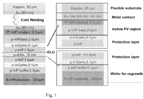
are eliminated as shown in Figure 1.
[032] Accordingly, the surface of the processed wafer can be made smoother
than the starting wafer, and its surface chemistry also remains unchanged,
hence
removing the need for wafer re-polishing prior to reuse for growth of
additional, and also
ultimately removable, epitaxial layers. Thus, the parent wafer can be reused
indefinitely,
as none of the original parent wafer is consumed or altered during the
process. Indeed,
only the epitaxial active layers that comprise the thin-film, single-crystal,
high-efficiency
solar cell active region are removed from the entire wafer surface, and
subsequently
cold-welded (without adhesives that add cost, weight and potential for
failure) to a
second, thin-film "host" substrate.
[033] Since the substrate is the most costly material used in the process,
the
multiple-reuse strategy removes the wafer as a material's cost, and transforms
its
13
CA 02840968 2014-01-03
WO 2013/006803
PCT/US2012/045778
acquisition into a capital expense, fundamentally changing the cost structure
of single
crystal III-V-based solar cells. If the very thin, active epitaxial layers of
the solar cell are
also bonded to a metal or metalized plastic foil without using adhesives, the
cost, weight
and form factor of the resulting module is also favorably impacted.
[034] In an effort to address at least some of the foregoing described needs,
there is disclosed an ultrahigh-efficiency single- and multi-junction thin-
film solar cell.
The present disclosure is also directed to a substrate-damage-free epitaxial
lift-off
("ELO") process that employs adhesive-free, reliable and lightweight cold-weld
bonding
to a substrate, such as bonding to plastic or metal foils shaped into compound
parabolic
metal foil concentrators. The Inventors have discovered that combining low-
cost solar
cell production and ultrahigh-efficiency of solar intensity-concentrated thin-
film solar
cells on foil substrates shaped into an integrated collector, can result not
only in lower
cost of the module itself, but also in significant cost reductions in the
infrastructure by
replacing heavy modules with ultra-lightweight cells on foils (including low-
cost
integrated concentrators), with power densities exceeding 6 W/gm.
[035] In one embodiment, the present disclosure is directed to a thin-film
solar
cell comprising a first substrate; a metal contact bonded to said first
substrate; an active
photovoltaic region bonded to said metal contact; one or more first protection
layers; an
AIAs layer; one or more second protection layers; and a second substrate,
wherein said
second substrate.
[036] In another embodiment, the present disclosure is directed to a thin-film
solar cell comprising a first substrate; a metal contact bonded to said first
substrate; an
active photovoltaic region bonded to said metal contact; one or more first
protection
14
CA 02840968 2014-01-03
WO 2013/006803
PCT/US2012/045778
layers, wherein at least one of said first protection layers comprise at least
one
compound chosen from InGaP, GaAs, InGaAs, InP, and InAlP; an AlAs layer; one
or
more second protection layers, wherein at least one of said second protection
layers
comprise at least one compound chosen from InGaP, GaAs, InGaAs, InP, and
InAlP;
and a second substrate, wherein said second substrate comprises at least one
compound chosen from GaAs and InP.
[037] In a further embodiment, the present disclosure is directed to a method
for performing an epitaxial lift-off process, comprising growing one or more
first
protection layers on a first substrate; growing an AlAs layer; growing one or
more
second protection layers; depositing at least one active photovoltaic cell
layers on top of
the second protection layer; coating the top active photovoltaic cell layer
with a metal;
coating a second substrate with a metal; pressing together the two metal
surfaces to
form a cold-weld bond; and removing the AlAs layer with a selective chemical
etchant.
[038] In another embodiment, the present disclosure is directed to a method
for performing an epitaxial lift-off process, comprising growing one or more
first
protection layers on a first substrate, wherein at least one of said
protection layers
comprise a compound chosen from InGaP, GaAs, InGaAs, InP, and InAlP; growing
an
AlAs layer; growing one or more second protection layers, wherein at least one
of said
protection layers comprise a compound chosen from InGaP, GaAs, InGaAs, InP,
and
InAlP; depositing at least one active photovoltaic cell layers on top of the
second
protection layer; coating the top active photovoltaic cell layer with a metal;
coating a
second substrate with a metal; pressing together the two metal surfaces to
form a cold-
weld bond; and removing the AlAs layer with a selective chemical etchant.
CA 02840968 2014-01-03
WO 2013/006803
PCT/US2012/045778
[039] Aside from the subject matter discussed above, the present disclosure
includes a number of other exemplary features such as those explained
hereinafter. It
is to be understood that both the foregoing description and the following
description are
exemplary only.
[040] The accompanying figures are incorporated in, and constitute a part of,
this specification.
[041] Fig. 1. Is a schematic showing the ELO process according to the
present disclosure for InP based solar cells.
[042] Fig. 2. Is a photograph of a two inch InP epitaxial layer lifted off
and
bonded to a Au-coated Kaption sheet. ITO contacts form the Schotty solar
cells.
[043] Fig. 3. Is an atomic force microscope image of the original epi-ready
InP
substrate and recovered surfaces after the first and second ELO processes,
with and
without the use of protection layers.
[044] Fig. 4. Is test data and a representative GaAs PV cell layer
structure
showing cell parameters.
[045] Fig. 5. Is test data showing fourth quadrant current voltage and
external
quantum efficiency (inset) of a 23.9% efficient first-growth cell and a 22.8%
efficient cell
grown on a reused wafer.
[046] Fig. 6. Is a schematic showing the ELO process as applied to an InP
material according to the present disclosure.
[047] Fig. 7. Is a schematic of a trilayer protection scheme with AIAs
layer and
AIAs lift-off layer.
16
CA 02840968 2014-01-03
WO 2013/006803
PCT/US2012/045778
[048] Fig. 8. Is a schematic of a proposed multi-junction cell structure
according to the present disclosure.
[049] Fig. 9. Is a schematic of (a) conventional N/P tunnel junctions, and
(b)
N/ErP/P junction showing the reduced tunneling barriers.
[050] Fig. 10. Is a schematic of an integrated reflector with cold-welded
bonded ELO multi-junction cell.
[051] One embodiment of the ELO process is shown schematically in Fig. 1. It
begins with the epitaxial growth of the chemically distinct, thin "protection
layers"
consisting of InGaAs and InP, a sacrificial layer of AIAs, a second set of
protection
layers of InP and InGaAs, and finally the active photovoltaic cell layers.
Next, the top
epitaxial layer is coated with Au, as is a very thin plastic (e.g. KaptonTM, a
polyimide film
marked by DuPont) host substrate. By pressing the two clean Au surfaces
together at
only a few kPa pressure, they form an electronically continuous and permanent,
adhesive-free cold-weld bond whose properties are indistinguishable from a
single, bulk
Au film.
[052] Once bonded to the plastic handle, the wafer is ready for ELO. The
cold-
weld bond is used not only for the ELO process (the epi-layer is attached
permanently
to the foil substrate prior to the liftoff, peeling away the parent substrate
for eventual
reuse) but also as the adhesive to the new host substrate on which the solar
cells are
eventually fabricated.
[053] Replacement of adhesives conventionally used in lift-off by the cold-
weld has several benefits: (i) attachment to the foil substrate is simple and
is an integral
part of the fabrication sequence, (ii) it is lightweight as it completely
eliminates an
17
CA 02840968 2014-01-03
WO 2013/006803
PCT/US2012/045778
adhesive layer, (iii) it is thermally and electrical "transparent" since the
cold-weld
interface is indistinguishable from the bulk of the film, and (iv) it is
robust and resistant
to failure. A selective chemical etchant, such as HF: H20, 1:10, is used to
remove the 4
nm to 10 nm-thick AIAs sacrificial ELO layer, parting the entire wafer from
the
photovoltaic epitaxial layers, leaving the protection layers exposed. The
purpose of the
protection layer nearest the AlAs ELO layer (InP in this case) is to provide
an etch
selectivity >108:1 and is removed from both the substrate and the parted
epitaxial layers
with a second wet etch (HCI:H3PO4, 3:1) that stops at the InGaAs protection
layer
surface. The requirements of the second protection layer are that it can be
removed
with a wet etchant that stops abruptly at the InP substrate. The InGaAs layer
is removed
from the wafer using H2SO4:H202:H20 (1:1:10), followed by C6H807:H202 (20:1),
both of
which have high selectivity to the InP substrate, InP buffer, and epitaxial
layers, and
assist in the removal of any debris or asperities remaining after the previous
etch. Solar
cells are fabricated on the epitaxial layers that are attached to the KaptonTM
handle by
sputtering indium tin oxide (ITO) Schottky contacts. The resulting flexible
InP-ITO
Schottky solar cells with efficiencies of -15% under 1 sun AM1.5G illumination
are
shown in Fig. 2. These bonded epitaxial sheets have been repeatedly cycled to
>200 C
without delamination.
[054] Previous to subsequent growth, the substrate is solvent cleaned,
an
intentional oxide is grown via exposure to UV/Ozone, and then returned to the
growth
chamber. The process has been employed multiple times with a single substrate
to
demonstrate degradation-free reuse of InP wafers, and as shown in Fig. 3, the
18
CA 02840968 2014-01-03
WO 2013/006803
PCT/US2012/045778
smoothness of the surface can be improved over that of the commercial epi-
ready
wafers that are initially used, in principle allowing for indefinite reuse.
[055] The Inventors have recently extended this damage-free regrowth
process to GaAs-based single p-n junction photovoltaic cells fabricated on a
parent
wafer, resulting in efficiencies of 23.9%. Fig. 4 is a schematic
representation of such a
cell. The lift-off process is similar to that used for the InP cells, although
the two-
protection-layer scheme used for InP is replaced by a three-layer
(InGaP/GaAs/InGaP),
fully lattice-matched (to the AIAs sacrificial layer) system. This allows for
improved etch-
selectivity between layers while eliminating debris or surface roughening
incurred in the
ELO process. The AIAs layer is removed in HF, followed by removal of the InGaP
and
GaAs protection layers with HCI:H3PO4 (1:1) and H3PO4:H202:H20 (3:1:25),
respectively.
[056] Following this process, a second cell is grown on the parent wafer,
reaching an efficiency of 22.8%. The slight (1%) reduction in power conversion
efficiency between the first and second growths is due to the choice of the
dry mesa-
isolation etch recipe, resulting in a slight reduction in fill factor (see
Fig. 4). Furthermore,
the anti-reflection coating thickness was not optimal, reducing the external
quantum
efficiency and short circuit current as shown in Fig. 5. However, even higher
efficiencies, for example greater than 25%, are expected when the coating
thickness is
optimized.
[057] In one embodiment, a protection layer scheme based on the fully
lattice-
matched InGaP/GaAs/InGaP trilayer can be used. This tri-layer affords etch
chemistries
with sufficient rate selectivity between layers required to reproducibly
remove the
19
CA 02840968 2014-01-03
WO 2013/006803
PCT/US2012/045778
protection layers and to expose a pristine (physically and chemically
undamaged)
surface. In one embodiment, regrown thin-film cells are bonded via cold-
welding to Au-
coated plastic (KaptonTM) substrates. It has been shown that a PCE=23.9% for a
first
growth wafer, and PCE=22.8% for a reused wafer can be achieved, which exceeds
the
Next Generation Photovoltaics II metric of 20% (see Fig. 5). A depiction of
the actual
ELO process apparatus and method are shown in Fig. 6.
[058] Following each reuse, both the parent wafer and the lifted off
epitaxial
layers can be thoroughly studied for damage or subtle degradation. These
methods
include x-ray photoelectron spectroscopy (XPS) to determine chemical changes
to the
growth and regrowth surfaces, atomic force microscopy, scanning electron
microscopy,
and surface profilometry to determine surface morphological changes, cross-
sectional
transmission electron microscopy to examine defects that are incurred within
the bulk of
the epitaxy, and compositional depth profiling using secondary ion mass
spectroscopy
(SIMS).
[059] Completed cells, including anti-reflection coating, can also be
electrically
tested using standard illumination conditions (1 sun, AM1.5G spectrum).
Parameters to
be measured include PCE, fill factor (FF), open circuit voltage (Voc), short
circuit current
(Jsc), series and parallel resistance.
[060] It has been found that extended exposure (>2 days) of Ga-containing
compounds (i.e. GaAs, and to a lesser degree InGaP) to HF results in surface
contamination that is difficult to remove. This reaction, however, is absent
for InP
surfaces exposed to HF for over 7 days. In one embodiment a thin layer of
strained InP
CA 02840968 2014-01-03
WO 2013/006803
PCT/US2012/045778
placed immediately below the AlAs sacrificial layer will improve the fidelity
of the
surface, as shown in Fig. 7.
[061] The thickness of the InP is limited to prevent strain relaxation,
which can
degrade the subsequently grown PV layer quality. The critical thickness of InP
on GaAs
is between 5 and 6 monolayers, corresponding to -1.7 nm. In this case the
protection
layer scheme would comprise InGaP/GaAs/InP or InGaP/GaAs/InGaP/InP, where the
additional InGaP layer in the latter structure provides improved protection
above the
GaAs.
[062] In another embodiment, the etch selectivity and preservation of the
as-
purchased wafer quality is carried out by using additional materials
combinations, for
example by replacing the InGaP layer adjacent to the InAlP. An
InAlP/InGaP/GaAs/InAlP structure may be advantageous since InAlP can be etched
with HCI:H20 (1:5), which stops abruptly at GaAs (>400:1 etch ratio), whereas
HCI:H3PO4(1:1) used to etch InGaP slowly attacks the GaAs which results in
roughening. By placing the InAlP adjacent to the AlAs layer, the InAlP is
attacked by the
HF and reduces the buildup of arsenic oxide which can slow the liftoff
process. Also,
InGaP may be used as an etch stop for the GaAs etch (H3PO4:H202:H20, 3:1:25)
to
ensure that the lower InAlP layer is only removed in the final etch step.
[063] Additional cost reduction may be possible by bonding to metal-foil
substrates such as Au-coated Cu foils, use of less expensive metals for cold-
welding
(e.g. Ag instead of Au), reduced consumption of HF, reduced protection layer
thicknesses, and accelerating the lift-off process. The extended exposure to
HF used to
dissolve the AlAs sacrificial layer limits the choice of metal host substrates
that can be
21
CA 02840968 2014-01-03
WO 2013/006803
PCT/US2012/045778
employed. In one embodiment, Cu foils, which can be used for cold-welding, are
used
to increase resistance upon exposure to HF, as their use may be simpler than
coating
the foil with a noble metal such as Au. An additional benefit to using Cu foil
is its high
thermal conductivity (-4W cm-1*C-1) that can be exploited to extract heat from
the
concentrated cells.
[064] There is also disclosed very high-efficiency multi-junction
(GaAs/InGaP)
solar cells following the two cell example structure shown in Fig. 8.
[065] The design is inverted relative to a conventional multi-junction cell
growth sequence to accommodate the "upside down" bonding geometry used in the
adhesive-free cold-weld process; the structure includes a 25% GaAs cell
architecture.
In this case, the GaAs cell thickness is reduced to 2 pm (50% of the
conventional
substrate-based cell) since the reflective, full-coverage ohmic contact allows
for two
passes of the incident light through the device active region. The primary
focus will be
on optimizing the tandem PV structure for maximum efficiency, including InGaP
cell
design (layer thickness, window layer, layer composition, etc.), improving the
wide-gap
tunnel junctions (TJ) between elements in the stack, and perfecting the
multiple lift-off
process over large areas for this multi-junction cell.
[066] Solar cells will be grown with n-type material on top of p-type
layers,
whereas the tunnel junctions must be grown with the opposite polarity. The
cells may
employ carbon-doping in all or several of the p-type layers, since carbon does
not
readily migrate to the growth surface as does the conventional p-dopant, Be.
As the
tandem cells are generally limited by the current in the GaAs cell, the InGaP
cell
22
CA 02840968 2014-01-03
WO 2013/006803
PCT/US2012/045778
thickness needs to be adjusted to current-match the InGaP and GaAs cells; the
thickness of the InGaP layer is expected to range from 0.55 to 0.80 pm.
[067] Efficient tunnel junctions (TJ) are essential for high performance
tandem
cells. They need to be nearly loss-less in both voltage and absorption. It is
advantageous to use an InGaP TJ in MJ cells to avoid GaAs TJ absorption that
may be
as high as 3%. A conventional TJ is an abrupt P+/N+ junction where the
electron can
tunnel directly from the conduction band on the n-type side to the valence
band on the
p-type side (Fig.9(a)). Little work has been performed on MBE grown wide gap
TJs,
although doping levels that are sufficiently high to transport currents
generated at 1 sun
illumination have been reported using MBE.
[068] One embodiment is directed to InGaP tunnel junctions that have a
voltage drop of several tens of mV at 1 sun. Research suggests that Be and Si
are
suitable dopants (attaining densities of 3.7x10¹⁹ and 1.8x1019 cm-3,
respectively).
However, if a reduced tunneling resistance is required, the use of engineered
defects at
the P+/N+ interface, can be done, such as by adding ErAs to a GaAs tunnel
junction. In
this case, ErP or LuP may be used as shown in Fig. 9b. The ErP or LuP form
epitaxial
islands on the semiconductor surface that are ¨ 4 monolayers thick, are
metallic, and
split the tunneling process into two steps with significantly higher tunneling
probabilities.
By employing ErP in the TJ, several orders of magnitude increase in the
tunneling
current may result, and lead to voltage drops in the sub-mV range for the
currents
anticipated in the fabricated PV cells.
[069] As in the case of the single junction cells, the multi-junction cell
can be
microscopically and chemically examined after each iteration of the growth-ELO-
reuse
23
CA 02840968 2014-01-03
WO 2013/006803
PCT/US2012/045778
cycle. Completed cells, including anti-reflection coating, can be electrically
tested using
standard illumination conditions (AM1.5G spectrum), but over a range of
intensities up
to 10 suns. Parameters to be measured include PCE, fill factor, open circuit
voltage,
short circuit current, series and parallel resistance, as in the case of the
single junction
cells.
[070] Thin-film multi-junction cells bonded onto reflective and flexible
substrates provide a unique opportunity to integrate the solar collector with
the thin-film
cell without introducing significant additional costs. Fig. 10 shows that a
strip consisting
of the ELO multi-junction cell is bonded to the center of a larger, flexible,
reflective film.
The film is then molded (by placement in a thermally conductive or actively
cooled
preform) into the shape of a compound parabolic collector (e.g. a CPC, or
Winston
collector). This geometry concentrates parallel solar rays onto the cell strip
at its focus,
as well as collects diffuse light within the acceptance cone.
[071] The small levels of concentration (4-10X) generally used in the
cylindrical Winston-type collectors allow the concentrators to be highly
efficient, and to
direct a significant amount to diffuse light into the cell. The efficiency of
collection is
given by CEff=Tcpcy, where Tcpc is the effective transmittance of the CPC,
including
losses of multiple bounces that are -2% for common reflector materials. The
correction
for diffuse light is y=1-(1-1/C)Gdiff/Gdir, where C is the intended
concentration, and
Gdiff/Gdir is the fraction of diffuse to total incident light. Typically,
Gdiff/Gdir-0.11 for a
low-cloudiness day. Then for C=4, y=90% at AM1.5G, which is comparable to the
power
available at AM1.5D.
24
CA 02840968 2014-01-03
WO 2013/006803
PCT/US2012/045778
[072] For a 4X CPC, and assuming a solar cell strip width of 1 cm, the
aperture is then 4 cm wide x 10 cm deep, providing a practical form factor
compatible
with panels used in single family dwellings. At higher concentrations, the
size of the
concentrator increases considerably. For example, a 10X concentration used
with the
same 1 cm wide cell strip requires an aperture of 10cm with a depth of ¨ 55cm.
This can
be reduced to ¨40cm with negligible effect on concentration efficiency. [25]
The amount
of reflective material needed is 4-5 times larger for 4X concentration, and 8-
11 times for
10X concentration.
[073] Additional benefits to the small concentrations used include the allowed
use of single-axis tracking (daily or seasonally, depending on orientation of
the
collector), and simplified passive cooling than are needed for higher
concentrations.
Indeed, the very thin substrates used greatly simplify heat transfer:
calculations indicate
that at 10X concentration and a 25mm thick KaptonTM substrate placed against a
passively cooled Cu heat sink results in a temperature rise of only 5-20 C,
obviating the
need for more aggressive cooling methods.
[074] Note that the ELO cell technology can also be applied to systems with
large concentration factors; however, here the present disclosure focused only
on
smaller concentrations that lead to simple and economical designs that are
applicable to
residential systems. The cost reductions in this integrated solar collector +
ELO multi-
junction concentrator cell assembly is expected to radically reduce the cost
of
concentrated systems, as well as their footprint (owing to the high PCE).
[075] Unless otherwise indicated, all numbers expressing quantities of
ingredients, reaction conditions, and so forth used in the specification and
claims are to
CA 02840968 2014-01-03
WO 2013/006803
PCT/US2012/045778
be understood as being modified in all instances by the term "about."
Accordingly,
unless indicated to the contrary, the numerical parameters set forth in the
following
specification and attached claims are approximations that may vary depending
upon the
desired properties sought to be obtained by the present invention.
[076]
Other embodiments of the invention will be apparent to those skilled in
the art from consideration of the specification and practice of the invention
disclosed
herein. It is intended that the specification and examples be considered as
exemplary
only, with the true scope of the invention being indicated by the following
claims.
26