Note: Descriptions are shown in the official language in which they were submitted.
ELECTRODES, ELECTRODE SYSTEMS, AND METHODS OF MANUFACTURE
Background
[0002] Conventional electrodes for medical use suffer from a number of
drawbacks. First,
some electrodes are hand-manufactured by manually separating the strands of
one end of a
multi-strand wire and fanning each of these strands to a conductive polymer
impregnated
with carbon to form an electrode and a pigtail. A separate connector is then
attached to the
other end of the multi-strand wire, often by hand-soldering. Using a multi-
strand wire as an
electrode pigtail results in a number of discrete contact points between the
wire and the
conductive polymer, each of which may form a "hotspot" that disrupts even
current
distribution over the surface of the electrode and may burn the patient during
electrostimulation therapy. Non-uniformities in the connections between the
strands of the
wire and the conductive polymer may also increase the risk of hotspots. Such
electrodes
cannot be cut or readily fabricated in the range of shapes that clinicians and
patients would
like in order to provide targeted and customized therapy. Some electrodes
include snap
connectors instead of pigtails, which also suffer from the risk of hotspots
and can be difficult
to connect and disconnect to an electrostimulation lead.
Summary
100031 Described herein are electrodes, electrode connectors, stimulation
systems, and
methods of assembling the same. In one aspect, an electrode is provided. In
certain
implementations, the electrode includes a conductive layer having a first area
designed for
application of therapeutic electrical stimulation to a patient's tissue and a
second area
including a tail configured as a unitary extension of the first area. In some
implementations,
the conductive layer is made of aluminum. A connector is disposed on a distal
end of the tail
and a nonconductive top layer is disposed along a top portion of the
conductive layer. In
some implementations, a tip of the distal end of the tail is flared. The
flared tip may form a
tube with an inner passage configured to receive a male pin. In some
implementations, the
connector includes a connector housing with an undulating receptacle. The
distal end of the
-
CA 2841950 2018-05-29
CA 02841950 2014-01-14
WO 2013/012465 PCT/US2012/033575
tail may connect to a conducting connection portion of the undulating
receptacle. In some
implementations, the distal end of the tail is crimped or glued to a connector
configured to
couple with a lead from an electrical stimulation generator.
[0004] In some implementations, a second conductive layer is disposed on the
distal end of
the unitary tail. The second conductive layer and the distal end of the
unitary tail may be
formed into a tube with an inner passage that is configured to receive a male
pin from an
electrical stimulation lead. The second conductive layer may be a carbon
strip, or a
conductive polyvinylchloride or polyurethane impregnated with carbon, for
example.
[0005] In some implementations, the electrode includes a gel layer disposed
beneath the
conductive layer. In some implementations, the electrode includes a
nonconductive bottom
layer disposed along a bottom portion of the tail of the conductive layer. The
nonconductive
bottom layer may include an extension portion disposed partially beneath the
conductive
layer. The extension portion of the bottom layer may also be disposed
partially beneath a gel
layer. In some implementations, the conductive layer has a perimeter side
surface and a gel
coating disposed at least partially about the perimeter side surface. The gel
coating may
extend around the entire perimeter of the side surface.
[0006] In certain implementations, the electrode includes a nonconductive top
layer, a
conductive layer disposed beneath the nonconductive top layer, a gel layer
disposed beneath
the conductive layer; and a snap connector. The snap connector includes a
first conductive
housing disposed above the nonconductive top layer and a second housing
disposed beneath
the conductive layer, the second housing being at least partially
nonconductive and
configured to join the first conductive housing to span the conductive layer
and the
nonconductive top layer. In some implementations, the second housing includes
a second
conductive housing disposed between a nonconductive element and the first
conductive
housing, with the second conductive housing disposed beneath the conductive
layer. The
nonconductive element may be a polymer. In some implementations, the
conductive layer
has a perimeter side surface and a gel coating disposed at least partially
about the perimeter
side surface. The gel coating may extend around the entire perimeter of the
side surface.
[0007] In certain implementations, the electrode includes a conductive layer,
a conductive
magnetic layer disposed along a top portion of the conductive layer, a
nonconductive top
layer disposed along a top portion of the conductive magnetic layer, and a
socket disposed
along a top portion of the nonconductive top layer and configured to receive a
magnetic lead
connector. In some implementations, the conductive layer is aluminum. In some
implementations, the conductive magnetic layer includes a ferritic material,
such as stainless
-2-
CA 02841950 2014-01-14
WO 2013/012465 PCMJS2012/033575
steel. In some implementations, a diameter of the conductive magnetic layer is
smaller than a
diameter of the conductive layer. In some implementations, the socket has a
base portion
with a base diameter and a top portion with a top diameter, the base diameter
larger than the
top diameter. The base portion may be disposed below the nonconductive top
layer and the
.. top portion may be disposed above the nonconductive top layer.
[0008] In certain implementations, the electrode includes a nonconductive top
layer, a
conductive layer disposed beneath the nonconductive top layer, a gel layer
disposed beneath
the conductive layer, and a receptacle structured as a depression in the
conductive layer
configured to receive a male connector of a lead from an electrostimulation
system. A
nonconductive element is disposed beneath the receptacle. In some
implementations, the
receptacle is configured to receive a male snap connector. In some
implementations, the
nonconductive element is disposed between a bottom surface of the receptacle
and a bottom
surface of the gel layer.
[0009] In another aspect, an electrode system is provided. In certain
implementations, the
electrode system includes a plurality of conductive zones, each conductive
zone including an
electrode having a conductive layer with a unitary tail. The electrode system
also includes a
plurality of connectors, each connector disposed on a distal end of each of
the unitary tails,
and a nonconductive top layer disposed above the conductive zones The
plurality of
conducting zones may be separated laterally by an insulating foam layer. In
some
implementations, the plurality of conducting zones are disposed symmetrically
about a hole
in the nonconductive top layer. The plurality of conductive zones may be
disposed
concentrically about the hole in the nonconductive top layer. In some
implementations, a
first of the plurality of conductive zones is disposed between a second of the
plurality of
conductive zones and the nonconductive top layer. A nonconductive layer may
also be
disposed between the a portion of the first of the plurality of conductive
zones and the second
of the plurality of conductive zones.
[0010] In certain implementations, the electrode system includes an electrode
having a
socket configured to receive a magnetic lead connector and a lead including a
magnetic lead
connector, the magnetic lead connector including a magnet configured to seat
within the
socket. The magnetic lead connector may include an outer wall configured to
capture at least
a portion of the socket between the outer wall and the magnet.
[0011] In some implementations of the electrode and electrode systems
described herein, a
nonconductive layer is formed in a non-radially symmetric shape. The non-
radially
-3-
CA 02841950 2014-01-14
WO 2013/012465 PCMJS2012/033575
symmetric shape may be rectangular. In some implementations of the electrode
and electrode
systems described herein, a nonconductive layer is formed in an asymmetric
shape.
[0012] In another aspect, a stimulation system is provided. In certain
implementations, the
stimulation system includes a nonconductive top layer and an electronics
layer, disposed
beneath the nonconductive top layer. The electronics layer includes pulse
generation
circuitry in electrical communication with a first conductive contact point in
the electronics
layer. The stimulation system also includes a conductive layer, disposed
beneath the
electronics layer, having a second conductive contact point in electrical
contact and
alignment with the first conductive contact point via a puncture connection
between the
electronics layer and the conductive layer. In some implementations, the
stimulation system
includes a second conductive layer, disposed beneath the electronics layer.
The second
conductive layer has a third conductive contact point in electrical contact
and alignment with
a fourth conductive contact point in the electronics layer via a puncture
connection between
the electronics layer and the second conductive layer. The stimulation system
may include
any of the electrode or electrode systems described herein.
[0013] In another aspect, an iontophoresis delivery system is provided. In
certain
implementations, the iontophoresis delivery system includes a conductive layer
and a drug
delivery layer. The drug delivery layer includes a therapeutic compound, and
is arranged to
deliver the therapeutic compound into a patient's tissue when a DC current is
driven into the
patient's tissue from the conductive layer. The iontophoresis delivery system
also includes an
electronics layer comprising pulse generation circuitry. The pulse generation
circuitry is
configured to deliver the DC current to the conductive layer for a
predetermined period of
time to drive the therapeutic compound into the patient's tissue, and after
delivering the DC
current for the predetermined period of time, deliver an AC TENS current to
the conductive
layer. In some implementations, the iontophoresis delivery system also
includes a battery
and the pulse generation circuitry is configured to use the battery to power
the delivery of the
DC current and the delivery of the AC TENS current. In some implementations,
the
iontophoresis delivery system includes a chemical switch configured to
indicate that the
predetermined period of time has elapsed when a predetermined amount of
therapeutic
compound has been driven into the patient's tissue.
[0014] In another aspect, a method of assembling an electrode is provided. In
certain
implementations, the method includes providing a conductive layer having a
first area
designed for application of therapeutic electrical stimulation to a patient's
tissue and a second
area including a tail configured as a unitary extension of the first area,
disposing a
-4-
CA 02841950 2014-01-14
WO 2013/012465 PCMJS2012/033575
nonconductive top layer along a top portion of the conductive layer, and
forming a connector
at the distal end of the tail. Forming a connector at the distal end of the
tail may include
inserting the distal end of the tail into a receptacle and crimping the
receptacle to secure the
distal end of the tail within the receptacle. The distal end of the tail may
include a flared
portion with first and second sides, in which case forming a connector may
include securing
the first and second sides in proximity to one another to form a tube from the
flared portion.
The securing may include arranging the first and second sides in proximity
with one another,
disposing a length of heat-shrink tubing around the flared portion when the
first and second
sides are arranged in proximity, and heating the heat-shrink tubing to reduce
the diameter of
the heat-shrink tubing around the flared portion, thereby capturing the flared
portion in a
tubular configuration.
[0015] In another aspect, a method of assembling an electrode is provided. In
certain
implementations, the method includes providing a conductive layer, forming a
depression in a
top surface of the conductive layer, the depression configured as a receptacle
for receiving a
male connector of a lead from an electrostimulation system, and disposing a
gel layer on a
bottom surface of the conductive layer. In some implementations, the method
also includes
disposing a nonconductive element beneath the depression, between the bottom
surface of the
conductive layer and a bottom surface of the gel layer.
[0016] In another aspect, a method of assembling an electrode system is
provided. In
certain implementations, the method includes providing a first ring-shaped
conductive layer,
disposing a ring-shaped conductive layer within an interior of the first ring-
shaped conductive
layer, disposing a second conductive layer within an interior of the ring-
shaped conductive
layer, and disposing a nonconductive top layer along a top portion of the
first and second
ring-shaped conductive layers. The second conductive layer may be ring-shaped.
[0017] In another aspect, a method of assembling a stimulation system is
provided. In
certain implementations, the method includes providing an electronics layer
including pulse
generation circuitry in electrical communication with a first conductive
contact point in the
electronics layer, disposing a conductive layer beneath the electronics layer,
and puncturing
the electronics layer and the conductive layer at the first conductive contact
point to form an
electrical connection between the conductive contact point of the electronics
layer and the
conductive layer. In some implementations, the method further includes
disposing a gel layer
beneath the conductive layer and disposing a nonconductive top layer above the
electronics
layer. In some implementations, the electronics layer includes one or more
switches
configured to control the pulse generation circuitry, and the method further
includes
-5-
disposing one or more buttons in alignment with the one or more switches such
that pressing the
one or more buttons activates the corresponding one or more switches. In some
implementations,
the one or more switches includes a power-on switch and pressing the button
associated with the
power-on switch initiates delivery of electrical pulses from the pulse
generation circuitry to the
conductive layer.
[0017a] In one embodiment, there is provided an electrode including a first
conductive layer
having a first area designed for application of therapeutic electrical
stimulation to a patient's
tissue and a second area including a tail configured as a unitary extension of
the first area. The
electrode further includes a gel layer disposed beneath the first conductive
layer and a connector
disposed on a distal end of the unitary tail. A portion of the distal end of
the unitary tail is flared.
The flared portion comprises first and second sides secured in proximity to
one another to form a
tube by a heat-shrink tubing around the flared portion. The heat-shrink tubing
is adapted to
provide mechanical support for the tube and the unitary tail and insulation
between the tube and a
user of the electrode. An inner passage of the tube is configured to receive a
male pin from an
electrical stimulation lead. The electrode further includes a second
conductive layer disposed on
the flared portion of the distal end of the unitary tail. The second
conductive layer is adapted to
strengthen the connector against wear and tear of connection and
disconnection, The electrode
further includes a nonconductive bottom layer disposed along a bottom portion
of the unitary tail
of the first conductive layer. The nonconductive bottom layer includes an
extension portion
disposed partially beneath the first conductive layer. The extension portion
of the bottom layer is
also disposed partially beneath the gel layer. The electrode further includes
a nonconductive top
layer disposed along a top portion of the first conductive layer.
[0017b] The first conductive layer may be made of aluminum.
[0017c] The connector may include a connector housing with an undulating
receptacle.
[0017d] The distal end of the unitary tail may connect to a conducting
connection portion of the
undulating receptacle.
[0017e] The distal end of the tail may be crimped or glued to a connector
configured to couple
with a lead from an electrical stimulation generator.
[00171] The second conductive layer may be a carbon strip.
[0017g] The second conductive layer may be conductive polyvinylchloride or
polyurethane
impregnated with carbon.
-5a-
CA 2841950 2020-03-19
[0017h] The first conductive layer may have a perimeter side surface and a gel
coating disposed
at least partially about the perimeter side surface.
[0017i] The gel coating may extend around the entire perimeter of the side
surface.
[0017j] The nonconductive layer may be formed in a non-radially symmetric
shape.
[0017k] The non-radially symmetric shape may be rectangular.
[00171] The nonconductive layer may be formed in an asymmetric shape.
[0017m] In another embodiment, there is provided a method of assembling an
electrode. The
method involves providing a first conductive layer having a first area
designed for application of
therapeutic electrical stimulation to a patient's tissue and a second area
including a tail configured
as a unitary extension of the first area. A distal end of the unitary tail
comprises a flared portion
including first and second sides. The method further involves providing a
second conductive
layer disposed on the distal end of the unitary tail, providing a gel layer
disposed beneath the first
conductive layer, and providing a nonconductive bottom layer disposed along a
bottom portion of
the unitary tail of the first conductive layer. The nonconductive bottom layer
includes an
.. extension portion disposed partially beneath the first conductive layer.
The extension portion of
the bottom layer is also disposed partially beneath the gel layer. The method
further involves
disposing a nonconductive top layer along a top portion of the first
conductive layer and forming
a connector at the distal end of the unitary tail by securing the first and
second sides in proximity
to one another to form a tube from the second conductive layer and the flared
portion. An inner
.. passage of the tube is configured to receive a male pin from an electrical
stimulation lead.
Securing the first and second sides in proximity to one another involves
arranging the first and
second sides in proximity with one another, disposing a length of heat-shrink:
tubing around the
flared portion when the first and second sides are arranged in proximity, and
heating the heat-
shrink tubing to reduce the diameter of the heat-shrink tubing around the
flared portion, thereby
capturing the flared portion in a tubular configuration.
[0017n] Forming a connector at the distal end of the tail may involve
inserting the distal end of
the unitary tail into a receptacle and crimping the receptacle to secure the
distal end of the unitary
tail within the receptacle.
-5b-
CA 2841950 2020-03-19
[0017p] The distal end of the tail may include a flared portion including
first and second
sides. Forming a connector at the distal end of the tail may involve securing
the first and
second sides in proximity to one another to form a tube from the flared
portion.
[0017q] Securing the first and second sides in proximity to one another may
involve
arranging the first and second sides in proximity with one another, disposing
a length of heat-
shrink tubing around the flared portion when the first and second sides are
arranged in
proximity, and heating the heat-shrink tubing to reduce the diameter of the
heat-shrink tubing
around the flared portion, thereby capturing the flared portion in a tubular
configuration.
-5c-
CA 2841950 2019-03-18
[0018] In another aspect, a method of configuring a single device for the
delivery of
iontophoretic and TENS treatments is provided. In certain implementations, the
method
includes providing an electrical stimulation system having a conductive layer,
a drug delivery
layer with a therapeutic compound, and pulse generation circuitry. The method
may further
include configuring the pulse generation circuitry to, upon activation when
positioned on a
patient's tissue, deliver a DC current to the conductive layer for a
predetermined period of
time to drive the therapeutic compound from the drug delivery layer into the
patient's tissue
and after delivering the DC current for the predetermined period of time,
deliver an AC
TENS current to the conductive layer. In some implementations, the pulse
generation
circuitry includes a battery and the method further includes configuring the
pulse generation
circuitry to use the battery to power the delivery of the DC current and the
delivery of the AC
TENS current. In some implementations, the method further includes configuring
the pulse
generation circuitry to deliver the AC TENS current until the battery is
depleted.
[0019] Variations and modifications will occur to those of skill in the
art after reviewing
this disclosure, where disclosed features may be implemented in any
combination and
subeombinations (including multiple dependent combinations and
subcombinations), with
one or more other features described herein. The various features described or
illustrated
above, including any components thereof, may be combined or integrated in
other systems;
moreover, certain features may be omitted or not implemented.
[0020] Examples of changes, substitutions and alterations are ascertainable
by one skilled
in the art and to be made without departing from the scope of the information
disclosed
herein.
Brief Description of the Drawings
[0021] The foregoing and other objects and advantages will be appreciated
more fully
from the following description, with reference to the accompanying drawings
wherein:
[0022] FIG. 1A is an exploded view of a unibody electrode;
100231 FIG. 1B is a plan view of certain components of the unibody
electrode of FIG. 1A;
-6-
CA 2841950 2018-05-29
CA 02841950 2014-01-14
WO 2013/012465 PCMJS2012/033575
[0024] FIGS. 2A and 2B are perspective views of a connector;
[0025] FIG. 3 is an exploded view of another unibody electrode;
[0026] FIGS. 4A-4C are perspective views of another connector;
[0027] FIGS. 5 and 6 are exploded views of snap electrodes;
[0028] FIGS. 7 and 8 are exploded views of magnetic connector electrodes;
[0029] FIG. 9 is a perspective view of a magnetic lead connector;
[0030] FIG. 10A is an exploded view of an inverted snap electrode, and FIG.
10B is a
cross-sectional view of the inverted snap electrode of FIG. 10A;
[0031] FIG. 11 is a perspective view of a connector for an inverted snap
electrode;
[0032] FIG. 12 is an exploded view of an electrode system;
[0033] FIG. 13 is an exploded view of another electrode system;
[0034] FIG. 14 is an exploded view of another electrode system;
[0035] FIGS. 15A and 15B are front and back plan views, respectively, of a
lead
connection system;
[0036] FIG. 16 is a perspective view of a custom-cut electrode positioned on a
patient's
finger;
[0037] FIGS. 17 and 18 are plan views of two ribbon electrodes.
[0038] FIG. 19A is a cross-sectional view of an electrode body;
[0039] FIG. 19B is a cross-sectional view of an electrode tail;
[0040] FIG. 20A is an exploded view of a stimulation system with an
electronics layer, and
FIG. 20B is a cross-sectional view of the stimulation system of FIG. 20A;
[0041] FIG. 21 is a flow diagram illustrating the operation of a stimulation
system
configured to deliver iontophoretic and TENS therapy;
[0042] FIG. 22 depicts an illustrative waveform that may be generated by a
stimulation
system configured to provide an iontophoretic treatment followed by a TENS
treatment;
[0043] FIGS. 23A and 23B are cross-sectional views of a stimulation system
applying an
iontophoretic treatment and a TENS treatment, respectively;
[0044] FIG. 24 is a block diagram of illustrative circuitry that may be
included in the
electronics layer of the stimulation system of FIG. 20;
[0045] FIG. 25 is an electrical schematic of a circuit that may be used to
implement the
circuitry of FIG. 24;
[0046] FIG. 26 is a block diagram of other illustrative circuitry that may be
included in the
electronics layer of the stimulation system of FIG. 20; and
-7-
CA 02841950 2014-01-14
WO 2013/012465 PCMJS2012/033575
[00471 FIG. 27 is an electrical schematic of circuitry that may be used to
implement the
circuitry of FIG. 26.
Detailed Description
[00481 FIG. lA is an exploded view of a unibody electrode 100. The electrode
100
includes a nonconductive top layer 106, a conductive layer 102, a gel layer
118 and a
nonconductive bottom layer 112. The conductive layer 102 includes a body 117
and a
unitary tail 104 which has a distal end 104a and a proximal end 104b. The
proximal
end 104b extends into the body 117 and the distal end 104a seats inside an
undulating
receptacle 122 of a connector housing 120 included in a connector 108. A
distal end 128 of
the connector housing 120 is configured to couple with a lead from an
electrostimulation
device (not shown), thereby coupling the conductive layer 102 to the
electrostimulation
device so that electrostimulation current generated by the electrostimulation
device may be
applied to a patient's tissue through the electrode 100. The connector 108
also includes a
connector jacket 126 which fits over the connector housing 120.
[00491 The nonconductive top layer 106 is disposed along a top portion 114 of
the
conductive layer 102. The nonconductive top layer 106 may be made from a
nonconductive
sheet material, such as PTE, and includes an adhesive on its bottom surface
107, which is
used to adhere the nonconductive top layer 106 to the conductive layer 102.
The dimensions
of the nonconductive top layer 106 are approximately coextensive with the
dimensions of the
conductive layer 102, although the tail 105 of the nonconductive top layer 106
may be shorter
than the tail 104 of the conductive layer 102 so that when the electrode 100
is assembled, the
tail 105 is not interposed between the tail 104 and the undulating receptacle
122 (as shown in
FIG. 2B).
[00501 The conductive layer 102 and its unitary tail 104 are preferably formed
from a
continuous piece of aluminum, although any other conductive material, such as
another metal
or a conductive plastic (e.g., a polymer impregnated with carbon), may be
used. The
conductive layer 102 and its unitary tail 104 may be formed by die-cutting a
sheet of
conductive material, for example. Unlike conventional electrodes which have
pigtails made
of multi-strand wire, the unitary tail 104 is continuous with the body 117 of
the conductive
layer 102. This construction eliminates irregular connections between the tail
104 and the
body 117, which helps distribute the current more evenly about the conductive
surface. This
even distribution helps prevent the formation of hotspots that can occur at
irregularities in a
conductive surface and avoid the corrosion that occurs when two dissimilar
metals are joined.
-8-
CA 02841950 2014-01-14
WO 2013/012465 PCMJS2012/033575
Additionally, the pull strength of the interface between the unitary tail 104
and the body 117
of the conductive layer 102 need not depend on the quality or uniformity of
strand fanning or
the adhesion of different layers, resulting in more consistent mechanical
properties between
electrodes in a given manufacturing batch.
[0051] The gel layer 118 is disposed beneath the conductive layer 102. Any of
a wide
variety of gels, such as conductive hydrogels, may be used in the gel layer
118. However,
some conducting materials that may otherwise be desirable in the conductive
layer 102, such
as aluminum. may not readily adhere to commonly-available gels that may be
used in the gel
layer 118. If the strength of the adhesion between the conductive layer 102
and the gel
layer 118 is not sufficient, the conductive layer 102 may delaminate from the
gel layer 118
during use (e.g., when the electrode 100 is peeled from a liner material that
protects the gel
layer 118 before use, or when the electrode 100 is removed from a patient's
tissue).
Dclamination can be inconvenient for patients and clinicians, often causing
uneven contact
between the conductive layer 102 and the gel layer 118, resulting in non-
uniform current
across the patient's tissue during electrostimulation which may burn the
patient or fail to
stimulate the therapeutically-desired areas. One way to reduce the likelihood
of delamination
when using an aluminum conductive layer 102 is to change the chemistry of the
gel to
improve the strength of adhesion between the conductive layer 102 and the gel
layer 118.
However, the chemical changes that improve the strength of adhesion may also
reduce the
"legginess" of the gel layer 118 (i.e., the ability of the gel layer 118 to
elongate or stretch).
Gels with reduced legginess are less conformable to the surface of a patient's
tissue (which
includes non-uniformities such as skin grooves and underlying bones),
resulting in uneven
contact between the electrode 100 and the patient's tissue and thus uneven
current
distribution. Additionally, electrodes that use gels with reduced legginess
cannot be reused
as often as gels with higher legginess (which are "stickier" and thus more
readily and
repeatedly adhered to a patient), impeding the repositioning of the electrodes
during therapy.
[0052] To reduce the likelihood of delamination while still using a
sufficiently "leggy" gel
layer 118 to facilitate an even current distribution, the nonconductive bottom
layer 112 is
disposed along a bottom portion 116 of the unitary tail 104 and includes an
extension
portion 124 that is disposed partially beneath the conductive layer 102 and a
portion of its
body 117, and partially beneath the gel layer 118. FIG. 1B is a plan view of
the relative
position of the nonconductive bottom layer 112 and the extension portion 124
with respect to
the gel layer 118. When the electrode 100 is removed from a patient's tissue
by lifting the
electrode tail 126, the extension portion 124 provides a "spatula" effect,
lifting the gel
-9-
CA 02841950 2014-01-14
WO 2013/012465 PCMJS2012/033575
layer 118 off the tissue from the bottom of the gel layer 118 and reducing the
possibility of
delamination between the conductive layer 102 and the gel layer 118. By
providing this
additional point of leverage for removing the electrode 100 from the patient's
tissue, the
extension portion 124 allows the electrode 100 to include a wider variety of
materials in the
gel layer 118, including "leggier" gel materials, with reduced risk of
delamination that has
inhibited the types of gel materials used in prior electrodes.
[00531 The connector 108, which includes the connector housing 120 and the
connector
jacket 126, provides an electrical interface between a lead from an
electrostimulation device
(not shown) and the conductive layer 102. The connector housing 120 is made
from a
conductive material, while the connector jacket 126 is made from an insulating
material. In
some implementations, the connector jacket 126 is formed from a segment of
heat shrink
tubing that is positioned over the connector housing 120 and heated to mold to
the contours
of the connector housing 120. In some implementations, the connector jacket
126 is formed
on top of the connector housing 120 by coating the connector housing 120 with
a fluid
material, such as a silicone or a plastic, which then hardens. The connector
jacket 126 may
also be formed by wrapping the connector housing 120 with a tape or other
material. The
connector jacket 126 may be positioned around the connector housing 120 before
or after a
mechanical crimping operation that forms the shape of the undulating
receptacle 122 (as
discussed with reference to FIGS. 2A and 2B), and may extend past the end of
the undulating
receptacle 122. In some implementations, the connector jacket 126 extends past
the end of
the undulating receptacle 122 and past the distal end 103 of the nonconductive
top layer 105
in order to protect the conductive connector housing 120 and any exposed
surface of the
conductive tail 104 from accidental contact with a patient, clinician, or
another electrical
device.
[00541 FIGS. 2A and 2B illustrate the connector housing 120 before and after
it is mated
with the distal end 104a of the unitary tail 104 of FIG. 1. In FIG. 2A, the
connector
housing 120 includes a conducting connector portion 202 and flaps 204a and
204b. To mate
the connector housing 120 with the distal end 104a of the unitary tail 104,
the distal end 104a
is inserted between the conducting connection portion 202 and the flaps 204a
and 204b so
that the distal end 104a of the unitary tail 104 is an electrical contact with
the conducting
connection portion 202. The flaps 204a and 204b are then folded on top of the
distal
end 104a to mechanically secure the distal end 104a between the flaps 204a and
204b and the
conducting connection portion 202. In some implementations the flaps 204a and
204b are
also made of a conductive material; in some implementations, the entire
connector
CA 02841950 2014-01-14
WO 2013/012465 PCMJS2012/033575
housing 120 is conductive. After the flaps 204a and 204b have been folded on
top of the
distal end 104a of the unitary tail 104, the connector housing is crimped to
put one or more
waves in the connector housing 120, forming an undulating receptacle 122 that
contains the
distal end 104a of the unitary tail 104. These waves provide additional pull
strength which
prevents the connector housing 120 from being separated from the unitary tail
104 by a
longitudinal force and also improves the electrical connection between the
unitary tail 104
and the conducting connection portion 202. An undulating receptacle may
include one, two,
three, or more waves.
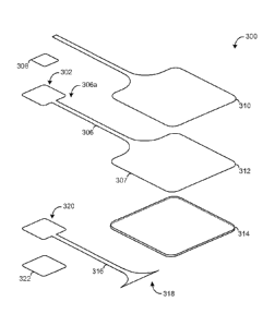
[00551 FIG. 3 is an exploded view of a unibody electrode 300. The electrode
300 includes
a nonconductive top layer 310 disposed along the top of a conductive layer 312
and a gel
layer 314 disposed beneath the conductive layer 312. The electrode 300 also
includes a
nonconductive bottom layer 316 with an extension portion 318 disposed
partially beneath the
conductive layer 312 and partially beneath the gel layer 314. The materials
and arrangements
of the nonconductive top layer 310, the conductive layer 312, the gel layer
314, and the
nonconductive bottom layer 316 arc as described above for the corresponding
components of
the unibody electrode 100 of FIG. 1. The conductive layer 312 also includes a
unitary
tail 306 which has at its distal end 306a a flared portion 302. The flared
portion 302, the
unitary tail 306 and the body 307 of the conductive layer 312 are formed from
a continuous
conductive material. The nonconductive bottom layer 316 also includes a flared
portion 320.
The flared portion 320 of the nonconductive bottom layer 316 may have
approximately the
same dimensions as the flared portion 302 of the unitary tail 306. In some
implementations,
the conductive layer 312 and the nonconductive bottom layer 316 are die cut to
have the same
dimensions.
[0056] FIG. 3 also illustrates a second conductive layer 308 disposed on the
flared
portion 302 of the distal end 306a of the unitary tail 306. In some
implementations the
second conductive layer 308 is formed from a different conductive material
than the
conductive layer 312. For example, the conductive layer 312 may be formed from
aluminum
and the second conductive layer 308 may be a carbon strip or a conductive
plastic such as a
conductive polyvinylchloride or a polyurethane impregnated with carbon. The
second
conductive layer 308 may provide additional stiffness to the flared portion
302 of the unitary
tail 306. In some implementations, the extra stiffening provided by the second
conductive
layer 308 allows the flared portion 302 to be formed by automated
manufacturing equipment
(e.g., conversion equipment) into a connector for the electrode 300, and may
increase the
mechanical strength of the resulting connector. Further description is
provided below of
-11-
CA 02841950 2014-01-14
WO 2013/012465 PCMJS2012/033575
representative (non-limiting) implementations connectors formed from the
flared portion 302.
FIG. 3 also illustrates a bottom support layer 322 which is formed from a
nonconductive
material and may be included in the electrode 300 instead of or in addition to
the flared
portion 320 of the nonconductive bottom layer 316 to provide mechanical
support.
[0057] FIGS. 4A-4C illustrate a connector 400 formed from the electrode 300
illustrated in
FIG. 3. FIG. 4A illustrates a nonconductive top layer 404 disposed on top of a
conductive
layer 406, forming an electrode tail 402 with a flared portion 408 located at
its distal end.
The flared portion 408 is an extension of the conductive layer 406 and has a
second
conductive layer 422 disposed thereon. The sides 420a and 420b of the flared
portion 408 are
curved toward one another, for example, using a mandrel or another suitable
manufacturing
process. FIG. 4B illustrates the tube 410 that is formed when the sides 420a
and 420b are
brought together. The sides 420a and 420b may be attached to one another by
sealing,
gluing, stapling, or may simply be overlapped. FIG. 4B also illustrates a
segment of heat-
shrink tubing 414. Once the sides 420a and 420b have been brought into
proximity, the heat-
shrink tubing 414 is positioned over the tube 410, extending onto the unitary
tail 406 beyond
the tube 410. When heat is applied, the heat-shrink tubing 414 will preferably
conform to the
unitary tail 406 and to the tube 410, as shown in FIG. 4C. Once the heat-
shrink tubing 414
has conformed to the tube 410, the heat-shrink tubing 414 provides mechanical
support for
the tube 410 and the unitary tail 406 and provides electrical insulation
between the tube 410
and a user of the electrode. The tube 410 forms an inner passageway 412 which
is configured
to receive a male pin from an electrostinaulation lead (not shown). The second
conductive
layer 422 on the flared portion 408 helps strengthen the connector 400 against
the wear and
tear of to connection and disconnection. The process of forming the connector
400 from the
flared portion 408 of the unitary tail of the conductive layer 406 may be
automated, further
improving the uniformity of the electrodes.
[0058] FIG. 5 is an exploded view of a snap electrode 500. The electrode 500
includes a
nonconductive top layer 502 with a first aperture 516, a conductive layer 504
with a second
aperture 518, and a gel layer 506. The materials and arrangements of the
nonconductive top
layer 502, the conductive layer 504, and the gel layer 506 are as described
above for the
corresponding components of the unibody electrodes 100 and 300 of FIGS. 1 and
3,
respectively. The snap electrode 500 further includes a first conductive
housing 508 and a
second housing 510 with a conductive post 511 that is anchored to the second
housing 512
and fits within a receptacle (not shown) of the first conductive housing 508
to join the two
housings 508 and 510. The second housing 510 includes a second conductive
housing 512
-12-
CA 02841950 2014-01-14
WO 2013/012465 PCMJS2012/033575
disposed beneath the conductive layer 504. The second conductive housing 510
also includes
a nonconductive element 514 disposed beneath the second conductive housing 512
and the
conductive layer 504 and above the gel layer 506. The second aperture 518 is
sized to
receive a portion of the second conductive housing 510. When the snap
electrode 500 is
assembled, the second housing 510 mates with the first conductive housing 508
to sandwich
the conductive layer 504 and the nonconductive top layer 502 with the post 511
extending
through the apertures 516 and 518 in the layers 502 and 504, respectively.
[00591 The nonconductive element 514 is formed from an insulating material,
such as a
dielectric polymer, and has perimeter dimensions that are equal to or greater
than the
footprint of the second conductive housing 512. In use, current from an
electrostimulation
device passes from an electrical lead (not shown) to the first conductive
housing 508, the
conductive layer 504, and the second conductive housing 512. The current is
then distributed
to a patient's tissue through the gel layer 506. The nonconductive element 514
forces current
to flow through the gel layer 506 around the nonconductive element 514,
preventing
.. excessive current from taking the path of least resistance from the second
conductive
housing 512 through the portion of the gel layer 506 directly beneath the
second conductive
housing 512 to the patient's tissue, and thereby preventing a buildup of heat
and current (a
"hotspot") directly below the first conductive housing 508 and the second
conductive
housing 512a. Conventional snap electrodes, which do not include a
nonconductive element
.. between a conductive layer and a gel layer, tend to form hotspots beneath
the snap connector
because of such direct current flow, which may burn a patient's tissue. The
electrode 500
reduces the likelihood of such hotspots by positioning a nonconductive barrier
within a path
from the second conductive housing 512 to the patient's tissue, resulting in a
more uniform
current distribution over the gel layer 506.
[0060] FIG. 6 is an exploded view of a snap electrode 650, having a
nonconductive top
layer 620 with a first aperture 622, a conductive layer 604 with a second
aperture 618, and a
gel layer 606. The materials and arrangements of the nonconductive top layer
620, the
conductive layer 604, and the gel layer 606 are as described above for the
electrodes
illustrated in FIGS. 1, 3 and 5. The snap electrode 650 further includes a
first conductive
housing 608 and a second housing 624. The second aperture 618 is sized to
receive a post
portion 613 of the second housing 624. When the snap electrode 650 is
assembled, the port
portion 613 of the second housing 624 mates with the first conductive housing
608 to span
the conductive layer 604 and the nonconductive top layer 620, as described
above with
reference to the electrode 500 of FIG. 5. The first conductive housing 608
makes electrical
-13-
CA 02841950 2014-01-14
WO 2013/012465 PCMJS2012/033575
contact with the conductive layer 604 through the aperture 622 in the
nonconductive top
layer 620.
[0061] The second housing 624 is formed from an electrically insulating
material, such as a
dielectric polymer. Like the snap electrode 500 of FIG. 5, the snap electrode
650 also
prevents the formation of a hotspot directly beneath the first conductive
housing 608. In use,
the nonconductive second housing 624 acts as a barrier to the direct flow of
current from the
first conductive housing 608 to the patient's tissue through the gel layer
606. The result is a
more uniform current distribution over the gel layer 606 and a reduced
likelihood of
dangerous hotspots.
[0062] FIGS. 7 and 8 illustrate magnetic connector electrodes. FIG. 7 is an
exploded view
of a magnetic connector electrode 700. The electrode 700 includes a socket
712, a
nonconductive top layer 706 with an aperture 708, a conductive magnetic layer
704, a
conductive layer 702 and a gel layer 722. The materials and arrangements of
the
nonconductive top layer 706, the conductive layer 702, and the gel layer 722
are as described
above for the electrodes illustrated in FIGS. 1, 3, 5 and 6. The socket 712 is
formed from a
rigid nonconductive material such as a plastic and may be bonded, glued or
otherwise affixed
to the top of the nonconductive top layer 706. The conductive magnetic layer
704 is
positioned below the aperture 708 of the nonconductive top layer 706. The
conductive
magnetic layer 704 may be formed from a ferritic material, such as a stainless
steel, but may
be any conductive magnetic material. The conductive layer 702 may be formed
from any
conductive material such as aluminum. The conductive magnetic layer 704 is
positioned
between the nonconductive top layer 706 and the conductive layer 702. An
adhesive on the
bottom surface of the nonconductive top layer 706 sandwiches the conductive
magnetic
layer 704 between the nonconductive top layer 706 and the conductive layer 702
thereby
holding the conductive magnetic layer 704 in place when the magnetic connector
electrode 700 is assembled.
[0063] FIG. 8 is an exploded view of a magnetic connector electrode 850. The
electrode 850 includes a nonconductive top layer 820, with an aperture 810, a
socket 814, a
conductive magnetic layer 804, a conductive layer 802 and a gel layer 822.
Unlike the
magnetic connector electrode 700 of FIG. 7, the magnetic connector electrode
850 of FIG. 8
has the socket 814 positioned below the nonconductive top layer 820. The
particular
implementation of the socket 814 shown in FIG. 8 has a top portion 816 and a
bottom
portion 818 wherein the diameter of the top portion 816 is smaller than the
diameter of the
bottom portion 818 and the sides of the socket 814 flare between the top
portion 816 and the
-14-
CA 02841950 2014-01-14
WO 2013/012465 PCMJS2012/033575
bottom portion 818. When the electrode 850 is assembled, the top portion 816
of the
socket 814 protrudes through the aperture 810 in the nonconductive top layer
820 while the
bottom portion 818 of the socket 814 remains below the nonconductive top layer
820. The
conductive magnetic layer 804 is disposed under the socket 814. Both the
socket 814 and the
conductive magnetic layer 804 are sandwiched between the nonconductive top
layer 820 and
the conductive layer 802, for example, using an adhesive bond between the
nonconductive
top layer 820 and the conductive layer 802.
[00641 The magnetic connector electrodes of FIGS. 7 and 8 provide one or more
of a
number of advantageous features. First, the use of a magnetic connection
mechanism
achieves smoother vertical connection and disconnection compared to snap
connection
mechanisms which require the patient or clinician to overcome a resistive
mechanical force in
order to connect or disconnect an electrode. This makes it easier for
arthritic or impaired
users to connect and disconnect the electrodes and also avoids applying a
jarring force to
damaged or sensitive tissue. Second, because the conductive magnetic layer
(layer 704 of
FIG. 7 and layer 804 of FIG. 8) is attracted to the magnet included in a
magnetic lead
connector (such as the magnetic lead connector 904 of FIG. 9), the magnetic
connector
electrodes of FIGS. 7 and 8 are easier for users to apply and connect in
places on the body
that are difficult to see, such as the back. Third, the sockets 712 and 814
help a patient or
clinician position a magnetic lead connector (such as the magnetic lead
connector 902
depicted in FIG. 9) so that the magnetic lead connector is aligned with the
conductive
magnetic layer (layer 704 of FIG. 7 and layer 804 of FIG. 8) to achieve
magnetic coupling
sufficient to hold the magnetic lead connector to the electrode. In some
implementations, the
shape of the socket (such as socket 712 or 814) may be selected so that only
magnetic lead
connectors of a complementary shape can be seated within the socket (referred
to as "keying"
the connector to the socket). Keying of the socket and connector allows
manufacturers to
create magnetic lead connector/electrode combinations that are designed to
work together and
prevents the use of other magnetic lead connector/electrode combinations that
may not be as
therapeutically beneficial. Fourth, the sockets 712 and 814 provide a
mechanical barrier that
prevents a magnetic lead connector from being disconnected from the electrode
by a lateral
force (such as a tug on the lead wire 908 shown in FIG. 9). Clinically,
lateral pulls account
for a significant percentage of disconnection events; since the magnetic force
between the
conductive magnetic layer (layer 704 of FIG. 7 and layer 804 of FIG. 8) and a
magnet
included in a magnetic lead connector is weaker in the lateral direction than
in the vertical
direction, the sockets 712 and 814 provide additional security against such
pulls.
-15-
CA 02841950 2014-01-14
WO 2013/012465 PCMJS2012/033575
[0065] FIG. 9 illustrates a magnetic lead connector 902 that may be used to
mate a lead
wire 908 from an electrostimulation device (not shown) to either of the
magnetic connector
electrodes of FIGS. 7 and 8. The magnetic lead connector 902 includes a
connector base
portion 912 upon which a magnet 904 is mounted. The magnet 904 is made from a
conductive material, such as neodymium, and is electrically connected to the
lead wire 908.
In some implementations, the magnet 904 is soldered to the lead wire 908 or an
intermediate
conducting element (not shown); in such implementations, the magnet 904 is
preferably kept
cool to avoid changing the crystalline structure of the magnet 904 and
affecting its magnetic
properties. In some implementations, the magnet 904 is held to the connector
base
portion 912 using a metal claw system that includes a formed female receiver
that friction fits
with the magnet 904. In some implementations, a glue (such as a conductive
glue) may be
used to attach the magnet 904 to the connector base portion 912. The magnetic
lead
connector 902 of FIG. 9 also includes an outer wall 906 which may be formed
from a
nonconductive material and may be configured to surround a socket of an
electrode (such as
the socket 712 of FIG. 7 or the top portion 816 of the socket 814 of FIG. 8
when the magnetic
lead connector 902 is mated to the electrodes illustrated in the respective
figures). The outer
wall 906 may provide additional pull strength that prevents the magnetic lead
connector 902
from being displaced from connection with either a magnetic connector
electrode by a
laterally applied force, such as a lateral tug on the lead wire 908. In some
implementations of
the magnetic lead connector 902, no outer wall is included. When the magnetic
lead
connector 902 is attached to the electrode 700 of FIG. 7 or the electrode 850
of FIG. 8, the
magnet 904 seats within the socket 712 or 814, respectively, and provides an
electrical
connection between the magnet 904 and conductive magnetic layer (layer 704 of
FIG. 7 and
layer 804 of FIG. 8). In use, electrostimulation current passes from an
electrostimulation
current generator (not shown) through the lead wire 908, through the magnet
904, through the
conductive magnetic layer, to the conductive layer (layer 702 of FIG. 7 and
layer 802 of
FIG. 8), and through the gel layer (layer 722 of FIG. 7 and layer 822 of FIG.
8) to a patient's
tissue.
[0066] FIGS. 10A and 10B illustrate an inverted snap electrode 1000 which may
be formed
in accordance with the unibody electrode construction techniques described
herein. FIG. 10A
is an exploded view of the inverted snap electrode 1000. The inverted snap
electrode 1000
includes a nonconductive top layer 1002 with an aperture 1004 encircled by a
reinforcing
ring 1006 disposed above or within the nonconductive top layer 1002. The
reinforcing
ring 1006 is comprised of a nonconductive material (e.g., any of the materials
described
-16-
CA 02841950 2014-01-14
WO 2013/012465 PCMJS2012/033575
herein as suitable for use in a nonconductive or insulating layer), and may
provide
mechanical reinforcement to the inverted snap electrode 1000 when a snap
connector is
connected and disconnected from the inverted snap electrode 1000 during use.
The inverted
snap electrode also includes a conductive layer 1008 with a depression 1010,
and a gel
layer 1016 with a depression 1018. The materials of the nonconductive top
layer 1002, the
conductive layer 1008, and the gel layer 1016 are as described above for the
corresponding
components of the unibody electrodes 100 and 300 of FIGS. 1 and 3,
respectively. A
nonconductive element 1014 is positioned between the depression 1010 of the
conductive
layer 1008 and the depression 1018 of the gel layer 1016. FIG. 10B is a cross-
sectional view
of the inverted snap electrode of FIG. 10A, including the nonconductive top
layer 1002, the
conductive layer 1008 and the depression 1010, the gel layer 1016 and the
depression 1018,
and the nonconductive element 1014.
[0067] The depression 1010 of the conductive layer 1008 may be mechanically
formed in
any of a number of ways, such as vacuum forming or thermoforming during a roll
manufacturing process. The depression 1010 is formed as a female receptacle to
receive a
male connector (e.g., the male portion 1102 of the connector 1100 of FIG. 11,
described in
detail below) within the conductive layer 1008. In some implementations, the
depression 1010 is dimensioned to snugly receive a standard male snap
connector. In some
implementations, the depression 1010 is dimensioned to snugly receive a custom-
sized or
custom-shaped male connector. A custom male connector may have any depth,
width, length
or shape, and may act as a "keyed" connector in that only connectors whose
shape is
complementary to the receptacle formed by the depression 1010 can securely
mate with the
inverted snap electrode 1000. The use of a keyed connector with the inverted
snap
electrode 1000 (or any of the electrodes and electrode systems described
herein) may
improve therapeutic outcomes by reducing the likelihood that the wrong
electrode (of a
family of keyed electrodes) will be used with a given electrotherapy device or
that low-
quality electrodes manufactured without approval of the electrotherapy device
manufacturer
can successfully mate with the keyed connector.
[0068] During certain modes of assembly, the nonconductive element 1014 is
positioned
beneath the bottom surface of the depression 1010 of the conductive layer
1008, between the
conductive layer 1008 and the gel layer 1016. The depression 1018 of the gel
layer 1016 is
complementary to the profile of the depression 1010 and the nonconductive
element 1014,
but preferably does not extend past the bottom surface of the gel layer 1016
so that a flat gel
surface may be applied to the patient's tissue. In a preferred implementation,
the gel
-17-
CA 02841950 2014-01-14
WO 2013/012465 PCMJS2012/033575
layer 1016 is poured onto the conductive layer 1008 after the depression 1010
has already
been formed and the nonconductive element 1014 positioned, after which the gel
layer 1016
is cross-linked in place (referred to as a "pour-in-place" process). The gel
layer 1016 and its
depression 1018 could also be formed in a mold, either individually or in
sheets. As
discussed above with reference to the nonconductive element 514 of FIG. 5, the
nonconductive element 1014 forces current to flow through the gel layer 1016
around the
nonconductive element 1014, preventing excessive current from taking the path
of least
resistance from the depression 1010 of the conductive layer 1008 through the
portion of the
gel layer 1016 directly beneath the depression 1010 to the patient's tissue,
and thereby
preventing a ''hotspot" from forming below the depression 1010.
[0069] The inverted snap electrode 1000 may have advantages over standard snap
electrodes. First, by including a female receptacle within the electrode
itself (instead of in the
connector, as is typical in snap-electrode-based systems), and thereby lodging
in the depth of
the male connector within the thickness of the electrode (rather than above
the surface of the
electrode as in most available systems), the inverted snap electrode 1000
provides a lower
profile than existing snap electrode systems. This lower profile allows the
inverted snap
electrode 1000 to be used in therapeutic settings in which existing snap
electrodes are
unsuitable, such as within a cast or brace. The low profile of the inverted
snap
electrode 1000 also reduces the likelihood that the electrode or connector
will catch on a
patient's clothing or other objects as the patient is moving, and thus may be
better suited for
electrostimulation or monitoring of active patients (e.g., during sports
therapy) than existing
electrodes. The inverted snap electrode 1000 may also be easier to use than
traditional "low
profile" electrodes in which a small lead pin must be fed into a socket at the
end of the
electrode's lead wire. This may particularly benefit older patients, who
typically find snap
.. electrodes easier to use than the lead pin embodiments. Additionally,
manufacturing
advantages may be achieved by using a roll material (such as an aluminum
laminate) to form
the conductive layer 1008, or by using a pour-in-place process for adding the
gel layer 1016.
In some implementations, the inverted snap electrode 1000 may be manufactured
using
automated conversion equipment, which may result in improved efficiency,
reliability and
uniformity as compared to electrodes assembled by hand or by machines in which
material
must be manually transferred and loaded at multiple stages during
manufacturing.
[0070] FIG. 11 is a perspective view of' a connector 1100 that is configured
to mate a lead
wire 1106 with an inverted snap electrode such as the inverted snap electrode
1000 of
FIG. 10. The connector 100 includes a connector base portion 1104 upon which a
male
-18-
CA 02841950 2014-01-14
WO 2013/012465 PCMJS2012/033575
portion 1102 is disposed. The male portion 1102 is made from a conductive
material and is
electrically connected to the lead wire 1106. In some implementations, the
male portion 1102
is formed using a same or similar manufacturing technique as discussed above
to form the
depression 1010 in the conductive layer 1008 of the inverted snap electrode
1000 (e.g.,
vacuum or thermoforming), and may be formed from the same or a similar
material as the
conductive layer 1008. As shown, the male portion 1102 extends from the
connector base
portion 1104 through an aperture 1110 in a nonconductive top layer 1108. The
surface of the
nonconductive top layer 1108 that faces the connector base portion 1104 may be
adhesive,
and may mechanically capture the male portion 1102 between the nonconductive
top
layer 1108 and the connector base portion. In some implementations, no
nonconductive top
layer 1108 is included in the connector for the inverted snap electrode 1000,
and the male
portion 1102 is fastened to the connector base portion 1104 using an adhesive,
tabs, or other
fastener. When the lead connector 1100 is attached to the inverted snap
electrode 1000 of
FIG. 10, the male portion 1102 scats within the receptacle formed by the
depression 1010 and
provides an electrical connection between the lead wire 1106 and the
conductive layer 1108.
In use, electrostimulation current passes from an electrostimulation current
generator (not
shown), through the lead wire 1106, to the conductive layer 1108, and then to
a patient's
tissue. As discussed above with reference to FIG. 10, when the connector 1100
is mated with
the inverted snap electrode 1000, the two together may have a lower profile
than existing
snap electrode-connector assemblies, which may result in improved performance
and wider
use in different therapeutic and diagnostic environments.
[0071] Additional variations in electrode design are possible. For example,
FIG. 12 is an
exploded view of an electrode system 1200 that includes a plurality of
electrode structures,
similar to the unitary body and tail structures described above. The electrode
system 1200
includes a nonconductive top layer 1202, a first electrode 1204, an insulating
layer 1206, a
second electrode 1208 and a gel layer 1210. The first electrode 1204 and the
second
electrode 1208 are constructed from a unitary conductive material, as
discussed above with
reference to FIGS. 1 and 3. The first electrode 1204 includes a unitary tail
1222 and a
body 1224. The insulating layer 1206 includes a hole 1214 that is sized to
approximately
match the outer diameter of' the body 1224 of the first electrode 1204. The
second
electrode 1208 includes a unitary tail 1220 and a body 1221. The body 1221 of
the second
electrode 1208 includes a hole 1212 sized to approximately match the outer
dimensions of the
insulating layer 1206. The gel layer 1210 includes a first gel segment 1210a
and a second gel
segment 1210b. The first gel segment 1210a is sized to approximately match the
dimensions
-19-
CA 02841950 2014-01-14
WO 2013/012465 PCMJS2012/033575
of the body 1221 of the second electrode 1208 and the second gel segment 1210b
is sized to
approximately match the dimensions of the body 1224 of the first electrode
1204. The
nonconductive top layer 1202 may have outer dimensions that approximately
match the outer
dimension of the body 1221 of the second electrode 1208. The bottom surface of
the
nonconductive top layer 1202 may be coated with an adhesive to which the first
electrode 1204, the insulating layer 1206 and the second electrode 1208 may be
affixed.
When these components are affixed to the nonconductive top layer 1202, the
thickness of the
insulating layer 1206 may extend below a bottom surface of the second
electrode 1208, such
that when the first gel segment 1210a and the second gel segment 1210b are
affixed to the
bottom of the assembly, the bottom of the insulating layer 1206 may be in
approximately the
same plane as the bottom of the gel layer 1210, thereby presenting a
substantially uniform
surface to be affixed to the tissue of a patient.
[0072] FIG. 13 is an exploded view of an electrode system 1300 constructed in
accordance
with the description of the electrode system 1200 of FIG. 12. The electrode
system 1300
includes a nonconductive top layer 1302, a first electrode 1304, an insulating
layer 1306, a
second electrode 1308 and a gel layer 1310. The first electrode 1304 and the
second
electrode 1308 are constructed from a unitary conductive material, as
discussed above with
reference to FIGS. 1,3 and 12. The first electrode 1304 includes a unitary
tail 1322, a
body 1324, and a hole 1316. The insulating layer 1306 includes a hole 1314
that is sized to
approximately match the outer dimensions of the body 1324 of the first
electrode 1304. The
second electrode 1308 includes a unitary tail 1320 and a body 1321 with a hole
1312 that is
sized to approximately match the outer dimensions of the insulating layer
1306. The gel
layer 1310 includes a first gel segment 1310a and a second gel segment 1310b.
The
dimensions of the gel segment 1310a are sized to approximately match the
dimensions of the
body 1321 of the second electrode 1308 and the dimensions of the gel segment
1310b are
sized to approximately match the dimensions of the body 1324 of the first
electrode 1304.
[0073] FIG. 14 is an exploded view of an electrode system 1400. The electrode
system 1400 includes a nonconductive top layer 1404 with a hole 1406. The
electrode
system 1400 further includes a plurality of conductive zones 1402a, 1402b,
1402c and 1402d
mounted or printed on a substrate 1412. The substrate 1412 includes a tail
portion 1414 with
conductive traces 1422 to each of the conductive zones 1402. The substrate
1412 further
includes a hole 1408. The electrode system 1400 also includes an insulating
layer 1416 that
has a plurality of apertures 1418a, 1418b, 1418c and 1418d. Each of the
apertures 1418 is
positioned to align with a respective conductive zone 1402. The insulating
layer 1416 further
-20-
CA 02841950 2014-01-14
WO 2013/012465 PCMJS2012/033575
includes a hole 1410 that is coaxially aligned with the hole 1408 and the hole
1406. The
electrode system 1400 also includes a gel layer 1422 which has a plurality of
gel
segments 1420a, 1420b, 1420c and 1420d. When the electrode system 1400 is
assembled,
each of the gel segments 1420 is positioned within the respective apertures
1418 of the
insulating layer 1416. When the electrode system 1400 is in use, the gel
segments 1420 are
interposed between the conductive zones 1402 and the patient's tissue.
[0074] The electrode system 1400 is compatible with two-channel interferential
electrostimulation and TENS therapy, among others. The hole in the center of
the electrode
system 1400 provides a working area for clinicians who would like to
anesthetize a patient's
.. tissue in preparation for or during another medical procedure, such as
suturing or a needle
stick for drug delivery or testing. The hole also makes it easier to position
properly the
electrode on a patient's tissue: the patient or clinician can "center" the
hole over the site of
the patient's pain without having to separately position each conductive zone
separately.
Additionally, the ease of use of the electrode system 1400 provides an
advantageous way to
demonstrate the therapeutic effects of electrotherapy to patients who may
benefit from its
use: the electrode system 1400 and electrostimulation can be applied to a
patient's tissue
quickly, resulting in a demonstrable effect within a matter of seconds.
[0075] FIGS. 15A and 15B are front and back plan views, respectively, of a
connection
system that may be used to electrically connect conductive traces on an
electrode tail (such as
the conductive traces 1422 on the tail 1414 of the electrode system 1400 of
FIG. 14) to
separate connecting elements. In FIG. 15A, the tail 1414 is shown with four
conductive
portions 1422. Each of these conductive portions is pierced by a set of first
teeth 1502 and a
set of second teeth 1504 with the first and second teeth mounted respectively
on a plurality of
connectors 1506. The connectors 1506, including the first and second teeth
1502 and 1506
are formed from a conductive material, and can be attached to wire or other
conducting leads
to electrically connect an electrode system (such as the electrode system 1400
of FIG. 14) to
an electrostimulation device (not shown). FIG. 15B is a back view of the tail
1414 with the
connectors 1506 attached to the conductive portions 1422.
[0076] FIG. 16 is a perspective view of' a custom-cut electrode 1600
positioned on a
patient's finger 1602. In some implementations, the unibody electrodes
described herein
(which include an electrode body and an electrode tail formed integrally from
a continuous
piece of conductive material) can be cut by a clinician or patient to fit the
particular contours
of a patient's tissue. For example, a clinician can use a standard pair of
scissors to cut the
electrode 1600 of FIG. 16 from a larger electrode (e.g., the electrodes of
FIGS. 1 and 3) to fit
-21-
CA 02841950 2014-01-14
WO 2013/012465 PCMJS2012/033575
a treatment area on a patient's finger 1602. Conventional electrodes, which
include a multi-
strand tail fanned to form various contact points on a conductive polymer,
cannot be cut in
this fashion with risking damage to the fanned strands. The electrodes
described herein
improve the delivery of electrostimulation by allowing clinicians to customize
the shape and
size of an electrode to a patient's unique contours and treatment goals.
[0077] FIGS. 17 and 18 are plan views of two ribbon electrodes 1700 and 1800.
respectively. Each of these electrodes includes a conductive layer with an
integrally formed
tail. In some implementations, the dimensions of the body of the electrodes
1700 and 1800
are approximately 3/4" by 5", though any other dimensions may be used. The
tail 1702 of the
electrode 1700 of FIG. 17 is oriented longitudinally with respect to the
primary axis of the
electrode 1700, while the tail 1802 of the electrode 1800 of FIG. 18 is
oriented
perpendicularly with respect to the primary axis of the electrode 1800. Ribbon
electrodes
such as these may be wrapped around a portion of a patient's body, such as a
wrist or knee.
The unitary construction techniques described herein allow the fabrication of
electrodes with
extended shapes, such as the ribbon electrodes 1700 and 1800, without risking
dissimilar
metal corrosion or hotspots resulting from fanned metal connections.
[0078] FIG. 19A is a cross-sectional view of a portion of an electrode body
1900 (which
may be used with any of the electrodes described herein). A nonconductive top
layer 1904 is
disposed above a conductive layer 1906 to cover the conductive layer 1906.
Additional
conductive and nonconductive layers may also be included in the electrode body
1900 (or any
other electrode body) but are not shown in FIG. 19A for ease of illustration.
A gel layer 1908
is disposed below the conductive layer 1906 and a gel coating 1910 contiguous
with the gel
layer 1908 extends around the side of the body 1900 to cover the perimeter
side
surfaces 1902 of the conductive layer 1906. The presence of the gel coating
1910 on the
perimeter side surfaces 1902 helps prevent electrical current from bypassing
the gel
coating 1910 or the gel layer 1908 and entering a patient's or clinician's
tissue directly, which
could cause a painful shock or an uneven distribution of current. The
configuration of the gel
coating 1910 depicted in FIG. 19A may be achieved by die cutting electrodes
from layers of
material, for example.
[0079] FIG. 19B is a cross-sectional view of an electrode tail 1920 (which may
be used
with any of the electrodes described herein, for example, as a unitary
extension of an
electrode body). The electrode tail 1920 includes a nonconductive top layer
1922, a
conductive layer 1924 and a nonconductive bottom layer 1926. Additional
conductive and
nonconductive layers may also be included in the electrode tail 1920, but are
not shown in
-22-
CA 02841950 2014-01-14
WO 2013/012465 PCMJS2012/033575
FIG. 19B for ease of illustration. The electrode tail 1920 also has left
perimeter side
surface 1928a and right perimeter side surface 1928b. An insulating coating
1930 is disposed
along the perimeter side surfaces 1928 to help prevent inadvertent electrical
contact between
a patient or clinician and the conductive layer 1924 along the sides of the
electrode tail 1920,
or between the conductive layer 1924 and another electrically-exposed surface
(such as the
tail of another electrode). As shown, the insulating coating 1930 has a left
coating area 1930a
that covers the left perimeter side surface 1928a and a right coating area
1930b that covers
the right perimeter side surface 1928b. In some implementations, the
insulating coating 1930
is a silicone applied in liquid form.
.. [0080] Automated manufacturing processes may be used to form the electrodes
described
herein. In some implementations, electrodes are formed with rotary conversion
machinery,
which fabricates electrodes from roll stock by dispensing adhesive,
laminating, and cutting,
among other operations. A second automated manufacturing process may be used
to form a
connector (such as the connector 400 formed from the flared portion 408 of a
unitary
conductive tail 406 depicted in FIGS. 4A-4C) or attach a connector (such as
the connector
housing 120 with the undulating receptacle 122 depicted in FIGS. 2A-2B, or the
connectors 1506 depicted in FIGS. 15A-15B).
[0081] FIG. 20A is an exploded view of a stimulation system 2000 with an
electronics
layer 2012. Like the electrode system 1200 of FIG. 12, the stimulation system
2000 includes
.. a plurality of electrode structures. In particular, the stimulation system
2000 includes a
nonconductive top layer 2002, a first electrode 2004, an insulating layer
2006, a second
electrode 2008 and a gel layer 2010 having a first gel segment 2010a and a
second gel
segment 2010b of a gel layer 2010. The first electrode 2004 and the second
electrode 2008
are constructed as described above with reference to the corresponding
structures of FIG 12,
as are the nonconductive top layer 2002, the insulating layer 2006 and the gel
layer 2010.
Unlike the electrode system 1200 of FIG. 12, the stimulation system 2000
includes an
electronics layer 2012 disposed below the nonconductive top layer 2002 and the
first
electrode 2004. A nonconductive layer 2026 is disposed between the electronics
layer 2012
and the first electrode 2004; in some implementations, the nonconductive layer
2026 takes
the form of a coating of a nonconductive material (such as a nonconductive
plastic) on the
bottom surface of the electronics layer 2012 or the top surface of the first
electrode 2004.
[0082] The electronics layer 2012 includes circuitry for performing one or
more
electrostimulation treatments. In some implementations, the electronics layer
2012 includes a
printed circuit board configured with passive and active electrical components
to perform a
-23-
CA 02841950 2014-01-14
WO 2013/012465 PCMJS2012/033575
predetermined or programmable electrostimulation protocol. These electrical
components
may include one or more control microprocessors configured with machine-
executable logic
to control the conversion of energy from one or more power supplies included
in the
electronics layer 2012 (such as printed or coin cell batteries) into
electrostimulation currents
that may be driven into a patient's tissue through one or both of the first
electrode 2004 and
the second electrode 2008. The electronics layer 2012 may include printed
traces of an
electrically conductive material on one or more sub-layers (not shown) that
connect the
circuit components. Among the circuit components included in the electronics
layer 2012 is
a pulse generator 2024. The pulse generator 2024 generates two different
channels of
electrical signals that are transmitted to a patient's tissue via the first
electrode 2004 and the
second electrode 2008, respectively. Various illustrative implementations of
pulse generators
are described below with reference to FIGS. 21-24.
[0083] In the stimulation system 2000, the electronics layer 2012 is
electrically connected
to the first electrode 2004 via contact points 2014a (in the electronics layer
2012) and 2016a
(in the first electrode 2004). These contact points 2014a and 2016a are
electrically connected
by a puncture technique, in which the contact point 2014a of the electronics
layer 2012 is
aligned with and positioned adjacent to the contact point 2016a of the first
electrode 2004,
and the electronics layer 2012 and the first electrode 2004 are punctured at
the contact
points 2014a and 2016a to form an electrical connection between conductive
materials
included in the electronics layer 2012 and the first electrode 2004. In some
implementations,
the puncture connections are folioed by pushing a pin, rod, or other rigid
member through a
conductive portion of the electronics layer 2012 to deform the conductive
portion and form a
hole surrounded by protrusions of the conductive material extending away from
the
electronics layer 2012. In some implementations, these protrusions are jagged
and irregular,
while in other implementations, the body of the conductive layer is pre-scored
or otherwise
prepared so that the protrusions are more regularly spaced and sized. When the
electronics
layer 2012 is separated from the first electrode 2004 by the nonconductive
layer 2026, the
protrusions extend through the nonconductive layer 2026 and can be bent to
fold back against
the first electrode 2004 to form an electrical connection between the
conductive portion of the
electronics layer 2012 and the first electrode 2004. In some implementations,
the electronics
layer 2012, the nonconductive layer 2026 and the first electrode 2004 are
stacked, and the
puncturing operation is applied to the entire stack.
[0084] Because the electronics layer 2012 is separated from the first
electrode 2004 at all
points other than the puncture locations by the nonconductive layer 2026, the
puncture
-24-
CA 02841950 2014-01-14
WO 2013/012465 PCMJS2012/033575
between the contact points 2014a and 2016a will allow electrical signals
generated by an
appropriate channel of the pulse generator 2024 (e.g., a first channel) to
flow to the first
electrode 2004 without short-circuiting the remaining components in the
electronics
layer 2012. Although only one contact point between the electronics layer 2012
and the first
electrode 2004 is shown in FIG. 20, any number of contact points may be used.
The
stimulation system 2000 also includes a nonconductive element 2018a positioned
below the
contact point 2016a, which may prevent the formation of hotspots within the
gel layer 2010
as discussed above.
[0085] One or more sets of similar contact points may be provided. As shown in
FIG. 20A,
a second set of contact points 2014b and 2016b is included in the electronics
layer 2012 and
the second electrode 2008, respectively. The electrical signals generated on a
second channel
of the pulse generator 2024 are transmitted to the second electrode 2008. The
contact
points 2014b and 2016b are connected using the puncture technique described
above. The
stimulation system 2000 also includes a nonconductive element 2018b positioned
below the
contact point 2016b. FIG. 20B is a cross-sectional view of the stimulation
system of
FIG. 20A. Although two electrodes and a single electronics layer are
illustrated in FIG. 20,
any number of electrodes and any number of electronics layers, arranged in any
desired
orientation, may be used (such as any of the electrode systems described
herein). Using this
connection structure, different output channels of the pulse generator 2024
may be directed to
different electrodes within the stimulation system 2000 without the use of
bulky wires or the
need for hand-soldering. In some implementations, the puncture connections are
formed by
rotary converting equipment acting on rolls of material that provide the
electronics
layer 2012, the first and second electrodes 2004 and 2008, respectively, and
the
nonconductive layer 2026. Automation of the puncture connection process, as
well as other
steps in the production of the electrodes and systems described herein, may
enable the
effective fabrication of previously infeasible structures and may improve the
quality of the
manufactured items. For example, an automated electrode manufacturing process
may be
more readily monitored (e.g., using cameras and other sensors) than a manual
assembly
process, which may enable earlier detection of manufacturing errors thereby
preventing
unsuitable electrodes from entering the marketplace.
[0086] The electronics layer 2012 also includes the electrical switches 2022a,
2022b
and 2022c. These electrical switches are components that provide an electrical
response to
forces exerted on the surface of the switches, and are commonly used in user
interface design
for registering button presses or other user inputs. Three buttons 2020a,
2020b and 2020c are
-25-
disposed above the electrical switches 2022a, 2022b and 2022c, respectively,
and are aligned
with the apertures 2018a, 2018b and 2018c, respectively, in the nonconductive
top layer
2002. The electrical switches 2022a, 2022b and 2022c are in electrical
communication with a
microprocessor or other circuitry included in the electronics layer 2012 and
are used to
initiate or adjust the electrostimulation provided by the stimulation system
2000. As shown in
FIG. 20A, the power button 2020b, marked "ON," may be pressed by a user or
clinician to
activate the power switch 2022b to initiate (and possibly to terminate) an
electrostimulation
treatment. The buttons 2020a and 2020c are marked with "+" and "2 symbols,
respectively,
to indicate that a patient or clinician may use those buttons to activate the
intensity
adjustment switches 2022a and 2022c to adjust up and down, respectively, the
intensity of
the electrostimulation provided by the stimulation system 2000 (e.g., changing
the amplitude
or frequency of a generated stimulation current). Additional user interfaces
that may be
implemented instead of or in addition to the keys 2020a, 2020b and 2020c are
described in
Mueller et al., U.S. Patent Application Publication No. 2010/0042180.
-26-
CA 2841950 2018-05-29
100871 The circuitry included in the electronics layer 2012 of the
stimulation system 2000
may be configured to generate one or more electrostimulation protocols (i.e.,
a predefined
current or voltage waveform). These electrostimulation protocols may be stored
in a memory
(such as an EEPROM) included in the electronics layer 2012, or may be encoded
into the
circuitry using logic gates or other circuitry (e.g, an ASIC). In some
implementations, the
stimulation system 2000 is configured to provide a single electrostimulation
protocol when
the power button 2020b is pressed (e.g., a particular TENS therapy or a
particular
iontophoretic treatment). The single electrostimulation protocol may be
directed to treating a
particular condition (e.g., pain or muscle tension), and the stimulation
system 2000 may be
packaged and provided to clinicians and patients as a treatment for the
particular condition
along with instructions on how to position to stimulation system 2000 on the
patient's tissue.
The stimulation system 2000 can then be activated and the electrical treatment
delivered by
depressing the power button 2020b. In some implementations, the stimulation
system 2000
can only be used a predetermined number of times before the stimulation system
2000 will
.. no longer respond to presses of the power button 2020b. The number of times
that the
stimulation system 2000 has been turned on may be stored in an EEPROM or other
memory
included in the electronics layer 2012, and a microprocessor may be configured
to count up
or down to a fixed value that represents the maximum number of uses. In some
implementations, the electrostimulation protocols may provide for
electrostimulation
-26a-
CA 2841950 2018-05-29
CA 02841950 2014-01-14
WO 2013/012465 PCMJS2012/033575
treatment over a predetermined period of time (e.g., thirty minutes). The time
period may be
enforced by timer circuitry included in the electronics layer 2012, or by a
chemical or other
switch in the electronics layer 2012.
[0088] In some implementations, the circuitry included in the electronics
layer 2012 of the
stimulation system 2000 may be configured to provide an iontophoretic
treatment followed
by a TENS treatment. In such implementations, the gel segments 2010a and 2010b
are
replaced with drug delivery reservoirs that contain charged compounds that are
drive from
the reservoirs into a patient's skin when a DC current is applied via the
first and second
electrodes 2004 and 2008. The drug delivery reservoirs may contain, for
example, a drug
delivery matrix in which the therapeutic compounds are suspended.
[0089] FIG. 21 is a flow diagram illustrating the operation of a stimulation
system (such as
the stimulation system 2000 of FIG. 20) configured to deliver iontophoretic
and TENS
therapy. At step 2102, the stimulation system 2000 delivers an iontophoretic
treatment by
applying an electric field to drive a therapeutic compound into the patient's
tissue. When the
stimulation system 2000 detects that the iontophoretic treatment time has
elapsed at
step 2104, the stimulation system 2000 begins to deliver a TENS treatment. As
discussed
above, the stimulation system 2000 may determined that the iontophoretic
treatment time has
elapsed at step 2104 using timer circuitry included in the electronics layer
2012, or by a
chemical or other switch in the electronics layer 2012.
[0090] The delivery of the iontophoretic treatment and the TENS treatment may
take place
using the same sets of electrodes (i.e., the first electrode 2004 and the
second electrode 2008),
but by applying different waveforms to those electrodes. FIG. 22 depicts an
illustrative
waveform 2200 generated by the stimulation system 2000 to provide
iontophoretic treatment
during a first portion 2200a of the waveform 2200 and a TENS treatment during
a second
portion 2200b of the waveform 2200. The first portion 2200a is a DC portion,
representing
the one-way flow of current between the first electrode 2004 and the second
electrode 2008
over the time period T1. The first portion 2200a of the waveform 2200 provides
the electric
field that drives the therapeutic compound into the patient's tissue. The
iontophoretic
treatment is illustrated in FIG. 23A, in which current is applied in one
direction (indicated by
the arrows 2310) between the first electrode 2004 (and its corresponding
reservoir 2302) and
the second electrode 2008 (and its corresponding reservoir 2304) through the
patient's
tissue 2308. As a result, the therapeutic compound 2306 is driven into the
patient's
tissue 2308.
-27-
CA 02841950 2014-01-14
WO 2013/012465 PCMJS2012/033575
[0091] When the stimulation system 2000 determines that the iontophoretic
treatment time
has ended (represented with the vertical line 2202 in FIG. 22), the circuitry
included in the
electronics layer 2012 of the stimulation system 2000 begins to generate an AC
waveform.
In some implementations, this circuitry includes an H-bridge transistor
configuration. The
.. second portion 2200b shown in FIG. 22 is a square, biphasic, symmetric
waveform, but other
AC waveforms may also be used. The TENS treatment is illustrated in FIG. 23B,
in which
current is applied in two directions (indicated by the arrows 2310 and 2312)
between the first
electrode 2004 (and its corresponding reservoir 2302) and the second electrode
2008 (and its
corresponding reservoir 2304) through the patient's tissue 2308. In preferred
.. implementations, the TENS portion of the waveform has no DC component so
that the
stimulation system does not transfer any therapeutic compound remaining in the
reservoirs
after the iontophoretic treatment time has been reached. Additionally, the
presence of
residual compound may improve the conductivity of the interface between the
electrodes of
the stimulation system and the patient's tissue.
.. [0092] In preferred implementations, the same power source (e.g., a
battery) that provides
the energy for the iontophoretic treatment (at step 2012 of FIG. 21) is used
to provide the
energy for the TENS treatment (at step 2106 of FIG. 21). In some existing
iontophoretic
devices, additional battery power may remain after the iontophoretic treatment
is complete;
when these devices are disposable, the batteries are thrown away and this
energy is lost. In
contrast, in stimulation systems configured to operate according to the
process of FIG. 21, the
remaining power in the battery may be used for the generation of current for
TENS therapy,
which may continue until the battery is depleted or a predetermined stop time
has been
reached. Devices so configured may be especially beneficial to patients who
are receiving
iontophoresis therapy to treat pain, in which case a pain-relief TENS
treatment following the
.. iontophoretic treatment may further reduce the patients discomfort.
Additionally, applying a
TENS treatment using the same physical device as an iontophoretic treatment
improves on
existing technologies by reducing the skin irritation associated with the
removal and
application of multiple devices and eliminating the risk that the
iontophoretic and TENS
treatments will be incorrectly positioned in different locations on the
patient's body.
[0093] FIG. 24 is a block diagram of illustrative circuitry 2010 that may be
included in the
electronics layer 2012 of the stimulation system 2000 of FIG. 20. The
circuitry 2010
includes a power supply 2400, a pulse generator 2402, a power switch 2404,
intensity
adjustment inputs 2406, and an output 2408. The power supply 2400 provides
electrical
power to the circuitry 2010 and may include, for example, one or more printed
or coin cell
-28-
batteries. In some embodiments, the power supply 2400 also includes power
filtering and/or
voltage adjustment circuitry. The power supply 2400 is electrically coupled to
the power
switch 2022b (FIG. 20) and to the pulse generator 2402. The power switch 2022b
receives
input from a user through the power button 2020b (FIG. 20) and operates with
power supply
2400 to supply power to the circuitry 2010.
[0094] The pulse generator 2402 generates electrical signals that are
transmitted to a
patient's tissue via the first electrode 2004 and the second electrode 2008
(FIG. 20). The
pulse generator 2402 is electrically coupled to a two-channel output 2408 and
provides the
electrical signals to the two-channel output 2408. In turn, each of the
channels of the two-
channel output 2408 is electrically coupled to one of the first electrode 2004
and the second
electrode 2008 (FIG. 20) in order to deliver the electrical signals to the
therapeutic location
of the patient. The intensity adjustment inputs 2406 (including intensity
adjustment switches
2022a and 2022c of FIG. 20) are electrically coupled to the pulse generator
2402 and receive
input from the user through intensity adjustment buttons 2020a and 2020c (FIG.
20). The
intensity adjustment inputs 2406 operate with the pulse generator 2402 to
adjust the intensity
of the electrical signals sent to the two-channel output 2408. Some examples
of suitable pulse
generators are described in U.S. Patent Nos. 4,887,603 and 4,922,908, both by
Morawetz et
al. In some embodiments, the electrical signals generated by the pulse
generator 2402 are
simple modulated pulse (SMP) signals. Other configurations and electrical
signals are
possible.
-29-
CA 2841950 2018-05-29
100951 FIG. 25 is an electrical schematic of a circuit 2500 that may be
used to implement
the circuitry 2410 of FIG. 24. The circuit 2500 includes a power supply 2500,
a pulse
generator 2502, a power switch 2504, an amplitude adjustment switch 2506, and
an output
2508. The power supply 2500 includes a battery 2512, a thermistor 2514, a step-
up
converter 2516, and other electrical components. The power supply 2500 is
electrically
coupled to the pulse generator 2502 and supplies power thereto. In addition,
the power
supply 2504 is shown as electrically coupled to the connector block 2520 that
is used to
supply power to the power supply 2500 to charge battery 2512. Charging energy
may come
from, for example, a home or commercial power supply, such as available
through an
electrical power outlet, or a vehicle power supply, such as accessible through
a 12V
receptacle. The thermistor 2514 is electrically coupled between the battery
2512 and the
connector block 2520 and is used to detect the temperature of the battery 2512
to ensure that
the battery 2512 is not overheated while recharging. In some implementations
(including
those intended for disposable applications), the power supply included in the
electronics
-29a-
CA 2841950 2018-05-29
CA 02841950 2014-01-14
WO 2013/012465 PCMJS2012/033575
layer 2012 of the stimulation system 2000 of FIG. 20 is not rechargeable, in
which case the
components of the circuit 2500 that provide the rechargeability function are
not included.
[0096] The power switch 2504 is used to turn the circuitry 2500 on or off. The
power
switch 2504 may be easily controlled, for example, by the power button 2020b
of FIG. 20, as
described above. In some implementations, the power switch 2504 is a single-
pole double-
throw (SPDT) switch, as shown. The power supply 2500 also includes a step-up
converter 2516, which operates to increase the voltage level of the power
supplied by the
battery 2512 to a desired voltage level. The pulse generator 2502 receives
power from the
power supply 2500 and generates a electrical signal. The electrical signal is
provided by the
pulse generator 2502 to the output 2508. The pulse generator 2502 includes an
amplitude
adjustment switch 2506. The amplitude adjustment switch 2506 may be easily
controlled, for
example, by the intensity adjustment buttons 2020a and 2020c of FIG. 20. In
this
embodiment, the amplitude adjustment switch 2506 is a potentiometer. When the
potentiometer is adjusted, the intensity of the electrical signal generated by
the pulse
generator 2502 is increased or decreased accordingly. The pulse generator 2502
includes first
and second timers 2530 and 2532, as well as additional circuitry as shown in
FIG. 25.
[0097] The pulse generator 2502 also includes an output stage 2540. For ease
of
illustration, the output stage 2540 depicted in FIG. 25 only depicts the
output for one channel
(i.e., the output that will be provided to one of the first electrode 2004 and
the second
electrode 2008), but a second output channel is implemented in the same
manner. The output
stage 2540 includes a MOSFET 2542 and a transformer 2544. The output stage
2540 acts to
increase the output voltage of the electrical signal before sending the
electrical signal to the
output 2508, where it will be electrically coupled to an electrode for
delivery to a patient's
tissue.
[0098] FIG. 26 is a block diagram of illustrative circuitry 2600 that may be
included in the
electronics layer 2012 of the stimulation system 2000 of FIG. 20. In this
implementation, the
circuitry 2600 is formed from primarily digital circuitry. The circuitry 2600
includes a power
supply 2602, a battery 2604, a controller processor 2606, a power switch 2025b
(FIG. 20),
intensity adjustment inputs 2610, a data communication device 2612, a data
storage
device 2614, an output stage 2616, and an output 2618. During operation, the
power
supply 2602 receives power from the battery 2604. The power supply 2602
converts the
battery power to a desired voltage before supplying the power to other
components of the
circuitry 2600. The power supply 2602 also includes a battery charger 2630.
The battery
charger 2630 receives power from external power source 2620, to charge the
battery 2604.
-30-
CA 02841950 2014-01-14
WO 2013/012465 PCMJS2012/033575
As described above with reference to FIG. 25, in some implementations, the
power supply
included in the electronics layer 2012 of the stimulation system 2000 of FIG.
20 is not
rechargeable, in which case the components of the circuitry 2600 that provide
the
rechargeability function are not included.
[0099] The control processor 2606 controls the operation of the circuitry
2600. The control
processor 2606 is powered by the power supply 2602, and generates electrical
signals that are
provided to the output stage 2616. The control processor 2606 is also
electrically coupled to
the power switch 2022b and intensity adjustment inputs 2610. The control
processor 2606
monitors the state of the power switch 2022b. When the control processor 2606
detects that
the state of the power switch 2022b has changed (e.g., in response to a user
pressing the
power button 2020b of FIG. 20), the control processor 2606 turns the circuitry
2600 on or off
accordingly. The control processor 2606 also monitors the state of the
intensity adjustment
inputs 2610 (e.g., the intensity adjustment switches 2022a and 2022c of FIG.
20). When the
control processor 2606 detects that the state of the intensity adjustment
inputs 2610 has
changed (e.g., in response to a user pressing the intensity adjustment buttons
2020a
and 2020b of FIG. 20), the control processor 2606 increases or decreases the
intensity of
electrical signals provided to the output stage 2616 accordingly.
[0100] The control processor 2606 includes a memory 2632, which stores
computer-
readable firmware 2634. The firmware 2634 includes software commands and
algorithms
that are executed by the control processor 2606 and defines logical operations
performed by
the control processor 2606 The software commands and algorithms in the
firmware 2634
may be used to operate the electrical stimulation device in a desired mode,
such as a mode
that provides transcutaneous electrical nerve stimulation therapy or a mode
that provides
muscular stimulation therapy. In some implementations, the circuitry 2600
includes a data
communication device 2612. Data communication devices include wired or
wireless
communication devices, such as serial bus communication devices (e.g., a
Universal Serial
Bus communication devices), local area networking communication devices (e.g.,
an Ethernet
communication device), a modem, a wireless area networking communication
device (e.g.,
an 802.11x communication device), a wireless personal area networking device
(e.g., a
BluetoothTM communication device), or other communication device. The data
communication device 2612 can be used to send and receive data with another
device. For
example, the data communication device 2612 can be used to download a
different version of
the firmware 2634 to the circuitry 2600 to alter the operation of the control
processor 2606,
and operate the stimulation system 2000 of FIG. 20 in a desired mode, such as
a mode that
-31-
CA 02841950 2014-01-14
WO 2013/012465 PCMJS2012/033575
provides iontophoresis therapy. In certain embodiments, a firmware algorithm
must be
purchased before it can be downloaded by a user. In certain embodiments, the a
user must
access a patient interface of a web server or other similar interface before
downloading a
firmware algorithm. The circuitry 2600 also includes a data storage device
2614, such as a
memory card or other known data storage device. In some implementations, the
data storage
device 2614 is part of the memory 2632. The data communication device 2612 can
also be
used to upload data to another device. For example, the control processor 2606
may store a
electrostimulation delivery log in the data storage device 2614. The control
processor 2606
can be used to upload the therapy log to an external device by sending the
data log to the data
communication device 2612.
[0101] When the circuitry 2600 is on, the control processor 2606 generates
therapeutic
electrical signals, and provides those signals to the output stage 2616. The
output stage 2616
converts and filters the electrical signals, and then provides the electrical
signals to the
output 2618. The output 2618 is electrically coupled to one of the first
electrode 2004 and
the second electrode 2008 of the stimulation system 2000 of FIG. 20, which
thereby delivers
electrical signals to the patient's tissue. As discussed above with reference
to FIG. 25, for
ease of illustration, FIG. 26 only depicts the output for one channel (i.e.,
the output that will
be provided to one of the first electrode 2004 and the second electrode 2008),
but a second
output channel is implemented in the same manner.
[0102] FIG. 27 is an electrical schematic of circuitry 2700 that may be used
to implement
the circuitry 2600 of FIG. 26. The circuitry 2700 includes a control processor
2706 that
controls the operation of the circuitry 2600, and also includes a power supply
2702, a
battery 2704, a power switch 2708, amplitude adjustment switches 2710, an
output
stage 2716, and an output 2718. The circuitry 2700 can also be connected to an
external
power source 2720 that may be used to charge the battery 2704, as described
above. The
battery 2704 (which may be a lithium-ion battery) provides power to the power
supply 2702.
The power supply 2702 includes a lithium-ion charge management controller 2730
(available
as an off-the-shelf component) and a step-up converter 2732, as well as other
electrical
components as shown. Power supply 2702 can also be connected to external power
source 2720, such as a 5V DC power source, as described above. In some
implementations
in which the battery 2704 is rechargeable, the battery 2704 includes a
thermistor to monitor
the temperature of the battery 2704 during charging.
[0103] The control processor 2706 controls the operation of the circuitry
2700. The control
processor 2706 may include an 8-bit microprocessor, or one or more other
processing devices
-32-
CA 02841950 2014-01-14
WO 2013/012465 PCMJS2012/033575
such as other microprocessors, central processing units (CPUs),
microcontrollers,
programmable logic devices, field programmable gate arrays, digital signal
processing (DSP)
devices, and the like. The control processor 2706 may be of any general
variety such as
reduced instruction set computing (RISC) devices, complex instruction set
computing devices
(CISC), or specially designed processing devices such as an application-
specific integrated
circuit (ASIC) device.
[0104] The control processor 2706 is electrically coupled to the power switch
2708 and the
amplitude adjustment switches 2710. The power switch 2708 provides signals to
the control
processor 2706 that cause the control processor 2706 to alternate the
circuitry 2700 between
on and off states accordingly. The amplitude adjustment switches 2710 provide
electrical
signals to the control processor 2706 that the control processor 2706 uses to
adjust the
intensity of the electrical signals generated by the circuitry 2700.
Electrical signals generated
by the control processor 2706 are passed to the output stage 2716.
[0105] The output stage 2716 converts the electrical signals received from the
control
processor 2706 to an appropriate form and then provides the electrical signals
to the
output 2718. For ease of illustration, the output stage 2716 depicted in FIG.
27 only depicts
the output for one channel (i.e., the output that will be provided to one of
the first
electrode 2004 and the second electrode 2008 of the stimulation system 2000 of
FIG. 20), but
a second output channel is implemented in the same manner. As shown, the
output
stage 2716 includes a MOSFET 2742 and a transformer 2744. Other
implementations do not
include the transformer 2744, but rather use a flyback converter or other
converter to generate
an appropriate output signal.
[0106] It is to be understood that the foregoing description is merely
illustrative, and is not
to be limited to the details given herein. While several embodiments have been
provided in
the present disclosure, it should be understood that the disclosed systems,
devices and
methods and their components may be embodied in many other specific forms
without
departing from the scope of the disclosure.
[0107] Variations and modifications will occur to those of skill in the art
after reviewing
this disclosure, where disclosed features may be implemented in any
combination and
subcombinations (including multiple dependent combinations and
subcombinations), with
one or more other features described herein. The various features described or
illustrated
above, including any components thereof, may be combined or integrated in
other systems;
moreover, certain features may be omitted or not implemented.
-33-
[0108] Examples
of changes, substitutions and alterations are ascertainable by one skilled
in the art and to be made without departing from the scope of the information
disclosed
herein.
-34-
CA 2841950 2018-05-29