Note: Descriptions are shown in the official language in which they were submitted.
CA 02841966 2014-01-13
WO 2013/012529
PCT/US2012/044479
RESONATE DRIVER FOR SOLID STATE LIGHT SOURCES
TECHNICAL FIELD
[0001] The present invention relates to electronics, and more specifically, to
a driver for solid
state light sources.
BACKGROUND
[0002] The development of high-brightness solid state light sources, such as
light emitting
diodes (LEDs) and the like, has led to use of such devices in various lighting
applications and
apparatus. In general, a lamp or a fixture that uses a solid state light
source operates in a
fundamentally different way than a lamp or a fixture that uses an incandescent
light source or
a gas discharge light source. The primary difference in operation is that a
lighting apparatus
with a solid state light source operates on drive circuitry (also referred to
throughout as a
driver and/or driver circuit and/or driver circuitry) that is designed to
drive the particular type
of solid state light source being used, such as but not limited to one or more
high-power
LEDs.
[0003] The driver circuitry for a lighting apparatus using a solid state light
source typically
converts an alternating current (AC) input, such as a 120V/60Hz line input, to
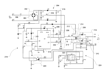
a stable direct
current (DC) voltage. Such circuitry typically includes a rectifier, or
equivalent circuitry, and
a DC-DC converter circuit, or equivalent circuitry. The rectifier receives the
AC input and
provides an unregulated DC output. The DC-DC converter circuit receives the
unregulated
DC output from the rectifier and provides a stable, regulated DC output to the
solid state light
source.
[0004] A variety of DC-DC converter circuit configurations are well-known in
the art.
Certain types of known DC-DC converter circuit configurations, such as but not
limited to
buck converters, boost converters, buck-boost converters, etc., are generally
categorized as
switching regulators. These devices include a switch, e.g. a transistor, which
is selectively
operated to allow energy to be stored in an energy storage device, e.g. an
inductor, and then
transferred to one or more filter capacitors. The one or more filter
capacitors provide a
relatively smooth DC output voltage to the load (i.e., the solid state light
source) and provide
essentially continuous energy to the load between energy storage cycles.
Page 1 of 19
CA 02841966 2014-01-13
WO 2013/012529
PCT/US2012/044479
SUMMARY
[0005] Conventional switching regulator configurations typically have no
protective isolation
between the unregulated DC voltage and the regulated DC output voltage. In
some
configurations, the unregulated DC voltage may be 400 Volts or more. The
unregulated DC
voltage may be dangerous (i.e., cause damage or destruction) if inadvertently
applied to the
load. Further, conventional switching regulator configurations typically
involve a pulsed
current draw from the AC power source in a manner that results in a less than
optimum
power factor. The power factor of a system is defined as the ratio of the real
power flowing
to the load to the apparent power, and is a number between 0 and 1 (or is
expressed as a
percentage, e.g. 0.5 pf = 50% pf). The real power is the actual power drawn by
the load. The
apparent power is the product of the current and voltage applied to the load.
For systems
with purely resistive loads, the voltage and current waveforms are in phase,
changing polarity
at the same instant in each cycle. Such systems have a power factor of 1.0,
which is
commonly referred to as "unity power factor." Where reactive loads are
present, such as with
loads including capacitors, inductors, or transformers, energy storage in the
load results in a
time difference between the current and voltage waveforms. This stored energy
returns to the
source and is not available to do work at the load. Systems with reactive
loads often have
less than a unity power factor. A circuit with a low power factor will use
higher currents to
transfer a given quantity of real power than a circuit with a high power
factor.
[0006] Further, in typical solid state light source driver circuits, there is
a design tradeoff
between output ripple current versus capacitance. A high output ripple current
may result in
a noticeable flicker in the load (i.e., solid state light source or sources),
an undesirable
outcome particularly for lighting apparatus intended for constant
illumination. This ripple
current may be reduced by increasing output bulk capacitance. However,
increasing the
output bulk capacitance results in decreased power efficiency as well as
greater cost, both of
which are also undesirable.
[0007] Generally, embodiments described herein overcome the above described
issues by
providing driver circuitry for a solid state light source based lighting
apparatus, where the
driver circuitry provides constant current output with low current ripple,
reduced bulk
capacitance, and power factor correction. The lighting apparatus may be a lamp
and/or a
fixture and/or combinations thereof. The solid state light source may be a
single source or a
plurality of sources, and may include one or more light emitting diodes
(LEDs), organic light
emitting diodes (OLEDs), polymer light emitting diodes (PLEDs), and the like,
including
Page 2 of 19
CA 02841966 2016-02-10
various combinations thereof The driver circuitry is configured as a resonate
driver and may
be further configured as a half bridge resonate driver. Power efficiency may
be increased by
controlling the switching frequency of the half bridge inverter through
feedback from an
output stage, and by maintaining zero voltage switching on the inverter
switches.
[0008] In an embodiment, there is provided a driver circuit comprising: a
rectifier circuit
configured to receive an AC input voltage and provide an unregulated DC
voltage; an inverter
circuit having a first switch and a second switch, the inverter circuit
configured to receive a
first gate control signal and a second gate control signal to open and close
the first switch and
the second switch, respectively, to generate a resonate AC signal from the
unregulated DC
voltage; a transformer comprising: a primary winding coupled to the inverter
circuit; a
secondary winding configured to be coupled, through an output stage circuit,
to a solid state
light source; and a feedback winding wound on a same core with the primary
winding,
configured to provide a fourth signal representative of current through
therein; a power factor
correction circuit configured to control the inverter circuit in response to a
first signal
representative of the unregulated DC voltage and a second signal
representative of current
through the inverter circuit; and a frequency control circuit configured to
generate the first
gate control signal and the second gate control signal to control a switching
frequency of the
inverter circuit in response to a third signal representative of current
though the output stage
circuit and the fourth signal representative of current through the feedback
winding.
[0009] In a related embodiment, the driver circuit may further include a zero
voltage
switching (ZVS) circuit configured to adjust timing of the first gate control
signal and the
second gate control signal, such that the first switch and the second switch
close at a
nominally zero drain to source voltage. In a further related embodiment, the
ZVS circuit may
be further configured to adjust the timing of the first gate control signal
and the second gate
control signal in response to a fifth signal representative of current through
the primary
winding.
[0010] In another related embodiment, the third signal may be optically
coupled from the
output stage circuit to the frequency control circuit. In yet another related
embodiment, the
frequency control circuit may be configured to adjust the switching frequency
of the inverter
circuit to reduce current ripple in the output stage circuit. In still another
related embodiment,
Page 3 of 19
CA 02841966 2016-02-10
current in the output stage circuit may increase in response to a decrease in
the switching
frequency and current in the output stage circuit may decrease in response to
an increase in
the switching frequency.
100111 In another embodiment, there is provided a method of driving a solid
state light
source, comprising: receiving an AC input voltage; converting, within a
rectifier circuit, the
received AC input voltage to an unregulated DC voltage; generating a resonate
AC signal
within an inverter circuit from the unregulated DC voltage, wherein generating
comprises:
receiving a first gate control signal and a second gate control signal; and
opening and closing
a first switch and a second switch of the inverter circuit based on the
received first gate
control signal and the received second gate control signal, respectively;
controlling the
generation of the resonate AC signal within the inverter circuit in response
to a first signal
representative of the unregulated DC voltage and a second signal
representative of current
through the inverter circuit; coupling the resonate AC signal to a primary
winding and a
secondary winding of a transformer, wherein the transformer is connected to
the inverter
circuit; converting the coupled resonate AC signal to a regulated DC output;
and outputting,
via an output stage circuit, the regulated DC output to drive the solid state
light source;
generating the first gate control signal and the second gate control signal,
in a frequency
control circuit, in response to a third signal representative of current
through the output stage
circuit and a fourth signal representative of current through a feedback
winding of the
transformer, so as to control a switching frequency of the inverter circuit,
wherein the
feedback winding and the primary winding are wound on a same core.
[0012] In a related embodiment, the method may further include adjusting
timing of the first
gate control signal and the second gate control signal via a zero voltage
switching (ZVS)
circuit, such that the first switch and the second switch close at a nominally
zero drain to
source voltage. In a further related embodiment, the method may further
include adjusting,
via the ZVS circuit, the timing of the first gate control signal and the
second gate control
signal, in response to a fifth signal representative of current through the
primary winding.
[0013] In another related embodiment, the method may further include:
generating the first
gate control signal and the second gate control signal, in a frequency control
circuit, in
response to a third signal representative of current through the output stage
circuit and a
Page 4 of 19
CA 02841966 2016-02-10
fourth signal representative of current through a feedback winding of the
transformer, so as to
control a switching frequency of the inverter circuit.
[0014] In a further related embodiment, the method may further include
optically coupling the
third signal from the output stage circuit to the frequency control circuit.
In another further
related embodiment, the method may further include adjusting, via the
frequency control
circuit, the switching frequency of the inverter circuit to reduce current
ripple in the output
stage circuit. In still another further related embodiment, the method may
further include
increasing current in the output stage in response to a decrease in the
switching frequency;
and decreasing current in the output stage in response to an increase in the
switching
frequency.
[0015] In another embodiment, there is provided a solid state light source
assembly
comprising: a housing; a solid state light source disposed within the housing;
and a driver
circuit disposed within the housing, the driver circuit comprising: a
rectifier circuit configured
to receive an AC input voltage and provide an unregulated DC voltage; an
inverter circuit
having a first switch and a second switch, the inverter circuit further
configured to receive a
first and a second gate control signal to open and close the first switch and
the second switch,
respectively, to generate a resonate AC signal from the unregulated DC
voltage; a transformer
comprising: a primary winding coupled to the inverter circuit; a secondary
winding
configured to be coupled, through an output stage circuit, to the solid state
light source; and a
feedback winding wound on a same core with the primary winding, configured to
provide a
fourth signal representative of current through therein; a power factor
correction circuit
configured to control the inverter circuit in response to a first signal
representative of the
unregulated DC voltage and a second signal representative of current through
the inverter
circuit; and a frequency control circuit configured to generate the first and
the second gate
control signals to control a switching frequency of the inverter circuit in
response to a third
signal representative of current though the output stage circuit and the
fourth signal
representative of current through the feedback winding.
[00161 In a related embodiment, the driver circuit may further include a zero
voltage
switching (ZVS) circuit configured to adjust timing of the first gate control
signal and the
second gate control signal, such that the first switch and the second switch
close at a
Page 5 of 19
CA 02841966 2016-02-10
nominally zero drain to source voltage. In a further related embodiment, the
ZVS circuit may
be configured to adjust the timing in response to a fifth signal
representative of current
through the primary winding.
[0017] In another related embodiment, the third signal may be optically
coupled from the
output stage circuit to the frequency control circuit. In yet another related
embodiment, the
frequency control circuit may be configured to adjust the switching frequency
of the inverter
circuit to reduce current ripple in the output stage circuit. In still another
related embodiment,
current in the output stage circuit may increase in response to a decrease in
the switching
frequency and current in the output stage circuit may decrease in response to
an increase in
the switching frequency.
BRIEF DESCRIPTION OF THE DRAWINGS
[0018] The foregoing and other objects, features and advantages disclosed
herein will be
apparent from the following description of particular embodiments disclosed
herein, as
illustrated in the accompanying drawings in which like reference characters
refer to the same
parts throughout the different views. The drawings are not necessarily to
scale, emphasis
instead being placed upon illustrating the principles disclosed herein.
Page 5a of 19
CA 02841966 2014-01-13
WO 2013/012529
PCT/US2012/044479
[0019] FIG. 1 is a simplified block diagram of a solid state light source
assembly according
to embodiments disclosed herein.
[0020] FIG. 2 is a block diagram of a resonate driver circuit according to
embodiments
disclosed herein.
[0021] FIG. 3 is a circuit diagram of a resonate driver circuit according to
embodiments
disclosed herein.
[0022] FIGs. 4-6 are block flow diagrams of methods of driving a solid state
light source
according to embodiments disclosed herein.
DETAILED DESCRIPTION
[0023] FIG. 1 shows a block diagram of a solid state light source assembly 100
according to
embodiments described herein. The solid state light source assembly 100
includes a resonate
driver circuit 102 that receives an alternating current (AC) input ACin, and
provides a
regulated direct current (DC) output DCõ,,t to drive a solid state light
source, such as but not
limited to an LED-based light source 104. The LED-based light source 104 may
be, but is
not limited to, a single LED or multiple LEDs interconnected in series and/or
parallel
configurations. In some embodiments, ACir, may be provided directly from a
120VAC/60Hz
line source. Alternatively, or additionally, ACir, may be provided from any
type of AC
source, such as but not limited to a 220-240 VAC at 50-60Hz.
[0024] The resonate driver circuit 102 converts the AC input voltage ACir, to
a regulated DC
output voltage DCõ,,t with a high power factor, high efficiency and low
current ripple. In
some embodiments, the resonate driver circuit 102 and the LED-based light
source 104 are
provided within a single housing to create the solid state light source
assembly 100. The
solid state light source assembly 100, in some embodiments, comprises a lamp.
Alternatively, or additionally, in some embodiments, the solid state light
source assembly 100
comprises a luminaire and/or fixture. A solid state light source assembly 100
including an
LED-based light source 104 provides long life and low power consumption
compared to
those including non-LED-based light sources.
[0025] FIG. 2 is a block diagram of the resonate driver circuit 102. The
driver circuit 102
includes a rectifier 202, a power factor correction circuit 204, an inverter
switch 206, a
transformer 208, and an output stage circuit 216. The transformer 208 includes
including a
primary winding 210, a secondary winding 214, and a feedback winding 212. The
output
stage circuit 216 is coupled to the secondary winding 214 of the transformer
208. The driver
Page 6 of 19
CA 02841966 2014-01-13
WO 2013/012529
PCT/US2012/044479
circuit 102, in some embodiments, includes a zero voltage switching (ZVS)
circuit 222 and a
frequency control circuit 218, which may be optically coupled in a feedback
loop 220 from a
current monitor 224 of the output stage 216.
[0026] The AC input voltage ACir, is coupled to the rectifier circuit 202. The
rectifier circuit
202 is configured to rectify (i.e., convert) ACir, to provide an unregulated
DC output voltage,
i.e. a DC output voltage that follows instantaneous variations in the AC input
voltage. In
some embodiments, the rectifier circuit 202 may include, but is not limited
to, a bridge
rectifier. The rectifier 202, at its output, is coupled to the primary winding
210 of the
transformer 208 through the inverter switch 206 under the control of the power
factor
correction circuit 204, the frequency control circuit 218 and the zero voltage
switching circuit
222. The inverter switch 206, in some embodiments, may be but is not limited
to a half
bridge inverter including a complementary pair of switching transistors. In
general, the
inverter switch 206 converts the unregulated DC output voltage from the
rectifier circuit 202
to a frequency controlled AC voltage coupled to the primary winding 210 of the
transformer
208. Energy stored in the secondary winding 214 is coupled to the output stage
216. The
output stage 216 may, in some embodiments, include a rectifier and a low pass
filter (not
shown in FIG. 2) to convert the AC voltage from the secondary winding 214 to a
DC output
voltage. The low pass filter, in some embodiments, may include a resistor and
capacitor (RC)
network.
[0027] The power factor correction circuit 204 is configured to provide an
output to the
inverter switch 206 so as to control the switch in response to a signal
representative of current
through the inverter switch 206 and a signal representative of the unregulated
DC voltage.
The output from the power factor correction circuit 204 controls the inverter
switch 206 so
that the current to the LED-based light source 104 has a waveform that
substantially matches
and is in phase with the output of the rectifier circuit 202, thereby
providing a high power
factor.
[0028] The ZVS circuit 222 is configured to provide an output to the inverter
switch 206 to
control the switching times of the complementary pair of switching transistors
within the
inverter switch 206 in response to a signal representative of current in the
primary winding
210 of the transformer 208. The ZVS circuit 222 controls the switching times
so that the
complimentary pair of switching transistors close at a time when the drain to
source voltage
of the transistors is substantially zero volts.
[0029] The current monitor circuit 224 is configured to monitor current in the
output stage
circuit 216 associated with the DC output voltage. In embodiments where the
output stage
Page 7 of 19
CA 02841966 2014-01-13
WO 2013/012529
PCT/US2012/044479
circuit 216 includes an RC network, the current monitor 224 monitors current
in the RC
network. The current monitor circuit 224 provides an output through the
optically coupled
feedback path 220 to the frequency control circuit 218. The frequency control
circuit 218 is
configured to provide an output to the inverter switch 206 for controlling the
switch
frequency in response to the optically coupled feedback signal from the
current monitor 224
and a signal representative of current in the feedback winding 212 of the
transformer 208.
The switching frequency may be controlled to adjust the current level and
reduce current
ripple in the output stage 216. In some embodiments, the current level in the
output stage
circuit 216 increases in response to a decrease in the switching frequency and
decreases in
response to an increase in the switching frequency. The signal representative
of current in the
feedback winding 212 may be used to adjust the bias supply of the frequency
control circuit
218 to improve transient response of the frequency control circuit. The
frequency control
circuit 218 may also be configured to prevent both switches in the inverter
switch 206 from
closing at the same time, resulting in a short circuit to ground such as a
crowbar current.
[0030] FIG. 3 is a circuit diagram of the driver circuit 102. The driver
circuit 102 as shown
in FIG. 3 includes a rectifier circuit 202, a power factor correction circuit
204, an inverter
switch 206, a transformer 208 including a primary winding 210, secondary
winding 214 and a
feedback winding 212, and an output stage circuit 216 coupled to the secondary
winding 214
of the transformer 208. The driver circuit 102 may, and in some embodiments
does, include
a zero voltage switching (ZVS) circuit 222 and a frequency control circuit
218, which may be
optically coupled in a feedback loop 220 from a current monitor 224 of the
output stage 216.
[0031] The AC input voltage ACir, is coupled to the rectifier circuit 202. The
rectifier circuit
202 may be configured to rectify ACir, to provide an unregulated DC output
voltage, i.e. a DC
output voltage that follows instantaneous variations in the AC input voltage.
In some
embodiments, for example, the rectifier circuit 202 may include a full bridge
rectifier such as
but not limited to a diode configuration D1 304. An inductor Li 302 may be
employed to
filter line noise on the AC input voltage ACin.
[0032] The output of the rectifier circuit 202 is coupled to the primary
winding 210 of the
transformer 208 through the inverter switch 206, under the control of the
power factor
correction circuit 204, the frequency control circuit 218, and the zero
voltage switching
circuit 222. The inverter switch 206, in some embodiments, may be but is not
limited to a
half bridge inverter including a complementary pair of switching transistors
Q1 306 and Q2
308, as shown in FIG. 3. In general, the inverter switch 206 converts the
unregulated DC
output voltage to a frequency controlled AC voltage coupled to the primary
winding 210 of
Page 8 of 19
CA 02841966 2014-01-13
WO 2013/012529
PCT/US2012/044479
the transformer 208. The energy stored in the secondary winding 214 is coupled
to the output
stage 216. The output stage 216 may, and in some embodiments does, include a
rectifier, D5
and D6, and a low pass filter to convert the AC voltage from the secondary
winding 214 to
the DC output voltage. The low pass filter may, and in some embodiments does,
include a
resistor and capacitor (RC) network 310.
[0033] The power factor correction circuit 204 is configured to provide an
output to the
inverter switch 206 so as to control the switch in response to a signal
representative of current
through the inverter switch 206 and a signal representative of the unregulated
DC voltage.
The output from the power factor correction circuit 204 may control the
inverter switch 206
so that the current to the LED-based light source 104 has a waveform that
substantially
matches and is in phase with the output of the rectifier 202, thereby
providing a high power
factor. The power factor is improved by increasing the current in an inductor
L2 316. When
the switch Q1 306 closes, the current in the inductor L2 316 increases. When
the switch Q1
306 opens, this stored energy in the inductor L2 316 is transferred to a
capacitor C8 318
through the switch Q2 308.
[0034] The ZVS circuit 222 is configured to provide an output to the inverter
switch 206 for
controlling the switching times of the complementary pair of switching
transistors in response
to a signal representative of current in the primary winding 210 of the
transformer 208. The
ZVS circuit 222 may control the switching times so that the switches close at
a time when the
drain to source voltage of the transistors is nominally zero volts. The timing
is determined by
an inductor L3, a capacitor C2, and leakage inductance of the secondary
winding 214 of the
transformer 208.
[0035] The current monitor circuit 224 is configured to monitor current in the
RC network
310 of the output stage circuit 216 associated with the DC output voltage. The
current
monitor circuit 224 may, and in some embodiments does, provide an output
through the
optically coupled feedback path 220 to the frequency control circuit 218. The
current
monitor circuit 224 may, and in some embodiments does, employ an integrated
circuit Ul
320 that regulates the output current as part of a feedback loop between an
internal voltage
reference and an operational amplifier. As the loop gain for the operational
amplifier
increases, the output current ripple decreases. The integrated circuit Ul 320
may be, for
example, but is not limited to an ST Microelectronics TSM 1017 voltage and
current
controller. Those of ordinary skill in the art will recognize, however, that
other known
controllers may be used in place of the TSM 1017 controller shown in FIG. 3.
Page 9 of 19
CA 02841966 2014-01-13
WO 2013/012529 PCT/US2012/044479
[0036] The frequency control circuit is configured to provide an output to the
inverter switch
206 for controlling the switch frequency in response to the optically coupled
feedback signal
from the current monitor 224 and a signal representative of current in the
feedback winding
212 of the transformer 208. The frequency control circuit 218 may, and in some
embodiments does, employ an integrated circuit U2 312 which sets an initial
frequency based
on a resistor network R1, R17 314. After an initialization phase, the
frequency is controlled
by current drain from the RT terminal of the integrated circuit U2 312, which
is tied to the
feedback signal from the optical coupler U5 220. The switching frequency may
be controlled
to adjust the current level and reduce current ripple in the output stage
circuit 216. In some
embodiments, the current level in the output stage circuit 216 increases in
response to a
decrease in the switching frequency and decreases in response to an increase
in the switching
frequency. The integrated circuit U2 312 may be, for example, but is not
limited to a
Fairchild Semiconductor FAN7711 Ballast Control Integrated Circuit. Those of
ordinary
skill in the art will recognize, however, that other known controllers may be
used in place of
the FAN7711 controller shown in FIG. 3. The signal representative of current
in the
feedback winding 212 may be, and in some embodiments is, used to adjust the
bias supply of
the integrated circuit U2 312 of the frequency control circuit 218, through a
diode D8 and a
resistor R2, to improve transient response of the frequency control circuit.
[0037] In some embodiments, the frequency control circuit 218 may also be
configured to
prevent both switches in the inverter switch 206 from closing at the same
time, resulting in a
short circuit to ground known as a crowbar current. This may be accomplished
by
programming the integrated circuit U2 312 to maintain a suitable dead time
between switch
closings for the switches Q1 and Q2.
[0038] A driver circuit according to embodiments described herein may be
configured for
operation with a variety of input voltages based on appropriate selection of
various circuit
components thereof. Table 1 below identifies one example of circuit components
useful in
configuring the embodiment illustrated in FIG. 3 for operation with a 120V
RMs/60Hz AC
input signal (resistor values in ohms):
TABLE 1
Component Descriptor/Value Component Descriptor/Value Component
Descriptor/Value
ACin 120VAC/60Hz L3 166uH R7 lk
C2 72nF Q1 IRF1225 R8 1.5k
C3 luF Q2 IRF1225 R9 820
Page 10 of 19
CA 02841966 2016-02-10
C4 220nF Q3 4N60 R10 1.6
C5 22uF Q4 2SC584500 R12 4.7k
C6 100nF R1 82k R13 1.5k
C7 220nF R2 100 R14 lk
C8 22uF R3 1M R17 47k
C10 100uF R4 68 Ul TSM1017
Li 1.5mH R5 68 U2 FAN7711
L2 360uH R6 10.7k U5 TLP181
[0039] FIGs. 4, 5, 6A, and 6B are flowcharts of various methods 400, 500, 600
of driving a
solid state light source, such as but not limited to an LED-based light
source. The flowcharts
illustrate the functional information one of ordinary skill in the art
requires to fabricate
circuits or to generate computer software to perform the processing required
in accordance
with the present invention. It will be appreciated by those of ordinary skill
in the art that
unless otherwise indicated herein, the particular sequence of steps described
is illustrative
only and may be varied. Thus, unless otherwise stated, the steps described
below are
unordered, meaning that, when possible, the steps may be performed in any
convenient or
desirable order.
[0040] More particularly, FIGs. 4, 5, and 6 show various methods 400, 500, and
600 of
driving a solid state light source. First, an AC input voltage is received,
step 401/501/601.
The received AC input voltage is the converted, within a rectifier circuit, to
an unregulated
DC voltage, step 402/502/602. A resonate AC signal is generated within an
inverter circuit
from the unregulated DC voltage, step 403/503/603. The resonate AC signal is
generated by
receiving a first gate control signal and a second gate control signal, step
404/504/604, and
then opening and closing a first switch and a second switch of the inverter
circuit based on the
received first gate control signal and the received second gate control
signal, respectively, step
405/505/605.
[0041] The generation of the resonate AC signal within the inverter circuit is
controlled in
response to a first signal representative of the unregulated DC voltage and a
second signal
representative of current through the inverter circuit, step 406/506/606. The
resonate AC
Page 11 of 19
CA 02841966 2016-02-10
, .
signal is then coupled to a primary winding and a secondary winding of a
transformer, step
407/507/607, wherein the transformer is connected to the inverter circuit. The
coupled
resonate AC signal is converted to a regulated DC output, step 408/508/608.
Finally, the
Page lla of 19
CA 02841966 2014-01-13
WO 2013/012529
PCT/US2012/044479
Attorney Docket No. 2011P07497W0
regulated DC output is output, via an output stage circuit, to drive the solid
state light source,
step 409/509/609.
[0042] The method 500 shown in FIG. 5 also includes adjusting timing of the
first gate
control signal and the second gate control signal via a zero voltage switching
(ZVS) circuit,
step 510, such that the first switch and the second switch close at a
nominally zero drain to
source voltage. The method 500 further includes adjusting, via the ZVS
circuit, the timing of
the first gate control signal and the second gate control signal, in response
to a fifth signal
representative of current through the primary winding, step 511.
[0043] The method 600 shown in FIGs. 6A and 6B also include generating the
first gate
control signal and the second gate control signal, in a frequency control
circuit, in response to
a third signal representative of current through the output stage circuit and
a fourth signal
representative of current through a feedback winding of the transformer, so as
to control a
switching frequency of the inverter circuit, step 610. The method 600 further
includes
optically coupling the third signal from the output stage circuit to the
frequency control
circuit, step 611, as well as adjusting, via the frequency control circuit,
the switching
frequency of the inverter circuit to reduce current ripple in the output stage
circuit, step 612.
Finally, the method 600 also includes increasing current in the output stage
in response to a
decrease in the switching frequency, step 613, and decreasing current in the
output stage in
response to an increase in the switching frequency, step 614.
[0044] The methods and systems described herein are not limited to a
particular hardware or
software configuration, and may find applicability in many computing or
processing
environments. The methods and systems may be implemented in hardware or
software, or a
combination of hardware and software. The methods and systems may be
implemented in
one or more computer programs, where a computer program may be understood to
include
one or more processor executable instructions. The computer program(s) may
execute on one
or more programmable processors, and may be stored on one or more storage
medium
readable by the processor (including volatile and non-volatile memory and/or
storage
elements), one or more input devices, and/or one or more output devices. The
processor thus
may access one or more input devices to obtain input data, and may access one
or more
output devices to communicate output data. The input and/or output devices may
include one
or more of the following: Random Access Memory (RAM), Redundant Array of
Independent
Disks (RAID), floppy drive, CD, DVD, magnetic disk, internal hard drive,
external hard
drive, memory stick, or other storage device capable of being accessed by a
processor as
Page 12 of 19
CA 02841966 2014-01-13
WO 2013/012529
PCT/US2012/044479
Attorney Docket No. 2011P07497W0
provided herein, where such aforementioned examples are not exhaustive, and
are for
illustration and not limitation.
[0045] The computer program(s) may be implemented using one or more high level
procedural or object-oriented programming languages to communicate with a
computer
system; however, the program(s) may be implemented in assembly or machine
language, if
desired. The language may be compiled or interpreted.
[0046] As provided herein, the processor(s) may thus be embedded in one or
more devices
that may be operated independently or together in a networked environment,
where the
network may include, for example, a Local Area Network (LAN), wide area
network (WAN),
and/or may include an intranet and/or the internet and/or another network. The
network(s)
may be wired or wireless or a combination thereof and may use one or more
communications
protocols to facilitate communications between the different processors. The
processors may
be configured for distributed processing and may utilize, in some embodiments,
a client-
server model as needed. Accordingly, the methods and systems may utilize
multiple
processors and/or processor devices, and the processor instructions may be
divided amongst
such single- or multiple-processor/devices.
[0047] The device(s) or computer systems that integrate with the processor(s)
may include,
for example, a personal computer(s), workstation(s) (e.g., Sun, HP), personal
digital
assistant(s) (PDA(s)), handheld device(s) such as cellular telephone(s) or
smart cellphone(s),
laptop(s), handheld computer(s), or another device(s) capable of being
integrated with a
processor(s) that may operate as provided herein. Accordingly, the devices
provided herein
are not exhaustive and are provided for illustration and not limitation.
[0048] References to "a microprocessor" and "a processor", or "the
microprocessor" and "the
processor," may be understood to include one or more microprocessors that may
communicate in a stand-alone and/or a distributed environment(s), and may thus
be
configured to communicate via wired or wireless communications with other
processors,
where such one or more processor may be configured to operate on one or more
processor-
controlled devices that may be similar or different devices. Use of such
"microprocessor" or
"processor" terminology may thus also be understood to include a central
processing unit, an
arithmetic logic unit, an application-specific integrated circuit (IC), and/or
a task engine, with
such examples provided for illustration and not limitation.
[0049] Furthermore, references to memory, unless otherwise specified, may
include one or
more processor-readable and accessible memory elements and/or components that
may be
internal to the processor-controlled device, external to the processor-
controlled device, and/or
Page 13 of 19
CA 02841966 2014-01-13
WO 2013/012529
PCT/US2012/044479
Attorney Docket No. 2011P07497W0
may be accessed via a wired or wireless network using a variety of
communications
protocols, and unless otherwise specified, may be arranged to include a
combination of
external and internal memory devices, where such memory may be contiguous
and/or
partitioned based on the application. Accordingly, references to a database
may be
understood to include one or more memory associations, where such references
may include
commercially available database products (e.g., SQL, Informix, Oracle) and
also proprietary
databases, and may also include other structures for associating memory such
as links,
queues, graphs, trees, with such structures provided for illustration and not
limitation.
[0050] References to a network, unless provided otherwise, may include one or
more
intranets and/or the internet. References herein to microprocessor
instructions or
microprocessor-executable instructions, in accordance with the above, may be
understood to
include programmable hardware.
[0051] Unless otherwise stated, use of the word "substantially" may be
construed to include a
precise relationship, condition, arrangement, orientation, and/or other
characteristic, and
deviations thereof as understood by one of ordinary skill in the art, to the
extent that such
deviations do not materially affect the disclosed methods and systems.
[0052] Throughout the entirety of the present disclosure, use of the articles
"a" and/or "an"
and/or "the" to modify a noun may be understood to be used for convenience and
to include
one, or more than one, of the modified noun, unless otherwise specifically
stated. The terms
"comprising", "including" and "having" are intended to be inclusive and mean
that there may
be additional elements other than the listed elements.
[0053] Elements, components, modules, and/or parts thereof that are described
and/or
otherwise portrayed through the figures to communicate with, be associated
with, and/or be
based on, something else, may be understood to so communicate, be associated
with, and or
be based on in a direct and/or indirect manner, unless otherwise stipulated
herein.
[0054] Although the methods and systems have been described relative to a
specific
embodiment thereof, they are not so limited. Obviously many modifications and
variations
may become apparent in light of the above teachings. Many additional changes
in the details,
materials, and arrangement of parts, herein described and illustrated, may be
made by those
skilled in the art.
Page 14 of 19