Note: Descriptions are shown in the official language in which they were submitted.
CA 02842057 2017-02-06
TITLE: STREAMLINED APPARATUS AND METHODS FOR RFID COMMUNICATION
[00011
FIELD
100021 The embodiments described herein relate to apparatuses and
methods for
detecting radio-frequency identification (RFD) signals and in particular to
apparatuses
and methods for detecting RFID signals using an integrated circuit RFID
reader,
INTRODUCTION
[0003] RFID is a contactless communication technology that uses
electromagnetic waves to exchange data between a pair of devices colloquially
known
as an RFID tag and an RFID reader, for the purposes of automatic
identification or
tracking of people, animals, products or other objects.
16 (00041 An RFID tag, sometimes also called an RFID label or proximity
integrated
circuit card (PICC), generally comprises an integrated circuit (IC) end an
antenna. Other
elements, such as a processor, may also be included or integrated with the IC.
The
integrated circuit can be used to store and process information, modulate and
demodulate a radio-frequency (RF) signal and perform other functions. The
antenna is
used for transmitting and receiving the RF signal.
[0005) Tags may be generally classified as passive or active. Passive
tags can be
powered via an external electromagnetic field, such as that supplied by the
RFD reader.
Active tags may use a battery to power the integrated circuit and other
elements. In
some cases, a battery may be used to assist in transmission to provide greater
range, or
to power other elements associated with the tag device,
[0006) An RFID reader, sometimes also called an RFID interrogator or
proximity
coupling device (POD), generally comprises an antenna, an RF transmitter for
transmitting a carrier signal, an antenna for coupling the carrier signal with
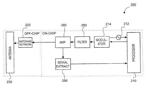
an RFID tag,
an RF receiver for detecting the coupled carrier signal and a decoder for
extracting the
signal information encoded by the RHO tag from the coupled carrier signal.
Typically,
the same antenna is used both to transmit the carrier signal and detect the
coupled
signal from the RFID tag. The RFID reader may also modulate the carrier signal
to
- 1 -
CA 02842057 2014-01-09
WO 2013/006954
PCT/CA2012/000659
transmit information to the RFID tag. In some cases, the RFID reader may also
comprise other elements, such as a microprocessor, to enable more advanced
processing or communication.
[0007] One widely-used standard for RFID applications is the ISO/IEC
14443
standard, the entire content of which is hereby incorporated by reference. The
standard
describes different modulation methods, coding schemes and protocol
initialization
procedures, depending on the type of tag (e.g., Type A or Type B). Other
related
standards for RFID applications, such as MIFARE and FeliCA, are also in use or
development.
[0008] In the ISO/IEC 14443 system, tags may have a proximity operating
range
of less than 10 cm. In the case of credit card-based RFID systems, the
operation range
may be less than 1 cm. According to ISO/IEC 14443, Type A and Type B RFID tags
may not have an active power source and may be powered by the RFID reader via
inductive coupling. The RFID reader transmits a 13.56 MHz carrier signal,
which is used
to power the tags, and which is also modulated by both the reader and card to
exchange
information.
SUMMARY
[0009] In a first broad aspect, there is provided an integrated
circuit frontend for
use in RFID communication, wherein a data signal is transmitted via load
modulation of
a primary signal transmitted via an antenna, the frontend comprising: a signal
generation unit for generating the primary signal; an integrated filter for
reducing
undesired harmonics in the primary signal; an amplifier for amplifying the
filtered primary
signal for transmission via the antenna; a sensor; and a signal extraction
unit configured
to extract the data signal based on variations in a current level or voltage
level detected
by the sensor, wherein the variations in the current level or voltage level
correspond to
the load modulation.
[0010] In some embodiments, the sensor detects the current level
supplied by the
amplifier. In other embodiments, the sensor detects the current level drawn by
the signal
generation unit.
[0011] In some cases, the signal generation unit comprises a modulator, a
clock
signal generator coupled to the modulator, and a processor coupled to the
modulator
and the clock signal generator.
- 2 -
CA 02842057 2014-01-09
WO 2013/006954
PCT/CA2012/000659
[0012] In some cases, the integrated filter is a low pass filter. In
some cases, the
amplifier is a class D amplifier.
[0013] In another broad aspect, there is provided an RFID
communication unit for
detection of a data signal transmitted by a target device via load modulation
of a primary
signal, the RFID communication unit comprising: a signal generation unit for
generating
the primary signal; an integrated filter for reducing undesired harmonics in
the primary
signal; an amplifier for amplifying the filtered primary signal, a sensor; an
antenna for
electromagnetically coupling output from the amplifier with the target device,
such that
the load modulation causes variations in a current level or voltage level
detected by the
sensor via electromagnetic coupling; a signal extraction unit configured to
extract the
data signal based on the variations in the current level or voltage level
detected by the
sensor.
[0014] In some embodiments, the sensor detects the current level
supplied by the
amplifier. In other embodiments, the sensor detects the current level drawn by
the signal
generation unit.
[0015] In some cases, the signal generation unit comprises a
modulator, a clock
signal generator coupled to the modulator, and a processor coupled to the
modulator
and the clock signal generator.
[0016] In some cases, the integrated filter is a low pass filter. In
some cases, the
amplifier is a class D amplifier.
[0017] In some embodiments, the signal generation unit, the integrated
filter, the
amplifier, the sensor and the signal extraction unit are provided on an
integrated circuit.
[0018] In some embodiments, the RFID communication unit further
comprises a
matching network coupled to an input of the antenna.
[0019] In some embodiments, the antenna is formed by a speaker coil.
[0020] In a further broad aspect, there is provided an RFID
communication unit
for detection of a data signal transmitted by a target device via load
modulation of a
primary signal, the RFID communication unit comprising: a signal generation
unit for
generating the primary signal; an integrated filter for reducing undesired
harmonics in
the primary signal; a signal extraction unit; a sensor; and a speaker
comprising: an
amplifier for amplifying the filtered primary signal; and a speaker coil for
- 3 -
CA 02842057 2014-01-09
WO 2013/006954
PCT/CA2012/000659
electromagnetically coupling the primary signal with the target device, such
that the load
modulation causes variations in the primary signal via electromagnetic
coupling; wherein
the sensor is configured to detect a current level or voltage level supplied
by the
amplifier, and wherein the signal extraction unit is configured to extract the
data signal
based on the variations in the current level or voltage level detected by the
sensor.
DRAWINGS
[0021] For
a better understanding of the various embodiments described herein,
and to show more clearly how they may be carried into effect, reference will
now be
made, by way of example only, to the accompanying drawings which show at least
one
exemplary embodiment, and in which:
FIG. 1 is a simplified circuit diagram of an example prior art RFID reader;
and
FIG. 2 is a simplified circuit diagram of an example RFID reader in
accordance with some embodiments.
[0022] The skilled person in the art will understand that the drawings,
described
below, are for illustration purposes only. The drawings are not intended to
limit the
scope of the applicants' teachings in any way.
DESCRIPTION OF VARIOUS EMBODIMENTS
[0023] It
will be appreciated that for simplicity and clarity of illustration, where
considered appropriate, reference numerals may be repeated among the figures
to
indicate corresponding or analogous elements or steps. In addition, numerous
specific
details are set forth in order to provide a thorough understanding of the
exemplary
embodiments described herein. However, it will be understood by those of
ordinary skill
in the art that the embodiments described herein may be practiced without
these
specific details. In other instances, well-known methods, procedures and
components
have not been described in detail since these are known to those skilled in
the art.
Furthermore, it should be noted that this description is not intended to limit
the scope of
the embodiments described herein, but rather is presented for the purposes of
describing one or more exemplary implementations.
[0024] Conventional RFID reader devices are commonly implemented using an
integrated circuit and an external circuit for interfacing with an external
antenna. The
RFID reader integrated circuit has one or more transmit (TX) outputs, or pins,
usable to
- 4 -
CA 02842057 2014-01-09
WO 2013/006954
PCT/CA2012/000659
transmit a primary signal (e.g., a carrier signal or interrogation signal) to
an RFID tag,
such as a proximity card, via the external circuit and antenna. Further, the
RFID reader
integrated circuit has one or more receive (RX) inputs, or pins, used to
receive the
primary signal from the antenna, where the received signal comprises the
primary signal
and a data signal modulated onto the primary signal by the RFID tag, if any.
[0025]
The data signal can be modulated onto the primary signal via load
modulation by the RFID tag. As the RFID tag and the RFID reader can be
electromagnetically coupled, if the RFID tag is placed within the
electromagnetic field of
the RFID reader's antenna, the RFID tag can draw energy from the
electromagnetic
field. This power consumption can be measured as a voltage drop in the
internal
resistance of the RFID reader antenna. Accordingly, by switching a load
resistance on
or off (to change the amount of energy drawn), the RFID tag can cause a
voltage
change at the RFID reader antenna. The voltage change can be detected at the
RX
input of the RFID reader by measuring the voltage variations of the antenna
when an
RFID tag is modulating the primary signal. Commonly, these voltage variations
are
sensed at the RX input of the RFID reader antenna using envelope detectors,
followed
by filters and comparators for comparing the detected input voltage envelope
with a
reference voltage. Such an approach is described, for example, by Klaus
Finkenzeller,
"RFID Handbook: Fundamentals and Applications in Contactless Smart Cards and
Identification, Second Edition", New York: Wiley & Sons Ltd, 2003, the
entirety of which
is incorporated herein by reference.
[0026]
Passive tags in particular may not have sufficient power to produce
relatively strong modulation as compared to the primary signal. Accordingly,
for low
power consumption and high efficiency, RFID tags can transfer data via load
modulation
at a data rate determined in part by a subcarrier frequency. For ISO/IEC 14443
Type A
and Type B systems, the subcarrier frequency is 847.5 kHz, which generally
corresponds to a data rate of 847.5 kbps. In other RFID applications, other
types of
modulation schemes may be employed.
[0027] As
noted above, modulation can be accomplished by switching a load
impedance of the tag on and off. When the tag is within sufficient proximity
of the
reader, and when the reader is activating the tag by transmitting a primary
signal, the
load impedance on the tag may be inductively coupled to the reader antenna.
- 5 -
CA 02842057 2014-01-09
WO 2013/006954
PCT/CA2012/000659
Accordingly, the amplitude of the primary signal on the reader antenna will be
modulated in response to the switching load impedance of the tag.
[0028] A
conventional transmitter portion of an RFID reader is well-understood
and relatively straightforward to design with given specifications. For
example, in order
to reduce the electromagnetic noise radiated via the antenna, the external
circuit
commonly has an electromagnetic compatibility (EMC) filter for filtering the
data signal
to be transmitted. A typical EMC filter comprises an inductor and a capacitor
forming a
low-pass filter (LPF).
[0029]
However, the use of an EMC filter and other off-chip components in the
antenna interface imposes design constraints on the RFID reader. Accordingly,
there is
provided herein an architecture that combines amplifiers, on-chip filters,
current sensors
and digital post processing to generate a transmitted signal or to recover
information
from a transmitted signal (e.g., which uses Amplitude Shift-Keying (ASK)
modulation)
that eliminates the need for EMC filters at the antenna TX pin, and further
eliminates the
need for a separate antenna RX input.
[0030]
Accordingly, the architecture described herein provides a novel 13.56 MHz
RFID analog frontend design that is suitable for contactless card and
contactless reader
applications such as ISO/IEC 14443 Type A or Type B.
[0031]
Referring now to FIG. 1, there is shown a simplified circuit diagram of an
example prior art RFID reader. RFID reader 100 demonstrates an analog frontend
design targeted for ISO/IEC 14443 applications. Under this approach, the
receiver of
RFID reader 100 employs an envelope detector to extract the envelope of the
carrier for
subsequent filtering and amplification, before conversion to a digital signal.
RFID reader
100 may comprise a processor 110, clock signal generator 112, modulator 114,
EMC
filter 122, matching networks 124 and 125, antenna 130, envelope detector 140,
amplifier 150, filter 160 and comparator 170.
[0032]
Processor 110 may be a digital signal processor, field programmable gate
array or general purpose processor used to generate signals for encoding and
transmitting to an RFID tag, and for decoding signals received from an RFID
tag.
[0033] The transmitter portion of RFID reader 100 may comprise the
processor
110, clock signal generator 112, modulator 114 and the antenna network
comprising
EMC filter 122, matching networks 124 and 125 and antenna 130. A digital input
signal
- 6 -
CA 02842057 2014-01-09
WO 2013/006954
PCT/CA2012/000659
from processor 110, is input to modulator 114 for modulation. Modulator 114
may be an
ASK modulator. A clock signal generator 112 may provide a reference signal to
be
modulated by modulator 114 using the input signal provided by processor 110.
For
example, for an ISO/IEC 14443 application, the reference signal may be a
periodic
signal with a frequency of 13.56 MHz (e.g., carrier frequency). The reference
signal may
be filtered to generate a sinusoidal primary signal.
[0034]
Processor 110, clock signal generator 112 and modulator 114 may be
collectively referred to as a signal generation unit.
[0035]
Following modulation, the modulated primary signal may pass through an
electromagnetic compatibility (EMC) filter 122 and an antenna impedance
matching
network 125. Subsequently, the modulated primary signal may be transmitted by
antenna 130. Typically, the EMC filter, matching network and the antenna are
implemented off-chip.
[0036]
The receive portion of RFID reader 100 detects information from the RFID
tag, which may be transmitted by load modulation at the tag and inductively
coupled to
the same antenna 130.
[0037] A
rectifier-based envelope detector 140 may be used to extract the carrier
envelope, which should represent the baseband signal. In practice, a rectifier-
based
envelope detector suffers greatly from process variations. For example, in a
rectifier-
based envelope detector with an RC network, random process variations can
alter
resistor and capacitor values, resulting in fluctuations in the RC time
constant on the
order of 50%. More advanced designs of rectifier-based envelope detectors
have been
proposed, but the adverse effects of process variation cannot be entirely
eliminated due
to the direct involvement of passive components in envelope tracking.
[0038] Sensitivity and signal to noise ratio (SNR) are generally related
according
to an inverse relationship. This property significantly complicates the design
of a highly
sensitive envelope detector. That is, high sensitivity generally leads to poor
SNR and
high SNR generally leads to low sensitivity.
[0039]
Following envelope detection, the detected envelope may be further
amplified by a variable gain amplifier 150 (VGA) and fed through a bandpass
filter 160
to remove out-of-band noise from the signal. A high quality VGA and bandpass
filter is
- 7 -
CA 02842057 2014-01-09
WO 2013/006954
PCT/CA2012/000659
typically critical in this approach, due to the low SNR of the detected
envelope, as noted
above.
[0040]
Finally, a high gain amplifier or comparator 170 may be used to convert
the output of the bandpass filter 160 to a digital signal. The comparator
threshold is
typically programmable, because this architecture generally cannot fully
remove the DC
component of the baseband signal.
[0041]
Referring now to FIG. 2, there is shown a simplified circuit diagram of an
example RFID reader in accordance with some embodiments. RFID reader 200
demonstrates a frontend design that may be used for ISO/IEC 14443
applications. RFID
reader 200 may comprise a processor 210, clock signal generator 212, modulator
214,
filter 280, amplifier 285, matching network 225, antenna 230 and signal
extraction unit
290.
[0042] In
general, portions of RFID reader 200 may correspond to portions of
RFID reader 100. Accordingly, processor 210, clock signal generator 212,
modulator
214, matching network 225 and antenna 230 may generally correspond to
processor
110, clock signal generator 112, modulator 114, matching network 125 and
antenna
130, respectively.
[0043]
Likewise, processor 210, clock signal generator 212 and modulator 214
may be collectively referred to as a signal generation unit.
[0044] RFID reader 200 demonstrates an analog frontend design targeted for
ISO/IEC 14443 applications. Under this approach, the receiver of RFID reader
200
replaces the conventional receiver portion of RFID reader 100 (e.g.,
comprising RX
antenna voltage detection using envelope detector 140, amplifier 150, bandpass
filter
160 and comparator 170) with signal extraction unit 290, which uses a current
sensing
element to detect current supplied by amplifier 285. Accordingly, the current
sensing
element can detect current variations in a transmitted signal when an RFID tag
is
modulating the electromagnetic field generated by the RFID reader.
[0045] In
alternative embodiments, if desired, the RFID reader can detect the load
modulation by the RFID tag in the conventional manner using an RX input pin as
shown
in RFID reader 100. However, by sensing current at amplifier 285, the
conventional
receiver processing stage can be eliminated. Likewise, the RX pin of the
antenna can be
eliminated or left unused.
- 8 -
CA 02842057 2014-01-09
WO 2013/006954
PCT/CA2012/000659
[0046] If
the RX pin is eliminated, filter 280 can be used to eliminate unwanted
harmonics of the RF field prior to transmission by the antenna. Filter 280 can
be an on-
chip low-pass filter, which may be an active filter or a passive filter. The
frequency
response of filter 280 can be adjusted to compensate for the removal of the
conventional EMC filter (e.g., EMC filter 122), and to provide a desired
transmission
characteristic. Accordingly, the conventional EMC filter (e.g., filter 122)
can be removed.
[0047]
Amplifier 285 can be used to amplify (or buffer) the output of filter 280 and
to provide the primary signal for transmission via antenna 230. In some cases,
amplifier
285 may be a power amplifier or audio amplifier. For example, amplifier 285
may be a
class D audio amplifier.
[0048] A
current sensor can be used to detect current consumed by the RF field
generated by RFID reader 200. In practice, this can be detected, for example,
by
measuring current drawn or supplied by amplifier 285 (e.g., transmission
signal current).
In some cases, current may even be measured elsewhere along the signal
transmission
chain (e.g., at the input of amplifier 285). For ease of exposition, this
current
measurement will be described as a measurement of current supplied by
amplifier 285,
however it will be understood that current could be measured at various other
points in
the signal transmission chain with similar effect.
[0049]
The current sensor may be integrated into amplifier 285, signal extraction
unit 290, or may be a separate element (not shown).
[0050]
The current level can be detected by, or provided to, a signal extraction
unit 290. Signal extraction unit 290 may comprise a suitable filter and signal
processing
logic for post processing the detected current level to generate an extracted
data signal.
As described herein, because an RFID tag that is modulating a primary signal
draws
energy from the electromagnetic field generated by the RFID reader, this load
modulation can be detected in the current supplied by amplifier 285.
[0051] By
eliminating the need for off-chip filters and a RX pin from the antenna, a
variety of alternative antenna configurations can be used. For example, an
audio
speaker comprises a coil, a diaphragm and a magnet. Accordingly, in some
embodiments, the speaker coil may be used as the RFID antenna coil.
Furthermore, as
amplifier 285 can be an audio amplifier, various components of RFID reader 200
may be
integrated with and/or shared with an audio output device. This may facilitate
easy
- 9 -
CA 02842057 2014-01-09
WO 2013/006954
PCT/CA2012/000659
integration of the RFID reader with the audio units of electronic devices such
as cell
phones, personal computers, laptops and tablets.
[0052] It
will be appreciated that for simplicity and clarity of illustration, numerous
specific details of the described embodiments are set forth herein primarily
with
reference to an RFID reader as transmitter and a passive RFID tag as
modulating the
signal transmitted by the RFID reader. However, the described signal detection
approach can also be applied by RFID tags, and active RFID tags in particular.
For
example, an RFID tag may also transmit a signal, and monitor current supplied
by an
output amplifier to detect modulation performed by the RFID reader of the
signal
transmitted by the RFID tag. Likewise, an audio speaker can also be used as an
RFID
tag antenna.
- 10-