Note: Descriptions are shown in the official language in which they were submitted.
CA 02842778 2014-01-22
WO 2013/020213
PCT/CA2012/000736
1
PIEZOELECTRIC SENSORS AND SENSOR ARRAYS FOR
THE MEASUREMENT OF WAVE PARAMETERS IN A FLUID,
AND METHOD OF MANUFACTURING THEREFOR
TECHNICAL FIELD
[0001] The present disclosure generally relates to pressure sensors.
More specifically, but not exclusively, the present disclosure is concerned
with
piezoelectric pressure sensors and with an array of piezoelectric pressure
sensors for wave parameters measurement, and with methods for producing
piezoelectric pressure sensors.
BACKGROUND
[0002] The advance in microfabrication techniques makes it possible
to produce very accurate and versatile sensors used in a variety of systems
involving mechanical, electrical, optical and biological sensing. A major
group
of mechanical sensing devices use the piezoelectric effect to obtain high
speed
detection of a mechanical displacement, a pressure or a force. Because of
their
fast responses, these types of sensors are very popular in applications
involving wave propagation, either shock waves or acoustic waves. Using the
proper sensors and signal conditioning systems, it is possible to provide an
accurate history of pressure variation in a certain location, resulted from
passage of the waves. However, to obtain a complete picture of wave
propagation in the medium it is necessary to probe the medium in different
locations, so that the direction and the speed of the wave could be measured,
in addition to its amplitude time history.
[0003] There are many applications for simple devices that could
measure the local velocity vector of a mechanical wave. Shock tubes have
CA 02842778 2014-01-22
WO 2013/020213
PCT/CA2012/000736
2
been known in the art of fluid mechanics for quite some time. Shock tubes may
be used in the study of unsteady high speed flows. To acquire practical
information on the speed and propagation of a wave in a shock tube, a number
of sensors are typically installed along the length of the shock tube in such
a
manner as to detect change in at least one physical property of a gas
contained in that shock tube.
[0004] Sensing the speed of a wave may, in theory, be made using,
for example, two pressure transducers installed along a shock tube. Measuring
the time taken by the wave to travel between the two transducers and knowing
the distance between them allows for the computation of the average wave
speed over this distance. The wave velocity may have fluctuated when
travelling from one transducer to the next, therefore such a setup allows for
measuring the average speed.
[0005] Furthermore, measuring the direction of propagation of a
wave may, in theory, be made using more than two sensors, wherein this
plurality of sensors is not located on a straight line. However, such a simple
setup may render the measurements inaccurate. This is because the speed
and direction of a pressure wave jointly define a velocity vector whose
properties may depend on the position of the wave. To obtain an accurate
measurement of the local wave velocity vector therefore requires the plurality
of
sensors to be in close proximity. This is difficult to achieve with current
commercial pressure sensors which are packaged individually and which each
occupies a fairly large surface of many square millimeters.
[0006] The same situation may take place in components of
turbomachines, such as fans, compressors and turbines. Many flow
phenomena in gas turbines are unsteady, meaning that the flow properties vary
in time at a certain fixed location, leading to wave propagating in various
CA 02842778 2014-01-22
WO 2013/020213
PCT/CA2012/000736
3
directions. For example, some or all blades within a compressor may stall and
the pressure at a given location may vary in time. To identify the amplitude,
speed and direction of stall waves in such a situation would require the use
of
many pressure sensors in close proximity, a configuration difficult to achieve
in
practice due to the relatively large size of actual pressure sensors and the
limited space available in typical turbomachines.
[0007] Another situation takes place in microdevices where the
space available for measuring the speed of waves is severely limited.
Microscale shock tubes have been introduced for this purpose. Such shock
tubes may have cross sections of the order of a few micrometers. Obviously,
measurements of physical properties of gas taking place in such small scales
cause important difficulties, and the size of sensors cannot exceed the size
of
the channel of the microscale shock tube. Moreover, in operation, these
sensors need to be put in direct contact with the flow of gas and have a
reaction time sufficiently fast to detect gaseous pressure changes occurring
at
nanosecond scales.
[0008] Conventional pressure sensors require the presence of a
mechanical element, such as a membrane, having a shape that may be altered
under pressure in a manner that the shape alteration may be measured.
Miniaturization of the sensors implies a very small and very thin membrane,
difficult to fabricate, whose shape alteration that may only be measured using
technologically complex methods, such as with an atomic force microscope, for
example.
[0009] There therefore exists a need for a method for fabricating
sensors that are simple to operate and yet are sufficiently small that an
array of
them may be packaged in a small area and volume.
CA 02842778 2014-01-22
WO 2013/020213
PCT/CA2012/000736
4
SUMMARY
[0010] According to the present disclosure, there is provided a
method for manufacturing a piezoelectric sensor. An electrical barrier is
formed
on top of a silicon substrate. A bottom electrode layer defining a bottom
positive electrode section and a bottom negative electrode section is
deposited
on top of the electrical barrier. A piezoelectric layer is deposited on top of
the
bottom electrode layer. A positive electrode connection area and a negative
electrode connection area are etched, through the piezoelectric layer. A top
electrode layer is deposited on top of the piezoelectric layer. The top
electrode
layer is making contact with the bottom electrode layer through the positive
and
negative electrode connection areas and defines a upper positive electrode
section and a upper negative electrode section. A sensing area is created, in
the piezoelectric layer, in an area of overlap between the upper positive
electrode section and the bottom negative electrode section or between the
upper negative electrode section and the bottom positive electrode section.
[0011] According to the present disclosure, there is also provided
a piezoelectric sensor comprising a silicon substrate, an electrical barrier
on
top of the silicon substrate, a bottom electrode layer on top of the
electrical
barrier, a piezoelectric layer on top of the bottom electrode layer, and a top
electrode layer on top of the piezoelectric layer. The bottom electrode layer
defines a bottom positive electrode section and a bottom negative electrode
section. The piezoelectric layer defines a positive electrode connection area
and a negative electrode connection area. The top electrode layer makes
contact with the bottom electrode layer through the positive and negative
electrode connection areas and defines a upper positive electrode section and
a upper negative electrode section. A sensing area is defined, in the
piezoelectric layer, in an area of overlap between the upper positive
electrode
section and the bottom negative electrode section or between the upper
negative electrode section and the bottom positive electrode section.
CA 02842778 2014-01-22
WO 2013/020213
PCT/CA2012/000736
[0012] According
to the present disclosure, there is also provided
a method of measuring an amplitude, a speed and a direction of propagation of
a shock wave in a shock tube. A piezoelectric sensor array comprising a
plurality of piezoelectric sensors disposed in a pre-defined configuration is
attached to the shock tube. The piezoelectric sensor array is connected to a
signal analysis device. The shock wave is initiated in the shock tube. The
signal analysis device detects an arrival time of the shock wave at each of
the
plurality of piezoelectric sensors.
[0013] The present
disclosure further relates to a smart pressure
sensor array comprising a plurality of sensors packaged in close proximity in
the sensor array, and one or more wired connections for connecting the
sensors to a data acquisition system. The sensor array provides the data
acquisition system with pressure time histories at an individual location of
each
sensor of the array.
BRIEF DESCRIPTION OF THE DRAWINGS
[0014] In the appended drawings:
[0015] Figure 1 is
a schematic diagram illustrating the operational
difference between a single conventional pressure sensor and a smart array of
pressure sensors;
[0016] Figure 2 is
a top plan, schematic view of an example of
circular sensor array comprising eight (8) sensors;
[0017] Figure 3 is
a graph representing measured times versus an
angle of each sensor of the circular sensor array of Figure 2;
CA 02842778 2014-01-22
WO 2013/020213
PCT/CA2012/000736
6
[0018] Figure 4 is a top plan, schematic view of an example of
cross-shaped sensor array comprising five (5) sensors;
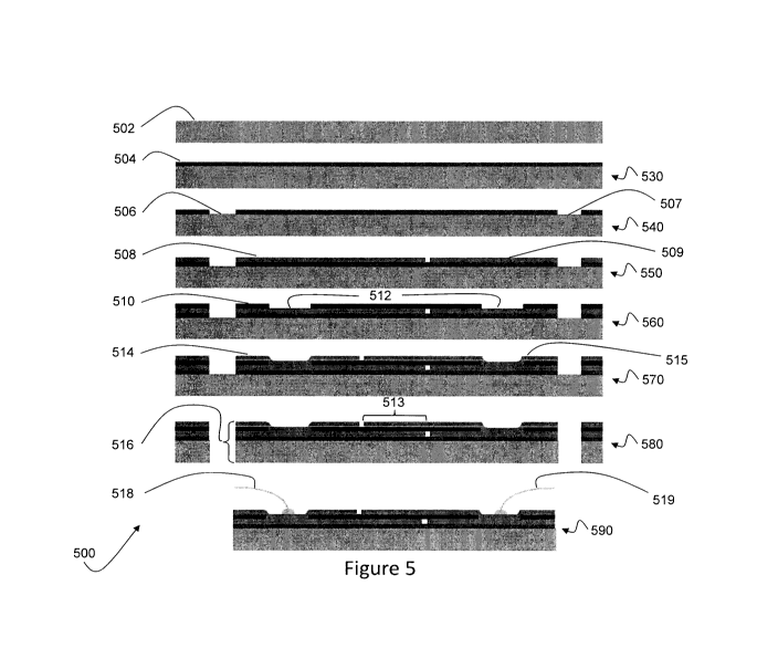
[0019] Figure 5 is a sequence of cross-sectional elevation views
showing examples of operations that may be used in the production of a
sensor;
[0020] Figure 6 illustrates a top plan view and a cross sectional
elevation view of a piezoelectric pressure sensor, produced using the method
of Figure 5;
[0021] Figure 7 is a top plan view of a ring sensor array comprising
eight (8) sensors;
[0022] Figure 8 is a perspective view of an example of packaging for
supporting the ring-shaped array of eight (8) piezoelectric sensors of Figure
7;
[0023] Figure 9 is a sequence of cross-sectional elevation views
showing alternate examples of operations that may be used in the production
of the sensor array for advanced packaging;
[0024] Figure 10 is a close-up, cross-sectional elevation view of the
sensor array produced using the operations of Figure 9;
[0025] Figure 11 is an example of a packaging method for the
sensors arrays fabricated using the process shown in Figure 9;
CA 02842778 2014-01-22
WO 2013/020213
PCT/CA2012/000736
7
[0026] Figure 12 is a flow chart of examples of operations of a
method of simultaneously measuring an amplitude time history, a speed and a
direction of propagation of a shock wave or mechanical wave in flow; and
[0027] Figure 13 is an elevation view of an example of set up for
measuring the speed and direction of propagation of a wave.
DETAILED DESCRIPTION
[0028] The foregoing and other objects, advantages and features of
the present disclosure will become more apparent upon reading of the following
non-restrictive description of illustrative embodiments thereof, given by way
of
example only with reference to the accompanying drawings.
[0029] Generally stated, sensors and sensor arrays described herein
may be applied to measuring a physical property of a fluid such as a gas or
liquid, for example pressure of the gas in a shock tube. Many pressure sensors
may be fabricated and packaged into a device comprising an array of sensors
occupying no more space than a single conventional pressure sensor. A
possible application of the arrays of theses sensors with particular
geometries
comprises measuring the amplitude, speed and the direction of propagation of
waves in a fluid. Simultaneous local measurement of wave amplitude, speed
and direction with great spatial and temporal resolutions may be obtained with
high accuracy. Another possible application is the measurement of wave speed
and wave propagation direction in turbomachinery such as fans, compressors
and turbines. A non-limitative example of implementation is an array of
sensors
comprising five (5) to eight (8) sensors, the sensors being positioned in a
pre-
defined configuration or geometry, for example a circular geometry or a cross-
shaped configuration.
CA 02842778 2014-01-22
WO 2013/020213
PCT/CA2012/000736
8
[0030] Piezoelectric direct sensing pressure sensor arrays suitable
for various applications have been fabricated and tested. The sensor arrays
exhibit small size, for each sensor, of the order of a few microns, and fast
time
response, with a natural frequency which may exceed 1 GHz. Fabrication of
such piezoelectric sensors involves in part processing of piezoelectric
material
such as, for example, Lead Zirconate Titanate (PZT) thin films.
[0031] A circular configuration of the sensor arrays provides a good
resolution in the measurement of the direction of propagation of the wave. A
circular array of eight (8) sensors is sufficient to obtain a small deviation
between theoretical expectations and actual laboratory results. For very high
speed applications, a simpler, cross-shaped array actually requires less post-
processing calculation power.
[0032] While the present disclosure relates mainly to applications of
the sensor array to large scale and microscale shock tubes as well as
turbomachines, those of ordinary skill in the art will appreciate that the
sensor
array may also be used in many other applications where small sensing
devices are used.
[0033] Turning now to drawings, Figure 1 is a schematic diagram
illustrating the operational difference between a single conventional pressure
sensor and a smart array of pressure sensors. The Figure shows the general
idea and compares this smart sensor concept with conventional sensors. For
example, a single conventional pressure sensor 100 measures the pressure
time history at the sensor location, which provides the amplitude of a shock
wave 104 in time but no information about the velocity and the direction of
the
wave propagation.
CA 02842778 2014-01-22
WO 2013/020213
PCT/CA2012/000736
9
[0034] A smart pressure sensor array 102 uses a plurality of sensors
S, packaged in the same device 102 in close proximity to provide the pressure
time histories at each individual sensor location. By simultaneously analyzing
the pressure time histories at different positions it is possible to very
accurately
calculate the speed and also the direction of propagation of the wave 104. The
sensors S, may be wired individually to a data acquisition and analysis system
106 or the signals from different sensors S, of the array 102 may be coded at
an encoder 108 and merged into one signal that may be transmitted with a
single wire 110 and then separated by a decoder 112 and supplied to the data
acquisition and analysis system 106, as shown in Figure 1.
[0035] Figure 2 is a top plan, schematic view of an example of
circular sensor array comprising eight (8) sensors. Figure 2 illustrates a
circular
array 300 comprising eight (8) sensors S,, which is exposed to the passage of
a
shock wave 302, or mechanical wave. In Figure 2, R is a radius of a circle on
which the sensors S, are located, 0 is an angle between a direction of
propagation 304 of the shock wave 302 and a reference direction 306 on the
circular sensor array 300, and cp, is an angle between the orientation of
every
sensor Sõ relative to a center 308 of the circular sensor array 300 and the
reference direction 306. In an embodiment of the circular sensor array 300, R
=
2800 pm, the eight (8) sensors S, are distributed evenly around a circle of
radius R, yielding an angle of 45 degrees between each pair of adjacent
sensors S, relative to the center 308. At a certain time chosen to be a
measurement time reference (for example the trigger time of oscilloscopes
used for the measurement), the shock wave 302 is at a distance he from the
center 308 and at a distance h, from each sensor S. For this situation, the
distance h, may be calculated using equation (1):
[0036] h, = h, ¨Rcos(cb, ¨0) (1)
CA 02842778 2014-01-22
WO 2013/020213
PCT/CA2012/000736
[0037] Assuming a constant local speed ps of the shock wave 302,
dividing equation (1) by the speed of the shock wave, an arrival time of the
shock wave 302 on each sensor S, may be calculated using equation (2):
R j_
t, = t
s
[0038] u (2)
[0039] In equation (2), t, and t, designate times of arrival of the
shock wave 302 at the center 308 of the circular sensor array 300 and at each
sensor S,, respectively. Equation (2) is of particular interest in that it
relates the
time of arrival t, of the shock wave on each sensor (which is a measurand) and
allows postprocessing calculations for obtaining the speed and the direction
of
propagation of the shock wave.
[0040] Figure 3 is a graph representing measured times of arrival of
the shock wave on each sensor versus an angle of each sensor of the circular
sensor array of Figure 2. An angle a, is defined between a direction of
propagation and an orientation of each sensor Si relative to the center 308 of
the circular sensor array 300. Theoretically, these points are on a cosine
curve
400 having an amplitude R/p, where p is the speed of the shock wave or
mechanical wave, and a phase shift of curve 400 relative to the reference
direction 306 is the angle G. It should be observed that there is some
rotation
of the circular sensor array 300 relative to the shock wave 302 between
Figures 2 and 3; consequently, the value of the angle O differs between these
two Figures.
[0041] Therefore, to find the speed and the direction of propagation
of the shock wave, a cosine curve may be fitted to the data as illustrated in
Figure 3. The proper cosine function may be found using nonlinear least
square method. As shown on Figure 3, experimental data obtained through
CA 02842778 2014-01-22
WO 2013/020213
PCT/CA2012/000736
11
measurement of the circular sensor array 300 of Figure 3 allow for the
accurate
determination of wave speed and direction.
[0042] Some other geometries, for example a cross shape array of 5
sensors, are also possible. Figure 4 is a top plan, schematic view of an
example of cross-shaped sensor array comprising five (5) sensors. The cross-
shaped geometry may make the postprocessing calculation easier and more
accurate. For this geometry we have:
[0043] t2 = tc - (RI ps) sin 0 (3)
[0044] where t, and t2 are the time of arrival of the shock wave or
mechanical wave to the center of the device and the outer sensor S2)
respectively. Equation 3 again relates the arrival time of the shock wave on
each sensor (which is a measurand) to the speed and the direction of the
shock wave. Doing the same calculation for all the outer sensors S1, S2, S3
and
S4 we have:
[0045] t, - t1 = (RI ps) cos 6 (4a)
[0046] tc - t2 = (RI ps) sin 0 (4b)
[0047] t, - t3= - (RI ps) cos 0 (4c)
[0048] tc - t4 = - (RI Ps) sin 0 (4d)
[0049] and therefore the wave direction 0 may be obtained from:
CA 02842778 2014-01-22
WO 2013/020213
PCT/CA2012/000736
12
[0050] tan 0 = (t, - t2)/(t, - t1)
= (t, - t4)/(t, - t3)
= (t4 - t,)I(t, - ti)
= (t2 - t,)I(tc t3) (5)
[0051] and the wave speed obtained from:
[0052] Ps = (R cos 0)/(tc - t1)
= (R sin 8)/(t, - t2)
= (R cos 0)/(t3 - tc)
= (R sin 0)/(t4 - tc) (6)
[0053] Since the equations (5) and (6) are over-determined and
there are four (4) different equations for each unknown 0 and Ps, these two
sets
of equations may be used to obtain the final result by averaging over the
computed values or used to eliminate spurious or faulty measurements.
[0054] As a non-limitative example, the circular sensor array 300 of
Figure 2 may take, as illustrated in Figure 7, which is introduced
hereinbelow,
the form of a ring-shaped array 300 of eight (8) sensors S,, equally
distributed
along the ring of the array. One of the sensors Si is delimited by the lines A-
A
and B-B in Figure 7.
[0055] An example of a method of fabrication for the sensor S,
delimited by the lines A-A and B-B of Figure 7, which is introduced
hereinbelow, will now be described with references to Figures 5 and 6.
[0056] Figure 5 is a sequence of cross-sectional elevation views
showing examples of operations that may be used in the production of a
CA 02842778 2014-01-22
WO 2013/020213
PCT/CA2012/000736
13
sensor. In this illustrative embodiment, the sensor Si is a pressure
piezoelectric
sensor. More specifically, the sequence of elevation views of Figure 5 show a
cross section of the sensor Si taken along line C-C of Figure 7, between lines
A-A and B-B.
[0057] The cross-sectional elevation views of Figure 5 schematically
shows operations of a microfabrication procedure 500, wherein each operation
depicts addition or removal of layered components on a 380 micron thick
silicon substrate 502. As a non-limitative example, the silicon substrate 502
is a
single side polished (SSP) substrate, with a [100] Miller index crystal
orientation.
[0058] A first operation 530 comprises a thermal oxidation of the
polished face of the substrate 502. This operation 530 produces an
approximately 600 nanometers (nm) thick oxide layer 504 acting as an
electrical barrier on top of which other layers will subsequently be added.
[0059] At operation 540, the oxide layer is etched away, using any
suitable etching process known to those of ordinary skill in the art, for
example
Inductively Coupled Plasma (ICP) etching with CF4 chemistry, in regions 506
and 507 (corresponding to lines A-A and B-B of Figure 7, respectively). This
will allow to perform the process of Deep Reactive Ion Etching (DRIE) to cut
the chips with the desired shape out of the silicon substrate 502, at the end
of
the microfabrication procedure 500.
[0060] A bottom electrode layer comprising a bottom ground
electrode section 508 and a bottom live electrode section 509 of the sensor Si
is produced in operation 550 by depositing a 15 nm thick sub-layer of titanium
forming an adhesion layer on the oxide layer 504 and, then, a 150 nm thick
sub-layer of platinum as bottom electrodes. Both platinum and titanium sub-
CA 02842778 2014-01-22
WO 2013/020213
PCT/CA2012/000736
14
layers may be deposited in an electron beam evaporator or a sputtering
chamber and annealed at 5700C in nitrogen ambient. As can be seen in Figure
6, the bottom live electrode section 509 is etched, using any suitable etching
process known to those of ordinary skill in the art, in the bottom electrode
layer
(see area 509'), the rest of the bottom electrode layer forming the bottom
ground electrode section 508. The bottom electrode layer may also be etched
at locations 506 and 507, in preparation for operation 580, which is described
hereinbelow. An example of bottom platinum electrode patterning process is
the use of Lift Off Resist (LOR) as sacrificial layer underneath platinum in
etching area, which prevent the platinum from adhering to the surface.
[0061] At operation 560, a piezoelectric layer 510, for example a
PZT layer, having for example a 50 to 500 nm thickness, is deposited by the
sol-gel method on the bottom electrode sections 508 and 509. The sol-gel
method is a wet-chemical technique starting from a chemical solution (or sol)
which acts as a precursor for an integrated network (or gel) of either
discrete
particles or network polymers, as described in more detail at
http://en.wikipedia.orq/wiki/Sol-qel. The operation 560 may include a number
of
cyclic depositions, pyrolyzing and annealing operations to obtain a desired
thickness of the piezoelectric layer 510. In this manner, for example, a good
quality sol-gel derived Lead Zirconate Titanate (PZT) layer can be developed,
free of cracks, by overcoming problems such as diffusion and oxidation of
titanium and residual stresses in the platinum sub-layer. Of course, any other
material capable of producing an electrical field as a result of compression
may
suitably replace PZT.
[0062] The sol-gel derived PZT layer 510 features an extremely
large dielectric constant (in a range of 800-1100), an increased piezoelectric
response and poling efficiency. To electrically connect the bottom electrode
layer to a top electrode layer, which will be added later as described
CA 02842778 2014-01-22
WO 2013/020213
PCT/CA2012/000736
hereinafter, the PZT layer 510 is etched at circular areas 512 (see Figures 5
and 6). The PZT layer may also be etched, using any suitable etching process
known to those of ordinary skill in the art, at locations 506 and 507, in
preparation for operation 580, which is described hereinbelow. An example of
PZT etch process is wet etching in DI:HCI:BOE 206:100:16 solution.
[0063] In a next operation 570, a top electrode layer comprising a
top ground electrode section 514 and a top live electrode section 515 are
produced by depositing a 15 nm thick sub-layer of titanium forming an
adhesion layer on the PZT layer 510 and, then, a 150 nm thick sub-layer of
platinum forming the top electrodes. During operation 570, the top electrode
sections 514 and 515 connect with the bottom electrode sections 508 and 509,
respectively through the etched areas 512 in the PZT layer 510. The same
methods of deposition as employed for the bottom electrode section 508 and
509 may be used. As can be seen in Figure 6, the top live electrode section
515 is etched in the top electrode layer (see combined areas 509' and 515'),
the rest of the top electrode layer forming the top ground electrode section
514.
The top electrode layer may also be etched, using any suitable etching process
known to those of ordinary skill in the art, at locations 506 and 507, in
preparation for operation 580, which is described hereinbelow. As in the case
of bottom platinum electrode patterning, a suitable top platinum electrode
patterning process is the use of Lift Off Resist (LOR) as sacrificial layer
underneath platinum in etching area, which prevent the platinum from adhering
to the surface.
[0064] The overlapping geometry of the bottom electrode layer,
piezoelectric layer and top electrode layer described hereinabove allows to
easily create patterns on the various layers to define a sensor having an
active
area 513 and deactivate the rest of area on the surface of the substrate by
shorting it without removing the piezoelectric material from the deactivated
area
CA 02842778 2014-01-22
WO 2013/020213
PCT/CA2012/000736
16
on the substrate that may cause the delamination of the platinum bottom layer.
Those of ordinary skill in the art will appreciate that operations of Figure 5
may
be used to define one or more sensors. In some embodiments, a plurality of
sensors may be arranged in an array, depending on the created patterns of the
various layers.
[0065] Then, at operation 580, the silicon substrate 502 may be
etched using, for example DRIE, throughout at the regions 506 and 507 to
extract a ring-shape chip comprising eight (8) sensors from the substrate.
Finally, at operation 590, wires such as fine gold wires 518 and 519 are
soldered at areas 512 to respective electrodes formed by electrode sections
508 and 514 and electrode sections 509 and 515.
[0066] Figure 6 illustrates a top plan view and a cross sectional
elevation view of a piezoelectric pressure sensor, produced using the method
of Figure 5. The bottom part of Figure 6 corresponds to the lowest view of
Figure 5; only the wires 518 and 519 are not shown. It may be observed that
the electrode formed by electrode sections 508 and 514 (and wire 518) forms a
ground connection for the sensor while the electrode formed by electrode
sections 509 and 515 (and wire 519) forms a live connection for the sensor,
the
active area 513 of the sensor being between the two connections. In the
example of Figures 5 and 6, the active area 513 comprises a circular area of
the bottom electrode section 508, a circular area of the piezoelectric layer
510
superposed to the circular area of the bottom electrode section 508 and a
circular area of the top electrode section 515 superposed to the circular area
of
the piezoelectric layer 510.
[0067] The foregoing description refers to elements 508 and 514 as
bottom and top 'ground' electrode sections, respectively, and to elements 509
and 515 as bottom and top 'live' electrode sections, respectively. In other
CA 02842778 2014-01-22
WO 2013/020213
PCT/CA2012/000736
17
realizations, elements 508 and 514 may form a live electrode while elements
509 and 515 may form a ground electrode. More generally, any connected pair
of bottom and top electrode sections may act as a positive electrode, the
other
pair of bottom and top electrode sections acting as a negative electrode. It
is
understood that the terms 'positive' and 'negative' reflect relative voltages
between complementary pairs of electrode sections.
[0068] The single ring-shaped array 300 comprising eight (8)
piezoelectric sensors S, of Figure 7 may be fabricated on a four (4) inch
silicon
substrate 502, which may accommodate the simultaneous fabrication of a
plurality of arrays 300 of sensors S,, each fabricated using the method as
described in relation to Figures 5 and 6 followed by etching the substrate
from
the back to extract the ring-shaped sensor arrays.
[0069] In operation, when installed in a sensed device such as a
shock tube, each of the eight (8) piezoelectric pressure sensors reacts to a
shock wave or mechanical wave pressure applied to the PZT layer 510 to
produce an electric signal through the electrode formed by electrode sections
508 and 514 (and wire 518) and the electrode formed by electrode sections
509 and 515 (and wire 519). Electric signals obtained from the sensors may be
amplified and are supplied to a signal analysis device. Signal analysis is
based
on a mathematical model, which may for example be based on Equations (1)
and (2) when the pre-defined configuration of the sensor array is circular as
shown for example in Figures 2 and 7, or based on Equations (5) and (6) when
the pre-defined configuration of the sensor array is a cross as shown for
example in Figure 4.
[0070] Figure 7 is a top plan view of a ring sensor array comprising
eight (8) sensors. A ring-shaped array of eight (8) piezoelectric sensors S,
CA 02842778 2014-01-22
WO 2013/020213
PCT/CA2012/000736
18
should be mounted to a reliable support before it is exposed to wave pressure.
The support also may also be used to establish electrical connections.
[0071] Figure 8 is a perspective view of an example of packaging for
supporting the ring-shaped array of eight (8) piezoelectric sensors of Figure
7.
Packaging 800 of Figure 8 comprises, for example, a number of 0.5 mm tin
plated copper electrical pins 802 extending through a cylindrical ceramic body
804 to form a device capable of being mounted on a printed circuit board (not
shown). The ring-shaped array 300 of Figure 7, which comprises eight (8)
piezoelectric sensors S, fabricated on a silicon substrate 502 etched into an
annular shape, is glued on a flat face of the ceramic body 804, opposite to
the
copper pins 802. Electrical connections (not shown) are established between
the copper pins 802 and the electrodes of the eight (8) piezoelectric sensors
S,
of the ring-shaped array 300 of Figure 7 through fine, for example 50 pm gold
wires such as 806. Eight (8) of the gold wires 806 interconnect the electrodes
of the eight (8) piezoelectric sensors S, formed by electrode sections 509 and
515 with corresponding ones of the copper pins 802. Another one of the gold
wires 806 is used to interconnect a grounding copper pin 802 with the
electrodes of the eight (8) piezoelectric sensors S, formed by the electrode
sections 508 and 514. The electrical connections may be strengthened using
conductive epoxy 808. Finally to obtain a flat surface, any void at the top of
the
ceramic body 804 where the ring-shaped array 300 is located is filled with a
nonconductive epoxy filler 810.
[0072] A challenge in the microfabrication of these sensors is the
elimination of the fine gold wires 518 and 519 from the design of Figure 5
since
topographies on the exposed surface of the sensor may affect the flow over the
sensor.
CA 02842778 2014-01-22
WO 2013/020213
PCT/CA2012/000736
19
[0073] Improving on this design involves wiring out the thin film
piezoelectric structure on the front of substrate to the back side of the
substrate
while keeping the smooth and sealed surface of the sensors. A challenge in the
microfabrication is thus to integrate the sensors' structures with electrical
vias
on a substrate. In fact there are some known approaches to create vias in
silicon substrates. However, these approaches cannot be integrated with the
thin film piezoelectric development procedure described above and a new
approach for the compatible microfabrication of vias is presented.
[0074] Therefore another example of a method of fabrication for the
sensor S, delimited by the lines A-A and B-B of Figure 7 will now be described
with reference to Figure 9, which shows a sequence of cross-sectional
elevation views showing alternate examples of operations that may be used in
the production of the sensor array for advanced packaging. In the description
of
Figure 9, the various materials used as well as the dimensions defining layer
thicknesses are for illustration purposes. Those of ordinary skill in the art
will be
able to adapt those materials and dimensions to the needs of particular
applications.
[0075] Operation 915 starts with production of a Silicon On Insulator
(S01) substrate. The substrate has a 30 pm thick < 100 > silicon device layer
902, 2 pm thick Buried Oxide (BOX) layer 904 forming an upper electrical
barrier, and 300 pm thick lower handle layer 906. These thicknesses are
chosen to meet criteria such as mechanical strength, ease of silicon dry and
wet etch that will be performed later on, enhanced electrical insulation and
less
capacitive parasites.
[0076] At operation 920, to make a reliable mask for the silicon wet
etch, 7 pm thick Plasma Enhanced Chemical Vapor Deposited (PECVD) oxide
layers 908 and 912 are respectively deposited on a front side and on a back
CA 02842778 2014-01-22
WO 2013/020213
PCT/CA2012/000736
side of the substrate. This will allow the substrate to withstand the long 300
pm
silicon wet etch in potassium hydroxyde (KOH) solution.
[0077] At operation 925 the oxide 912 on the lower handle layer 906
is etched 914 using Advanced Oxide Etching (AOE) and an ordinary
photoresist mask to pattern the oxide mask. Proper care in executing this
lithography process will prevent growing of any small flaw during wet etch,
which could make the substrate unusable for the next steps.
[0078] During operation 930 the lower handle layer 906 is etched
through to arrive at the BOX layer 904. The anisotropic etch of silicon in the
KOH solution results in the formation of pits 916 in the lower handle layer
906
with inclined and smooth walls.
[0079] At operation 935, while protecting the BOX layer 904, the
mask oxide layers 908 and 912 are on both sides are wet etched in hydrofluoric
acid bath. To protect the BOX layer 904 in the bottom of the pits 916, the
photoresist is spin coated on the lower handle layer 906 and wiped on the top
surface, followed by plasma burning of the residues of photoresist. This is
repeated for a few times until the bottoms of all the pits 916 are protected.
Then the PECVD masks are removed in, for example hydrofluoric acid or any
other suitable etching solution.
[0080] At operation 940, isolated islands 922 are created on the
device layer 902 by Deep Reactive Ion Etching (DRIE) of annular trenches 924
down to the BOX layer 904. Since the surface of the sensors should not include
any topography, these trenches should be closed with dielectric material.
Therefore, the trenches should be as narrow as possible.
CA 02842778 2014-01-22
WO 2013/020213
PCT/CA2012/000736
21
[0081] At operation 945 the trenches 924 are covered by deposition
of 4 pm thick PECVD oxide 926 on the device layer 902. If the trenches are not
completely covered, the processing materials in the next steps may enter into
the trenches 924 and may short the isolated islands.
[0082] At operation 950, the PECVD oxide 926 is removed from the
surface, using AOE, except at annular areas 928 over the trenches 924. The
PECVD oxide 926 will later be replaced by thermal oxide except over the
trenches 924.
[0083] At operation 955, the entire substrate is thermally oxidized to
1.5 pm oxide thickness after RCA (Radio Company of America) cleaning. This
creates thermal oxide layers 932 and 933 by oxidizing both surfaces of the
substrate as well as inclined walls 934 of the pits 916. This terminal oxide
layer
933 becomes a lower electrical barrier. This process also increases the
thickness of the BOX layer 904 in the pits 916.
[0084] At operation 960, the thermal oxide layer 932 is etched on
isolated islands 936 using AOE to electrically reach to the device layer 902
from the front side of the substrate.
[0085] At operation 965, to electrically reach to the device layer 902
from the back side of the substrate, the BOX layer 904 is etched at annular
areas 938, using AOE. Spray coated photolithography is used to deposit a
uniform layer of photoresist (not shown) on the non-planar surface of the
lower
handle layer 906.
[0086] Bottom electrode sections of the sensors are realized by
deposition of a layer 942 comprising 150 nm of platinum and 15 nm of titanium
CA 02842778 2014-01-22
WO 2013/020213
PCT/CA2012/000736
22
as an adhesion layer, at operation 970. This operation also includes the same
metal deposition on the back side of the substrate, forming layer 944. The
platinum layers 942 and 944 are deposited in an electron beam evaporator and
annealed at 570 C in nitrogen ambient.
[0087] At operation 975, a PZT layer 946 is deposited on the layer
942 by the sol-gel method. To electrically connect the top and bottom
electrode
sections, the PZT film is etched at the desired locations 948.
[0088] At operation 980, top electrode sections 952 are realized by
deposition, on top of the PZT layer 946, of similar layers of platinum and
titanium of the same thicknesses as in operation 970, these layers of platinum
and titanium being etched at desired locations.
[0089] At operation 985, the device layer 902 is deep etched to the
BOX layer 904 at annular area 954 followed by etching of the lower handle
layer 906 to the BOX layer 904 are at annular area 956 to extract circular
chips
from the SOI substrate.
[0090] Figure 10 is a close-up, cross-sectional elevation view of the
sensor array produced using the operations of Figure 9. A chip 1002 as shown
is obtained following operation 985. Within the pits 916, platinum of the
layer
944 fills the annular areas 938 in order to allow connection of the electrodes
with a packaging shown in a later Figure. Trenches 941 etched into the layer
944 ensure isolation between the various connections provided at the various
pits 916 so that, for example, a ground wire may be connected in the pit 916
on
the left hand side of Figure 10 and a live wire may be connected to in the pit
916 on the right hand side of Figure 10. The platinum in the annular areas 938
connects to the bottom and top electrode sections 942 and 952 via the islands
922; the annular trenches 924 ensure isolation between neighboring
CA 02842778 2014-01-22
WO 2013/020213
PCT/CA2012/000736
23
connections within the device layer 902. The bottom electrode layer 942 is
patterned by the etching of trenches 943 in appropriate locations. Likewise,
the
top electrode layer 952 is patterned by the etching of trenches 953 in
appropriate locations. As shown at 947, pattern configurations of the bottom
and top electrode layers 942 and 952 define an active area of the PZT layer
946, sandwiched between overlapping portions of a top electrode section 952
and of a bottom electrode section 942, forming a sensor.
[0091] Figure 11 is an example of a packaging method for the
sensors arrays fabricated using the process shown in Figure 9. In an
embodiment, ease in packaging of the chip 1002 uses a circular chip with a
semicircular notch 1014, for alignment purposes. An easy way to cut the
substrate in this shape is using DRIE.
[0092] The chip 1002 will have a reliable support to be exposed to
the fluid flow and to establish the electrical connections. Referring again to
Figure 11, the packaging comprises a stainless steel casing 1004 and a
machinable ceramic (Macor) support 1006 as the main structure, 0.5 mm
copper wires 1008 are used to establish electrical connections. Electrically
conductive epoxy 1012 is used to attach the wires to the back side of the
chip.
An alignment pin 1010 is used to align the chip with the casing.
[0093] A method for measuring the amplitude, speed and direction
of propagation of a wave in a fluid flow is described below.
[0094] Measuring the speed and propagation direction of a wave in
a fluid flow may be accomplished using a sensor array, for example the ring-
shaped array 300 of eight (8) piezoelectric sensors S, of Figure 7. Figure 12
is
a flow chart of examples of operations of a method of simultaneously
measuring an amplitude time history, a speed and a direction of propagation of
CA 02842778 2014-01-22
WO 2013/020213
PCT/CA2012/000736
24
a shock wave or mechanical wave in flow. A method 1100 is initiated at
operation 1110 after the sensor array has been installed at an appropriate
location within the flow.
[0095] Figure 13 is an elevation view of an example of set up for
measuring the speed and direction of propagation of a wave, for example using
the ring-shaped circular sensor array 300 of Figure 7 in a shock tube. A set
up
1200 comprises a shock tube 1210, and the packaging 800 including the ring-
shaped circular sensor array 300, the ceramic body 804 and the copper pins
802. A relationship of the set up 1200 with the shock wave 302, introduced in
the foregoing description of Figure 3, and its direction 304 of propagation
within
the shock tube 1210 is shown in Figure 13. As the shock wave 302 advances
in the direction 304 along a length of the shock tube 1210, it passes over the
various sensors S, (shown on earlier Figures) of the circular sensor array
300,
at the top of the packaging 800. The shock wave 302 reaches the various
sensors S, in rapid succession.
[0096] Returning to the description of Figure 12, the eight (8)
piezoelectric sensors S, of the ring-shaped array 300 are connected, at
operation 1120, to a signal analysis device (not shown), which may for example
comprise an oscilloscope having a recording mechanism. The flow, in the
present example the shock wave 302, is initiated in the shock tube 1010 at
operation 1130, and reaches the ring-shaped circular sensor array 300 as
described hereinabove. At operation 1140, the signal analysis device detects
an arrival time of each wave, here the shock wave 302, at each of the eight
(8)
piezoelectric sensors Si. Postprocessing of the arrival times on the sensors,
as
processed by the signal analysis device, provides the speed and direction 304
of propagation of the wave, here the shock wave 302, using the formulas (1)
and (2) and the analysis procedure shown in relation to the foregoing
CA 02842778 2014-10-03
description of Figure 3, at operation 1150. Finally, the operations 1140 and
1150 are successively is repeated for each detected wave, in operation 1160.
[0097] Additionally to
their capacity to transform a mechanical signal
into electrical impulses as sensors or receivers, piezoelectric materials can
also
produce mechanical waves if electrically excited appropriately, as emitters.
Accordingly, the sensors arranged and/or fabricated as described in the
present disclosure may also individually be operated as emitters. Individually
tailoring the wave signal simultaneously produced by each emitter in an
emitter
array, operating as a phased array, then allows control over the features of
the
mechanical wave beam produced by the emitter array. Furthermore, the
sensors may successively be used as emitters, to produce for example an
ultrasound beam of short duration, known as a pulse, in the medium into which
they are in contact, and then shortly thereafter as receivers to analyze an
echo
produced by the reflection and refraction of this pulse with various
inhomogeneities in the medium. Operating individual sensors and sensor
arrays in this pulse-echo mode would, for example, allow for the detection of
defects in the medium or imaging the various features in the medium, as it is
already done in ultrasound non-destructive testing (NDT) and imaging. So the
sensors and sensor arrays described here may be used for NDT and imaging,
with new capabilities owing to their small size.
6009906.1