Note: Descriptions are shown in the official language in which they were submitted.
CA 02843546 2014-01-29
WO 2013/017814 PCT/GB2012/000618
Wave Vector Matched Resonator and Bus Waveguide System
Introduction
The present invention relates to an optical device having a low to moderate
refractive
index contrast bus waveguide coupled to one or more nano/microphotonic
resonators
for use in optical communications and in particular for use in wavelength
division
multiplexing (WDM) technology.
Background
Wavelength division multiplexing, referred to as WDM, is a technique utilised
to
increase the transmission capacity of an optical communication system by
allowing
multiple data channels to transit through a single optical transmission line.
Different implementations of the technique have been reported. The most common
approach, illustrated in Figure 1 relies on multiple wavelength lasers
modulated
separately and combined into a single channel by a multiplexer. Fang et al
(Optics
Express, 2008, Vo116, pp 4413) proposed using silicon technology to implement
25
distributed feedback lasers, monolithically coupled to 25 modulators operating
at 40
Gbls and multiplexed together into a single waveguide to form a wavelength
division
multiplexed 1 Tb/s data stream. A problem with this approach is that
interfaces
between the different constituents of the WDM device generate a significant
amount of
back reflection, which destabilises the source(s). Additionally, the
complexity of this
approach results in extremely tight fabrication tolerances, which are
difficult to attain in
practice.
Another approach based on a series of tunable ring resonators with
characteristic
resonant wavelengths attached to a silicon bus waveguide has been demonstrated
by
Dong (Optics express, 2010, Vol18 pp9852) using thermally reconfigurable
microring
resonators and by Xu (Optics Express, 2006, 14, pp9430) using carrier
injection in a
microresonator connected to a PIN junction. This technology allows the
combination of
light filtering, modulation and multiplexing in a single, silicon based
device. However,
the use of a silicon waveguide makes integration of the device with optic
fiber relatively
complex and inefficient due to the mismatch of refractive index between the
two
materials.
Confrimation copy
2
US 6411752 describes a wavelength modulator apparatus that has a series of
vertically
coupled optical ring resonator devices over a cross grid waveguide
architecture. The
resonators arevertically coupled on top of the bus waveguides and are
separated from
the waveguides by a buffer layer. Resonance occurs when light coupled into the
ring
interferes with light passing through the bus waveguide. A problem with the
modulator
described in US 6411752 is that it requires stringent wave vector (defined as
Ik1= 2na,
with the direction perpendicular to the wave fronts) -matching conditions to
be satisfied,
which limit the choices for the materials of the bus waveguide and ring
resonators.
This prevents the use of the most promising configurations for low insertion
loss
operation, such as glass based bus waveguides and silicon ring resonators.
Spot size converters are currently the most popular solution to the general
issue of
coupling between waveguides of different dimension, composition and refractive
index
[see for example US 51990921. This technique requires a tapering of one or
both of the
waveguides in question to achieve a transition between the mismatched modes.
The
fabrication of the taper, in particular, the tip is challenging. While this
approach works
well under ideal conditions [Optics Express 11, 2927-2939 (2003)); in general,
losses of
1.5-2dB per interface are reported. Other problems are that high performance
lithographic techniques are needed to fabricate the converters, and the number
of
devices that can be cascaded is limited due to cumulative losses.
Summary of invention
According to the present invention, there is provided an optical device for
use in optical
communication including: a waveguide of refractive index n, for carrying at
least one
mode at one wavelength, and at least one resonator with a resonant wavelength
that
has a mode volume of less than ten cubic resonant wavelengths, wherein in use
light in
the waveguide is vertically coupled into at least one resonator and the
waveguide and
resonator(s) are adapted, so that wave-vector matching is achieved between at
least
one mode of the resonator and at least one mode of the waveguide.
According to an aspect of the present invention, there is provided a
monolithically
integrated optical device including: a waveguide of refractive index na for
carrying at
least one mode of at least one wavelength, and at least one resonator with a
resonant
wavelength in a layer of material of refractive index nb, wherein the at least
one
CA 2843546 2018-10-18
2a
resonator has a mode volume of less than ten cubic resonant wavelengths,
wherein in
use light in the waveguide is vertically coupled into the at least one
resonator, and the
waveguide and at least one resonator are arranged to provide wave-vector
matching
between at least one mode of the at least one resonator and at least one mode
of the
waveguide, wherein the device further comprises a barrier layer of refractive
index nc,
and a lower cladding layer of refractive index nd, wherein the at least one
resonator is
between the barrier layer and the lower cladding layer, and the waveguide is
on top of
the barrier layer and aligned with the at least one resonator, wherein ne is
less than na;
nc is less than nb; nb is not equal to na, and nd is less than nb.
The resonator(s) may be in a layer of refractive index rib not equal to na,
and the device
further comprises; a barrier layer of refractive index nd, whereby ric< na and
ric< nb, and
a substrate of refractive index nd < nb; wherein the resonator layer is
between the barrier
layer and the substrate, and the waveguide is on top of the barrier layer and
aligned
CA 2843546 2018-10-18
CA 02843546 2014-01-29
WO 2013/017814
PCT/GB2012/000618
3
with the resonator(s), thereby allowing for optical coupling between the
waveguide and
the resonator(s). The lower cladding may have a non-uniform thicknesses and/or
a
non-uniform composition. The barrier layer may have a non-uniform thickness.
The waveguide may be a single mode waveguide or a multimode waveguide.
The resonator(s) carries one or more modes, among which at least one cavity-
mode
overlaps spatially with at least one mode propagating through the waveguide,
thereby
allowing for coupling of light from the waveguide to the resonator.
The device may have N wavelength specific resonators, so as to be operable as
an Nth
order filter.
At least one resonator may be embedded in a PIN junction forming a resonator-
modulator. The at least one resonator-modulator may be an electro-absorption
modulator.
A plurality of the resonators may be coupled together to form a waveguide
acting as an
optical delay line with a "flat-top" spectral response.
The at least one resonator may be adapted to provide two degenerate resonances
at
the resonance frequency.
The waveguide may be a dielectric waveguide or a polymer waveguide. The
waveguide may be made of glass, for example Silicon Oxynitride or TRIPLEX or a
HYDEX.
The resonator may be selected from a wide range of devices, such as a photonic
crystal defect cavity; a plasmonic structure; a nanoantenna or a split ring.
The photonic crystal may be made of Silicon Nitride or of a III-V
semiconductor
material such as Indium Phosphide, Gallium Arsenide, Gallium Nitride or Indium
Gallium Phosphide.
CA 02843546 2014-01-29
WO 2013/017814
PCT/GB2012/000618
4
Where the resonator is a photonic crystal, the resonator may have an
engineered
mode dispersion, so that the optical path inside the resonator is constant
over a given
wavelength interval.
Where the resonator is a photonic crystal, the at least one resonator may be
doped
with material having an absorption band corresponding to the resonant
wavelength of
the doped resonator, wherein a resonant mode coupling into the cavity excites
a
photogenerated carrier.
The resonator may be made of a Silicon/Germanium multilayer.
The optical arrangement may be such that in use light in the waveguide is
coupled
vertically to the at least one resonator.
The device may have multiple resonators, each resonant at a different
wavelength. A
modulator may be associated with each resonator. The modulator may be operable
to
change the resonant wavelength of its associated resonator.
Brief Description of the Drawings
Various aspects of the invention will now be described by way of example only
and with
reference to the accompanying drawings, of which:
Figure 2 shows an exploded perspective view of a simplified WDM modulator
device;
Figure 3 shows a cross sectional view of the WDM modulator of Figure 2;
Figure 4 shows a schematic representation of a WPM device in use with a fiber
optic and photo-detector arrangement;
Figure 5 shows a schematic representation of the principle of operation of the
device;
Figure 6 shows the experimental transmission coupling response of a photonic
crystal cavity modulator coupled to a polymer waveguide and tuned using an
integrated
PIN diode;
Figure 7 shows the mode profile of an example resonator (a), the corresponding
k-space distribution (b) and the k-space distribution of the bus waveguide
(c);
CA 02843546 2014-01-29
WO 2013/017814
PCT/GB2012/000618
Figure 8 shows (a) a close-up of the resonator's k-space area overlapping with
the waveguide k-space and (b) the simulated coupling response (3D Finite
Difference
Time Domain) when different bus waveguides are used.
Figure 9 shows experimental transmission curve response of different bus
5 waveguides (with different effective refractive indices) coupled to
nominally identically
photonic crystal cavities;
Figure 10 shows a standard hexagonal PhC lattice with inter-hole spacing along
the x-direction xh and inter-hole spacing in y-direction yh;
Figure 11, shows the wave-vector space intensity profile;
Figure 12 shows the measured extinction ratios to the fundamental mode of a
PhC cavity, as function of change in yh in percentage;
Figure 13 shows the transmission spectrum of (a) a conventional cavity and (b)
a white light cavity;
Figure 14 shows a cross sectional view of the WOM modulator device operating
as a frequency selective photo-detector, and
Figure 15 shows a cross section of a resonator based on a metallic structure
coupled to a bus waveguide.
Detailed description of the invention
Figures 2 and 3 show a WDM modulator device 6. The device has a bus waveguide
24
of refractive index na, monolithically integrated with a photonic crystal
assembly 10.
The photonic crystal assembly 10 has a photonic crystal slab 12, made of a
material of
refractive index nb arranged between a substrate layer 14 of refractive index
nd and a
barrier dielectric layer 16 of refractive index ne. The photonic crystal slab
12 has a
network of air holes 20 forming a regular lattice interrupted by a series of
defect-cavity
resonators 18.
Each resonator is created by a structural defect in the photonic crystal,
thereby forming
an optical mode localized to the defect region. The mode volume of the cavity
modes is
small enough to generate broad wave-vector distributions, resulting in
increased
coupling with the waveguide. In particular, the mode volume of each cavity is
less than
ten cubic wavelengths, where the wavelength is the resonant wavelength of the
cavity.
Every defect-cavity is an optical resonator with resonant conditions dictated
by the size
of the defect-cavity. Depending on specific applications, each resonator in
the device
CA 02843546 2014-01-29
WO 2013/017814
PCT/GB2012/000618
6
may be designed with a unique resonant wavelength. Only the waveguide modes at
the resonant frequency couple to the cavity, therefore performing filtering
action.
The resonators are each embedded between a P doped region 26 and an N doped
region 28 of the photonic crystal slab 12 to form a resonator-modulator 22
(only one is
shown in Figure 2 for clarity). Each resonator-modulator can be controlled
individually
by varying a voltage applied to its associated P and N doped regions 26 and 28
respectively. As a result different wavelengths of light in the waveguide can
be
individually and separately modulated using the resonator modulators, each
wavelength of light in the waveguide being matched with one of the resonator
modulators. This is described in more detail later.
The bus waveguide 24 extends along the longitudinal axis of the photonic
crystal
assembly 10 and is placed on top of the barrier layer so as to align
vertically with the
series of defect-cavity resonators 18. The thickness profile of the barrier
layer may
vary to promote or repress coupling between the waveguide and the defect-
cavities in
different parts of the WDM device. The relative values of the refractive
indices na, nb, nc
and nd are chosen to promote the vertical evanescent coupling between the at
least
one mode propagating through the bus waveguide 24 and the series of modes
propagating through the resonant cavities 18 present in the photonic crystal
slab 12.
This is typically achieved when the following set of conditions are met:
< < nb, *no ,
rid < nb }. In most cases, the material used has
b>18
The WDM modulator device 6 of Figures 2 and 3 can be used in an in-line
modulation
configuration, as shown in Figure 4. Here, a fibre optic cable is used to
transmit light
into the device. The light is filtered and modulated using the WDM modulator
device,
and then transmitted via another fibre optic cable to in-line wavelength
selective
photodetectors.
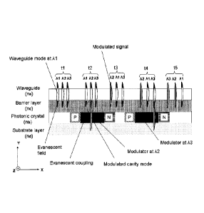
Figure 5 shows the principle of operation of the device. This is a schematic
representation of a multiwavelength signal propagating along the waveguide at
different times. In this case, the device has two resonators resonant at
22,23.
CA 02843546 2014-01-29
WO 2013/017814 PCT/GB2012/000618
7
At time t1, a multiwavelength signal represented by three waves with
wavelength
21,22,23 is coupled to the waveguide. The waveguide carries a single mode
defined
by a mode propagation vector k = 27rneff I 20 where Ao is the vacuum
wavelength and
neff is the effective refractive index of the waveguide at that wavelength.
The signal
travels in the waveguide via total internal reflection generating an
evanescent field
extending in the barrier layer.
At time t2 the multiwavelength signal passes over a first defect-cavity
resonator. The
evanescent tail of the mode propagating through the cavity extends into the
barrier
layer resulting in the evanescent coupling between the waveguide mode and the
cavity
mode. The first defect-cavity resonator is designed to be resonant at A2,
leading to the
spontaneous coupling of the A2 component of the signal to the defect-cavity
resonator.
Signal modulation is achieved by applying a voltage across the PIN junction.
This
generates a current across the defect-cavity modifying the refractive index
and the
resonant wavelength of the cavity via the carrier-plasma dispersion effect.
When the
cavity is off resonance, the A2 component passes over the cavity without being
affected. Hence, by varying the voltage applied to the PIN junction, the A2
light can be
selectively modulated. Figure 6 shows experimental data on this.
Alternatively,
modulation may be achieved by using a defect-cavity resonator formed in a
Silicon/Germanium multilayer 23 embedded in a biased PIN junction. Generation
of a
field across the PIN junction shifts the absorption band of the
Silicon/Germanium
multilayer. By varying the field across the PIN junction, the resonator can be
operated
as an electroabsorption modulator.
At time t4 the multiwavelength signal passes over the second defect-cavity
resonator
with resonant wavelength A3, leading to the coupling and modulation of the A3
component of the signal. At time t5 the modulated mode at A3 couples back to
waveguide. Hence, the light at the output of the waveguide is wavelength
division
multiplexed, with different wavelengths modulated to carry different
data/information.
Whilst two resonators are shown, it will be appreciated that the basic
principle of
operation shown in Figure 5 can be extended to N defect-cavity resonators with
the
primary limitation being the free spectral range of the resonator. In many
cases, single
CA 02843546 2014-01-29
WO 2013/017814 PCT/GB2012/000618
8
mode photonic crystal cavities may be used giving a free spectral range in
excess of
500nm, thereby providing a very large number of WDM channels.
The coupling strength between the waveguide and the cavity modes is determined
by
the spatial mode overlap and the wave-vector matching between the two modes.
Spatial overlap is controlled by the thickness of the barrier layer and the
design of the
defect-cavity resonator. The evanescent coupling between the waveguide and
cavity
modes occurs in the barrier layer. As a result, the thickness of the barrier
layer controls
the degree of overlap between the evanescent tails of the two modes [Optics
Letters
30, 1476-1478 (2005)1.
Figure 7(a) shows the mode profile of an example resonator. The defect-cavity
resonators are designed to have a mode volume of up to ten cubic resonant
wavelengths. As a result of this strong spatial confinement, the supported
mode has a
broad wave-vector space (broad momentum distribution), see Figure 7b. To
achieve
coupling between the cavity mode and bus waveguide, there must be a k-space
overlap between the two (see Figure 7c for the corresponding wave-vector
space).
Figure 8a shows a close-up of the overlap area of the wave-vector space of the
cavity
with the wave-vectors of two different waveguides marked (A and B). With an
appropriate choice of bus waveguide effective refractive index, there is a
strong overlap
resulting in strong coupling into the cavity, see curve A. Curve B shows that,
due to the
complexity of the k-space profile displayed in Figure 8a, a relatively small
change in neff
of the bus waveguide can change the overlap dramatically, therefore reducing
the
coupling efficiency. Current fabrication technologies can control the neff of
the bus
waveguide within the necessary tolerances. Figure 9 shows an experimental
demonstration of this point. In this case, the cavity exhibits two modes with
different
resonant frequencies and wave-vector distributions. By changing the waveguide
neff the
coupling into both modes can be widely varied.
Figures 10-12 show an example of the way a photonic crystal cavity can be
engineered
so that the cavity mode exhibits a wave-vector space suitable for matching to
that of a
specific waveguide.
CA 02843546 2014-01-29
WO 2013/017814 PCT/GB2012/000618
9
Figure 10 shows a standard PhC lattice with inter-hole spacing along the x-
direction xh
and inter-hole spacing in y-direction yh. By distorting/squeezing/stretching
the normal
(hexagonal) photonic crystal lattice, the wave-vector space can be made to
develop
higher intensities in the desired regions, giving improved coupling.
Using a hexagonal lattice with an inter-hole spacing (spacing between the next
neighbouring holes) equal to the lattice period a as a starting point, the
lattice can be
distorted by stretching/squeezing the lattice in the x-direction and/or by
stretching/squeezing the lattice in the y-direction. In the x-direction, the
inter-hole
distance xt, changes from its original value a to a higher or smaller value
and/or
according to a analytical formulation. Likewise, in the y-direction, the
vertical inter-hole
spacing yh changes from its original value (sqrt(3)/2)*a to a higher or
smaller value
andlor according to a analytical formulation. As a result, the mode
distribution is either
indirectly altered due to changes in the photonic-crystal band-structure and
their
penetration depths in different directions; and/or directly altered due to
mode-
interaction with certain holes. This allows coupling to different types of
photonic crystal
cavities giving improved flexibility in the choice of parameters such as free
spectral
range and Q-factor.
The coupling efficiency of a specific photonic crystal cavity can be
tuned/adjusted
without influencing the cavity design strongly or even switching to a
different type of
cavity. An alternative approach to engineering the cavity k-space is to
introduce a slot
into the cavity, similar to that employed in [Applied Physics Letters 94,
063503 (2009)
the contents of which are incorporated herein by reference] and/or rotating
the cavity
with respect to the waveguide.
Figure 11 shows the wave-vector space intensity profile. By reducing this
inter-hole
spacing, distorting the original hexagonal lattice, the intensity of the wave-
vector space
increases in the circled region. In addition to the specific increase of
intensities within a
desired k-space region the lattice distortion can also be used to obtain the
opposite
effect. In that case, the intensities around k = 0 (region of inhibited total
internal
reflection) can be reduced in order to decrease the photon loss out of the
cavity. By
either stretching/squeezing the lattice in x- and/or y-direction the Quality
factor of a
cavity can be improved.
CA 02843546 2014-01-29
WO 2013/017814 PCT/GB2012/000618
Figure 12 shows the measured extinction ratios of the fundamental mode of a
PhC
cavity, as a percentage function of change in yh.. It can be observed that the
extinction
ratio decreases with an increase in Yh percentage.
5 Relative to previous works, such as US 6411752 and Optics Letters 30,
1476-1478
(2005), in the device of the present invention, the options for wave-vector
matching are
greatly improved and efficient coupling between two dissimilar modes becomes
possible. This principle of k-space matching allows the creation of a range of
devices
for many different applications. The following equation shows how this may be
10 optimised for a particular application:
1 1 1
Q001 Qdesign aoupling Q fabrication
Qdesign is the 0-factor of the cavity in isolation, given by simulation,
0c.oupting depends on
the real space and k-space overlap between the bus waveguide and cavity mode.
()fabrication is given by the fabrication processes used to create the device.
The transmission (of the bus waveguide) on resonance with a resonator is given
by:
2 2
T¨ total _t_ total
2 2
Qdesign >fabricasion
For typical values of 0
¨clesign=500,000,
¨fabncation=750,000, 0 10,000, the resonant
¨total= -
transmission can be as low as 0.1%. Considering that the coupling losses of
light
between a lensed optical fiber and a SiONx waveguide can be as low as 0.2dB,
this
system allows the creation of an optical modulator with high extinction ratios
and low
insertion losses. The modulation speed can be very high (greater than 40GHz)
as the
Q is sufficient to allow carrier depletion to be used. For 0tota1=100,000, T
can be as low
as 6%, meaning that 94% of the light is coupled into the cavity making this
configuration very promising for non-linear applications.
CA 02843546 2014-01-29
WO 2013/017814
PCT/GB2012/000618
11
A number of materials may be used for the construction of the WDM modulator
device
6. The waveguide may be of a polymer such as Silicon oxynitride or of more
complex
composite structures such as TriPleXThl or HYDEXR, The barrier layer may be a
dielectric material such as silica, deposited chemical vapour deposition
techniques or
using spin-on glass. The photonic crystal slab may be manufactured in Silicon,
Silicon
Nitride or in a III-V semiconductor material such as Indium Phosphide, Gallium
Arsenide, Indium Gallium Phosphide or Gallium Nitride. It could also be made
of a
Silicon/Germanium multilayer. The structure of the photonic crystal lattice
may vary
according to specifications as well as the number and design of defect-cavity
resonators and resonator¨modulators. The lower cladding is typically made of
silica,
though air is possible in some instances. The substrate is silicon or a III-V
semiconductor.
In addition, a number of optional functions may be incorporated into the
device. For
example, each resonator in the WDM device can perform a different signal
processing
function, including that of filter, ON/OFF switch, amplitude modulator and
dispersion
compensator.
A plurality of resonators can be coupled together to form a coupled cavity
waveguide
also referred to as coupled resonator optical waveguide (CROW). In this
configuration
the waveguide operates as an optical delay line with each defect-cavity
producing a
delay, thus producing a "slow light" overall. This design can be used to
achieve a "flat-
top" response function by combining a near-unity transmission for a given
wavelength
range (typically 0.1-10 nm) with a very sharp cut-off. Such response functions
are
particularly well suited for data transfer application.
A different type of resonator with engineered dispersion, referred to as
"white light"
cavity, has an optical path that is held constant over a given wavelength
interval. In
order to achieve the white light cavity condition ( n =
cst ), the refractive index of the
cavity has to increase with wavelength. This requires operation in the "fast
light" regime
where the group velocity acotak-4Ø Such "anomalous" dispersion
characteristics
can be achieved by dispersion engineering over a narrow wavelength range (e.g.
AX=e1nm, Arr-,100 GHz). This may be implemented by adding a cavity into the
mirror
regions of the the resonator, so that it acts as a Gires-Tournois
Interferometer or by
CA 02843546 2014-01-29
WO 2013/017814 PCT/GB2012/000618
12
altering the waveguide portion of the resonator by means similar to those
described in
Optics Express 16, 6227-6232 (2008).
Figure 13 shows a transmission spectrum calculated across a bandwidth of lOnm
for
(a) a conventional cavity and (b) a white light cavity. The solid and dashed
lines
represent the transmission curves corresponding to a cavity with a refractive
index of
3.50 and 3.52 respectively. In the conventional cavity case (a), tuning the
refractive
index by An=0.02 changes the cavity resonance curve by rz-,3 rim, according
to An/ n = .6.1/2 . When considering the white light cavity (b), tuning the
cavity by
An=0.02 turns the resonance entirely on and off (dashed line). This means that
any
switching action depends on the loss-limited quality factor "0" as in a), but
the
bandwidth that can be accommodated depends on the spectral range over which
suitable dispersion engineering can be achieved.
Other combinations of individual defect-cavity resonators can be chosen to
create
degenerate resonances at the resonance frequency. A cavity, or a combination
of two
cavities, can be designed such that it exhibits two degenerate resonances at
the
resonance frequency. This ensures that light coupled out of the cavity into
the bus
waveguide destructively interferes in the backward direction reducing or
eliminating
backward directions. A cavity exhibiting a single mode acts as a notch filter
and will
couple light back into the waveguide when on resonance. For some applications
(where an optical isolator is inserted between the source and modulator for
example),
this backreflection is not a problem, making the single cavity approach an
appropriate
solution.
A resonator-modulator may be configured as a frequency-selective
photodetector.
Figure 14 shows a cross sectional view of the WDM modulator device operating
as a
frequency selective photo-detector. In this case, the defect-cavity is doped
with an
impurity 32 such as hydrogen or silicon. The doped defect-cavity 36 has an
absorption
band capable of generating photo-excited charge carriers upon coupling of a
propagating mode at the resonant wavelength /10. The charge carriers are then
extracted by the biased PIN junction surrounding the doped defect-cavity,
giving rise to
a photocurrent. The photocurrent, measured with a current detector 34 is
proportional
to the amount of wavelength-specific photo-generated carriers.
CA 02843546 2014-01-29
WO 2013/017814 PCT/GB2012/000618
13
Although the invention has been described primarily with reference to photonic
crystal
cavity defect resonators, other resonators may be used. For example, each
resonators
may based on a metallic structure, such as a nanoantenna physical Review
Letters
101, 116805 (2008)1, or a piasmonic resonator [Optics Express 19, (6) 5268
(2011)] or
split rings [Optics Letter 31, 1259 (2006)). Similarly to the photonic crystal
cavity case,
tight mode confinement results in a broad k-space thereby allowing coupling
between
the bus and resonator. Figure 15 shows one configuration. A bus waveguide 40
passes
vertically over a metallic nanostructure 44 such that evanescent tails of the
modes
overlap. The metallic nanostructure 44 is positioned on a suitable substrate
46 and the
entire structure encased in a suitable cladding material 42.
A skilled person will appreciate that variations of the disclosed arrangements
are
possible without departing from the invention. Accordingly, the above
description of the
specific embodiment is made by way of example only and not .for the purposes
of
limitation. It will be clear to the skilled person that minor modifications
may be made
without significant changes to the operation described.